
 Open Access Article
 This Open Access Article is licensed under a Creative Commons Attribution-Non Commercial 3.0 Unported Licence
Combined nanoarchitectonics with self-assembly and electrosynthesis for flexible PTCDIs@PEDOT films with interpenetrating P–N heterojunctions†
Nan
Gao
a,
Zexu
Xue
b,
Jiarui
Yu
a,
Shuai
Chen
 *a and
Ling
Zang
*c
*a and
Ling
Zang
*c
aFlexible Electronics Innovation Institute and School of Pharmacy, Jiangxi Science & Technology Normal University, Nanchang, Jiangxi 330013, China. E-mail: shuaichen@jxstnu.edu.cn; Fax: +86-791-88537029; Tel: +86-791-88537029
bSchool of Physics and Technology, Wuhan University, Wuhan, Hubei 430072, China
cNano Institute of Utah and Department of Materials Science and Engineering, University of Utah, Salt Lake City, Utah 84112, USA. E-mail: lzang@eng.utah.edu; Fax: +1-801-581-4816; Tel: +1-801-587-1551
First published on 2nd December 2021
Abstract
A novel synthesis method for fabricating large area, uniform bulk-heterojunction films with electron donor and acceptor materials homogeneously distributed among each other forming a bicontinuous network morphology is reported. The acceptor part was fabricated as nanofibers self-assembled from perylene tetracarboxylic diimide (PTCDI) molecules, which form a typical n-type semiconductor. The donor part was a classic P-type conducting polymer, poly(3,4-ethylenedioxythiophene) (PEDOT), which can be electrochemically polymerized from the EDOT monomer directly inside the nanofiber mesh, forming an interpenetrating P–N network. The nanofiber-based P–N heterojunction film demonstrates significant photocurrent generation. The facile and universal fabrication process combining in situ electrochemical polymerization with molecular self-assembly may find broader application in materials fabrication and structural engineering for P–N heterojunctions in photovoltaics and other optoelectronics.
1 Introduction
The P–N junction plays a key role in most semiconductor electronic and optoelectronic devices, such as transistors, diodes, solar cells, sensors and so on.1,2 For an organic semiconductor (mostly π-conjugated molecules), the P–N junction is normally composed of an electron donor (P-type) interfaced with an acceptor (n-type). Taking advantage of the vast options in molecular design and structural engineering, the organic P–N junction can potentially be constructed with an optimal energy level offset, maximal interfacial contact and continuous charge transport pathways, thus affording highly efficient photoinduced charge separation.2 Moreover, organic semiconductors are also superior to inorganic counterparts regarding low-cost fabrication, ease of large area processing, and compatible flexible and light weight plastic substrates. Combination of these unique features has made organic semiconductors and devices attract an increasingly enormous amount of research interest and effort in the past decades for future application in electronics and optoelectronics, particularly in flexible, wearable formats.3In the last few decades, organic P–N bulk heterojunctions (BHJs) have been fabricated from conducting polymers (CPs; e.g., P3HT) and fullerenes (C60) and employed in film photovoltaics, which can be developed into print manufacturing of solar cells.4 Similar BHJ structures also have been developed for small molecules that function as electron donors and acceptors.3 Ideally, these BHJ structures can be formed via simple solution processing, either through self-assembly in the solution phase or on a surface during solvent evaporation. One technical challenge of solution processing lies in the control of phase segregation of the P or the N part.5,6 For example, in the case of P3HT/C60, C60 tends to aggregate to form large crystals, and such phase segregation leads to a decrease in the P–N interfacial contact, and thus lowers photoconversion efficiency.7 Therefore, it is imperative to develop some unique ways to control the structure and morphology of P–N interfaces, to approach nanoscale interpenetration of P and N phases to reach the maximal contact for charge separation. Meanwhile, the interpenetrating network thus formed helps stabilize the BHJ morphology by spatially retraining the molecular diffusion and phase growth of the P and N parts.
As a classical and well-known organic n-type semiconductor molecule, perylene tetracarboxylic diimide (PTCDI) molecules consist of a stiff, planar, aromatic and fused-ring perylene skeleton and side-chain modifications at the imide- or bay-positions.8,9 They are widely used as visible-light absorbers or non-fullerene acceptors in photocatalysis, sensors, organic field effect transistors (OFETs), organic light-emitting diodes (OLEDs), dye-sensitized or BHJ organic photovoltaics (OPVs), etc.10,11 These molecules have a large π-conjugated area, allowing effective overlap of the frontier molecular orbitals of neighboring molecules, resulting in good electron transport performance. While PTCDIs have been employed in various molecular photovoltaics fabricated by solution processing,4 there remains a challenge of how the phase segregation of PTCDI that tends to aggregate to form large crystals due to the strong π–π stacking interaction between the molecules can be minimized. One way to inhibit the molecular aggregation of PTCDIs is to change the molecular structure by modifying the bay area with bulky, steric side groups that may reduce the cofacial stacking and aggregation.11,12 However, the weakened intermolecular stacking may also result in decreased charge transport that is normally mediated by π–π electronic coupling.
To address such a tradeoff, fabrication of the PTCDI phase (here specifically in the form of nanofibers) in a separate step, bisolvent interfacial self-assembly, allows us to control the size and morphology by optimizing the self-assembly conditions (solvents, concentration, etc.).9 1D nanostructures can be easily formed through π–π molecular interactions between neighboring PTCDIs molecules via interfacial phase transfer in the bulk solution system developed by our group.9 The elongated fibril structure of PTCDI is conducive to the long range electron transport (intermolecular charge delocalization) mediated by the cofacial π–π stacking between the molecules along the long axis of nanofibers.13,14 Photoinduced electron transfer and charge separation between PTCDI nanofiber and surface coated P3HT and other donor molecules have previously been observed in our lab.9,13,15 Moreover, PTCDIs materials are extremely robust regarding both thermal- and photo-stability, and these materials have strong absorption in the visible region.16 With the small size (thus large surface area) and interconnected network of the nanofibers, it is feasible to construct homogeneous BHJs with maximal P–N contact while still maintaining a continuous charge transport path through nanofibers.
Herein, we report on a novel method to fabricate uniformly interpenetrating P–N heterojunctions in the form of an n-type nanofiber network filled with CPs. As shown in Fig. 1, the fabrication process is carried out in two steps: self-assembly of PTCDI molecules into nanofibers in a solution, followed by the deposition of the nanofibers onto an ITO electrode, through which the electrochemical polymerization will produce and grow a polymer phase filling in the network meshes of nanofibers. When deposited on a substrate, the nanofibers intertwine, forming a three dimensionally interconnected network, suited for blending with the polymer grown therein. PTCDIs form a typical n-type material, and two PTCDI molecules (with different side groups, R as shown in Fig. 1) with good solution solubility and molecular assembly capability were selected.8,9 Electrochemical polymerization, as a user-friendly and precisely controlled technique to construct CP films on stiff or flexible electrodes, was employed in this study to prepare the polymer film on the electrode. The polymerization was performed on the 3,4-ethylenedioxythiophene (EDOT) monomer, which is a thiophene ring modified with an ethylene oxide group.17 The polymer thus generated, PEDOT, represents one of the most commonly used P-type polymers in solar cells, photo-/electro-catalysts, solid-state capacitors, transparent electrodes, functional coatings and many other electronic and optoelectronic devices.18 In contrast to other CPs, PEDOT has advantages such as excellent thermal and chemical stability, tunable redox behavior, good hole conducting features, broad absorption overlaps with the solar spectrum, etc.18–20 In this regard, the work reported herein would provide an alternative pathway to understand and improve the application of PTCDIs and PEDOTs in optoelectronics, especially concerning the nanoscale engineering and optimization of P–N BHJ with the aim to enhance the photoinduced charge separation.
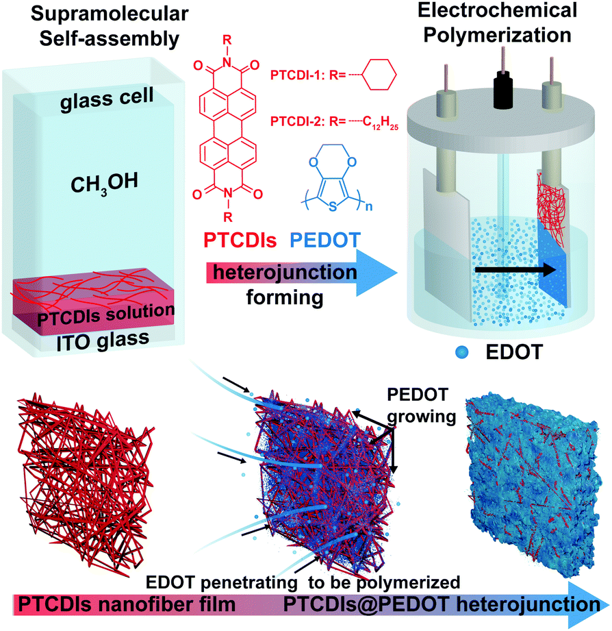 | ||
| Fig. 1 Schematic illustration of the fabrication process for PTCDIs@PEDOT nanofiber heterojunction film via a two-step process. | ||
2 Results and discussion
As illustrated in Fig. 1, the self-assembly was performed via a phase transfer process between a “good” and a “poor” solvent, where the slow mixing of two solvents provides an ideal medium for optimizing the molecular assembly to form a high crystalline phase of a well-defined shape and size as is widely practiced by us and others.9,14 Moreover, the bisolvent method allows in situ deposition of the nanofibers formed thereof onto a ITO glass plate placed at the bottom of the container (Fig. 1), as recently evidenced in our lab.21 Different from the common post-assembly transferring methods,22,23 the in situ deposition helps maintain the original morphology of nanofiber interconnection and the porosity thus formed. The solvent assisted relaxation of nanofibers onto the ITO substrate also enforces maximal interfacial contact that is conducive to the electrochemical polymerization to be performed later.Trichloromethane (CHCl3) or methylene chloride (CH2Cl2) was chosen as the “good” solvent, and methanol (CH3OH) as the “poor” solvent, which is lighter and can be poured in slowly atop the good solvent with dissolved PTCDI molecules. The volume ratio of poor to good solvent was set at 10![[thin space (1/6-em)]](https://www.rsc.org/images/entities/char_2009.gif) :1. For the two PTCDIs, the self-assembly was investigated in both CH2Cl2 and CHCl3 solvents. Due to different matching relations between PTCDI molecular structures and bisolvent systems,9,14 we found that only the solution of PTCDI-1 in CH2Cl2 and PTCDI-2 in CHCl3 could produce uniform nanofibers, and the overall network architecture and porosity are quite homogeneous throughout the whole film as deposited on ITO, as revealed by both the optical microscope (Fig. S1, ESI†) and SEM imaging (Fig. 2a and b). The two PTCDI nanofiber films thus fabricated were used as the working electrodes for electrochemical polymerization of the EDOT monomer, following the common protocols as previously established regarding electrolyte, concentration, electrode potential control, etc.24 The extent of polymerization was controlled and quantified by polymerization charge (in units of mC) rather than polymerization time, with the aim to provide common ground for comparison between the different PTCDI nanofibers, for which the different conductivity, porosity or contact with ITO may lead to different polymerization efficiencies.
:1. For the two PTCDIs, the self-assembly was investigated in both CH2Cl2 and CHCl3 solvents. Due to different matching relations between PTCDI molecular structures and bisolvent systems,9,14 we found that only the solution of PTCDI-1 in CH2Cl2 and PTCDI-2 in CHCl3 could produce uniform nanofibers, and the overall network architecture and porosity are quite homogeneous throughout the whole film as deposited on ITO, as revealed by both the optical microscope (Fig. S1, ESI†) and SEM imaging (Fig. 2a and b). The two PTCDI nanofiber films thus fabricated were used as the working electrodes for electrochemical polymerization of the EDOT monomer, following the common protocols as previously established regarding electrolyte, concentration, electrode potential control, etc.24 The extent of polymerization was controlled and quantified by polymerization charge (in units of mC) rather than polymerization time, with the aim to provide common ground for comparison between the different PTCDI nanofibers, for which the different conductivity, porosity or contact with ITO may lead to different polymerization efficiencies.
 | ||
| Fig. 2 (a–d) SEM images of (a) PTCDI-1 nanofiber film, (b) PTCDI-2 nanofiber film, (c) PTCDI-1@PEDOT and (d) PTCDI-2@PEDOT films. PEDOT in both films was polymerized at 30 mC. (e–g) Elemental mapping of the PTCDI-2@PEDOT film for (e) nitrogen, (f) sulfur and (g) combination of the two elements. | ||
Fig. 2c and d show the SEM images of PTCDI-1@PEDOT and PTCDI-2@PEDOT, respectively, both with PEDOT formed inside the nanofiber network through in situ electrochemical polymerization. It is clearly seen that PEDOT is homogeneously coated onto PTCDI nanofibers throughout the film, no matter where the nanofibers are located, either deep inside close to the ITO surface or far on the top of the film. Such homogeneous polymerization and surface coating is likely due to the high electrical conductivity of the PTCDI nanofibers (enabled by the π–π stacking as pointed out above) that makes the whole nanofiber film part of the working electrode function for polymerization. The elemental mapping (analysis) of a film of PTCDI-2@PEDOT (Fig. 2e–g) further confirms the homogeneous distribution of PEDOT across the nanofiber network, wherein the sulfur element (marked in blue) intrinsic to the PEDOT chain is distributed uniformly across the nanofiber matrix (PTCDI, nitrogen element marked in red). Meanwhile, the formation of the PTCDIs@PEDOT nanofiber composite was also confirmed by AFM imaging (Fig. S2, ESI†). Compared with smooth PTCDI nanofibers, the PTCDIs@PEDOT composite film demonstrates much rougher surface that is consistent with the surface of a pure PEDOT film regarding surface morphology and roughness. Upon washing with CH2Cl2, the PTCDI-1@PEDOT composite film (polymerized at 100 mC) still retained the same morphology with the shape-defined PTCDI nanofibers to be persistent as their initial state (Fig. S3, ESI†). This indicates the complete coverage of PTCDI nanofibers with PEDOT. Since PEDOT is insoluble in CH2Cl2, PEDOT coating on the top and bottom surfaces of PTCDI nanofibers films can protect them from being dissolved by CH2Cl2 (a good solvent for PTCDI molecules).
The homogeneous polymerization also benefits from the effective diffusion of the EDOT monomer into the nanofiber network, wherein the hydrophobic character of PTCDI is conducive to draw EDOT from the relatively hydrophilic and polar solvent of ACN (which was used in this study as the electrolyte solvent). The polymerization of EDOT starts to occur on ITO under an applied voltage of 1.3 V. As the polymerization continues with increasing polymerization charge, PEDOT keeps growing along the ITO surface and PTCDI nanofibers throughout the film network, and eventually fills the entire nanofiber mesh as shown in Fig. 3a. After the nanofiber mesh is filled up, continuous polymerization forms extra PEDOT in a morphology of distinct clusters over the film surface as is clearly seen from the SEM images (Fig. S4, ESI†). A PTCDI nanofiber film completely filled with PEDOT can be peeled off from the ITO surface to act as a free-standing film as shown in Fig. 3b. The mechanical strength is largely due to the interconnected network of PTCDI nanofibers that is now reinforced by the filling of PEDOT.
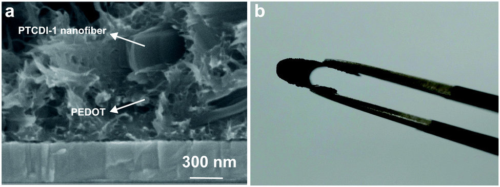 | ||
| Fig. 3 (a) Cross-sectional SEM image and (b) the photo of free-standing and flexible PTCDI-1@PEDOT (600 mC) film. | ||
Solutions of PTCDIs in CHCl3 (5 μmol L−1) demonstrate similar absorption spectra as presented in Fig. 4a and Fig. S5 (ESI†), with three characteristic peaks located around at 460, 490, and 528 nm corresponding to the 0 → 2, 0 → 1, and 0 → 0 π–π* electronic transitions.21,25 By contrast, self-assembled PTCDI nanofibers exhibit dramatic change in the absorption spectra, with the 0 → 1 and 0 → 2 absorption relatively increased and a new absorption band around 565 nm emerges, which is characteristic of the π–π stacking arrangement of the molecules.9,14 In comparison, a film of PEDOT fabricated on ITO via electrochemical polymerization from EDOT under 30 mC of polymerization charge shows a broad absorption band covering most of the visible region and across near-infrared region (Fig. 4a), which is consistent with the blue color of the film. A composite of PTCDI and PEDOT would cover the whole visible and near-infrared region regarding light absorption that is essential for OPVs and other optoelectronic applications.
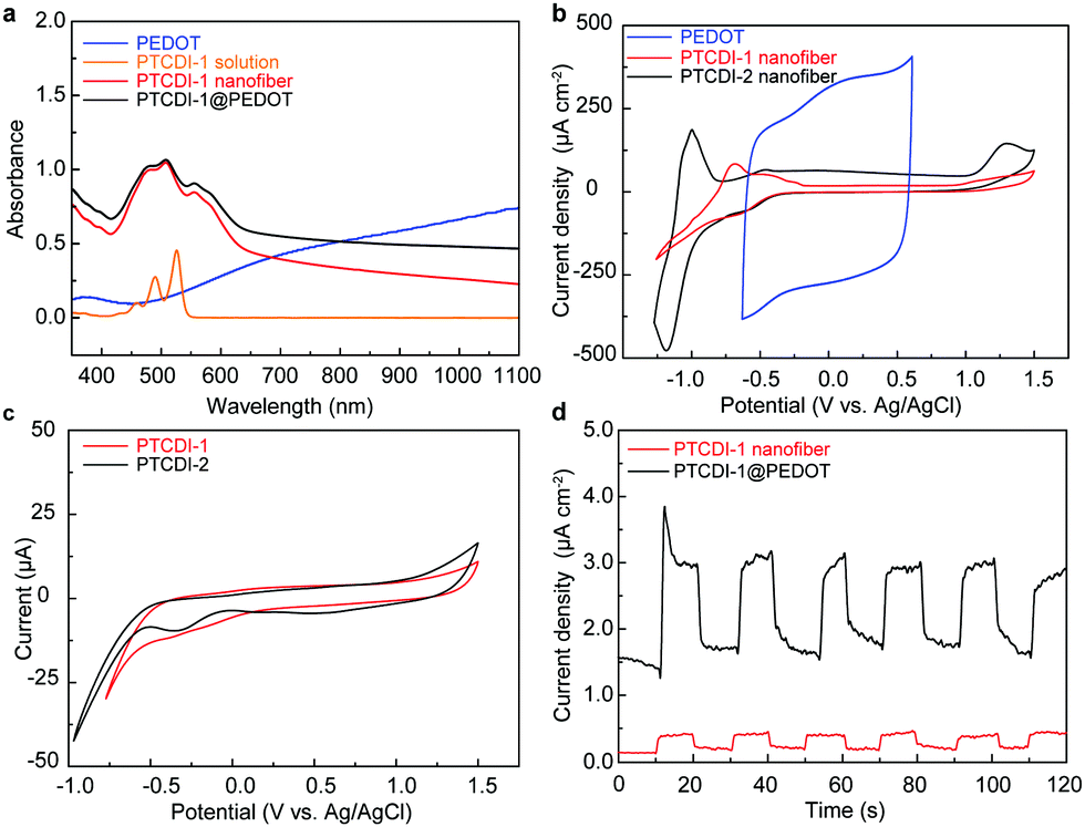 | ||
| Fig. 4 UV-vis spectra of (a) PEDOT film (synthesized under polymerization charge of 30 mC), 5 μM CHCl3 solution of PTCDI-1, film of PTCDI-1 nanofibers deposited on ITO glass, and film of PTCDI-1@PEDOT (30 mC); cyclic voltammograms of (b) films of PEDOT (30 mC), PTCDI-1 and PTCDI-2 nanofibers in H2O/LiClO4 (0.1 M) and (c) the PTCDI molecules in CHCl3/Bu4NPF6 (0.1 M). (d) Photocurrent measured for PTCDI-1@PEDOT composite in comparison to pure PTCDI nanofibers under white light irradiation (300 mW·cm−2). | ||
The electrochemical behavior of PTCDI molecules and as-prepared nanofiber films was studied in a three-electrode system in CHCl3 and aqueous electrolyte solution, respectively. As shown in the cyclic voltammograms (Fig. 4b), both the PTCDI nanofibers display a reduction process due to the one-electron reduction of the PTCDI component, which is consistent with that of PTCDI molecules dissolved in CHCl3 (Fig. 4c). Moreover, the nanofiber films exhibit a strong peak current relative to their molecules in solution, which can be explained by the effective electron delocalization mediated by the well-ordered stacking arrangement of PTCDIs, implying the promising potential of using PTCDI to build BHJs with PEDOT.
The PTCDIs@PEDOT nanofiber composite was also characterized for photocurrent generation, which is directly relevant to the P–N junction formed as well as the potential application in OPVs and other optoelectronics.13 As shown in Fig. 4d, significant photocurrent was obtained for PTCDI-1@PEDOT, whereas much less photocurrent was observed for the pure PTCDI nanofibers under the same experimental conditions. The increased photocurrent achieved was apparently due to the efficient photoinduced electron transfer from PEDOT to PTCDI, which in turn can be facilitated by the large area interfacial contact intrinsic to the BHJ structure of PTCDI-1@PEDOT as illustrated in Fig. 1. Significant photocurrent generation was also observed for PTCDI-2@PEDOT nanofiber composite as shown in Fig. S6 (ESI†). Compared to PTCDI-1@PEDOT, PTCDI-2@PEDOT has a relatively slow photocurrent response. This is likely due to the different morphology of the nanofiber films formed from the two PTCDIs. As shown in Fig. 2a and b, the nanofibers of PTCDI-1 and PTCDI-2 are approximately the same size, but have dramatically different morphologies when deposited on a substrate. The film of PTCDI-1 nanofibers possesses more open and better-connected porosity that is conducive to the formation of P–N junctions having maximal contact with PEDOT, whereas the film of PTCDI-2 nanofibers shows more tight intertwining and less open porosity, which limits the P–N contact with PEDOT. In general, the larger the P–N contact, the more efficient the photocurrent generation will be.26
The growth process of the PTCDI@PEDOT composite can also be verified by the UV-vis absorption and fluorescence microscopy images. As shown in Fig. 4a and Fig. S5 (ESI†), the absorption spectrum of a composite film exhibits not only the characteristic peaks of PTCDI in the range of 400–600 nm, but also increased absorption due to PEDOT in the longer wavelength up to near-infrared region. With increase of polymerization charge from 100 to 500 mC, the characteristic absorption peaks of PTCDI gradually disappear (Fig. 5), indicating increasing amount of PEDOT formed and coated on PTCDI nanofiber surface, which would eventually make the composite become dominated by the PEDOT in light absorption. The same polymerization growing process was also monitored by fluorescence imaging as shown in Fig. S7 (ESI†). Clearly, as the polymerization increases, the red luminescence of PTCDI nanofibers becomes more dimmed and eventually disappears. This can be attributed to the photoinduced electron transfer from PEDOT to PTCDI or the competitive light absorption from the increasing coating of PEDOT, both of which result in fluorescence quenching of PTCDI.
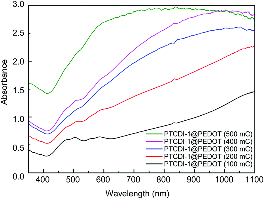 | ||
| Fig. 5 UV-vis absorption spectrum of PTCDI-1@PEDOT with different polymerization charge. | ||
Since PTCDIs and PEDOT have great superiority in their respective fields but quite different optoelectronic features, the optical, electrical and electrochemical performances of this type of heterojunction can be tuned as required to meet special uses. While considering the presence of their many derivatives as well as the large number of other compounds in their respective fields, many matching interfaces and highly efficient heterojunctions can be expected. In particular, this approach could bring novel chance for those semiconductors with relatively poor molecular electron-activity and aggregated state is required for use. That is, it will promote the development of the supramolecular field itself. On the other hand, we believe the employing 1D nanofiber structures of P-type conducting polymers as network electrodes will give much more chance to develop N–P or P–N type heterojunctions to break through their current application problems in current fields. Nevertheless, the internal interface and energy band match of P–N heterojunctions including PTCDIs and PEDOT here, and that between them and external electrodes, electrolytes, active chemicals or other interfaces surrounding them still meet many challenges, requiring thefuture cooperation of researchers in material, electronic, physical, nanotechnological, mechanical processing and other fields. Furthermore, the rapid development of flexible electronics demands more about heterojunction devices. The intrinsic flexibility of an all-organic heterojunction architecture like optimal PTCDI@PEDOT here may bring great opportunity in these fields.
3 Conclusions
In summary, we put forward a two-step process for the fabrication of an all-organic optoelectronic film with a contiguous interpenetrating P–N heterojunction network structure, by combining 1D supramolecular self-assembly of PTCDIs and electrochemical growth of PEDOT. The N part in the form of 1D “crystalline” nanofibers utilizes molecular mass transfer between good and poor solvents, π–π stacking growth and simple solvent evaporation processes, which can eliminate the complex material interactions. Besides easy molecule structure design and synthesis, the nanofiber feature can be easily changed by selecting the solvent system and other environmental parameters. The P part on the basis of mild and highly controllable polymerization of electrically active monomer into CPs onto the n-type fiber electrode was easily carried out. Moreover, the interpenetrating degree and composite morphology can be obtained as required. Well-defined PTCDI nanofibers possess high-speed channels for electron transport and good porous framework for PEDOT growth and electrolyte ion migration, while PEDOT filling the nanofiber network offers continuous hole transport support and robust film morphology which can be controlled by the electrosynthesis process.4 Experimental
4.1 Materials
All organic solvents were purchased from J&K Scientific Ltd. 3,4,9,10-Perylenetetracarboxylic dianhydride (PTCDA), 3,4-ethylenedioxythiophene (EDOT), anhydrous zinc acetate, imidazole, cyclohexylamine and dodecylamine were purchased from TCI (Shanghai) Development Co., Ltd. Lithium perchlorate (LiClO4, 99%) was purchased from Shanghai Vita Chemicals Reagent Co., Ltd. All these reagents were of AR grade and were used without further purification. Tetrabutylammonium hexafluorophosphate (Bu4NPF6, 99%, Shanghai Vita Chemicals Reagent Co., Ltd) was dried under vacuum at 60 °C for 24 h before use. Details of the synthesis of PTCDI 1 and 2 are provided in the ESI† with the synthesis pathways shown in Scheme S1.4.2 Fabrication of PTCDI nanofiber electrodes
PTCDI nanofiber electrodes were prepared via the in situ interfacial self-assembly method. ITO glass (1 × 2 cm) was washed by CH2Cl2, acetone, distilled water, and ethanol, respectively, and then was placed at the bottom of a glass cell (2.1 cm × 1.1 cm × 6 cm) after 15 min ultraviolet-ozone treatment. The saturated solutions of PTCDIs (0.3 mL CHCl3/CH2Cl2, as “good” solvent) and “poor” solvent (3 mL, CH3OH) were successively injected in the glass cell. At this time, the formation of red aggregates at the bottom could be observed. The glass cell was left standing until no aggregate formed, and then the supernatant was carefully removed and the remaining liquid was left to evaporate. It was observed that red nanofibers were evenly covered on the ITO glass substrate, which was then washed with CH3OH and dried under vacuum at 60 °C.4.3 Fabrication of PEDOT and PTCDIs@PEDOT films
PEDOT and PTCDIs@PEDOT films were fabricated in a three-electrode system at room temperature via chronoamperometry at 1.3 V. ITO glass or PTCDIs nanofiber electrodes were used as working electrodes for preparation of PEDOT or PTCDIs@PEDOT, while Ag/AgCl was used as the reference electrode and the platinum plate (1.5 × 1.5 cm) as the counter electrode in acetonitrile (ACN)/Bu4NPF6 (0.1 M) electrolyte solution containing the EDOT monomer (5 mM). The amount of polymerization charge was measured by chronocoulometry. N2 was introduced into the electrolyte solution to expel oxygen for half an hour at room temperature prior to the polymerization of the monomer.4.4 Photocurrent measurements
A three-electrode system was used to test and compare the photochemical properties of the as-prepared films. An electrochemical workstation (Versa STAT 3, Princeton Applied Research) and a Xenon lamp (CEL-HXUV 300, Education Au-light Co., Ltd) were used as testing instruments. The working electrodes used in the test were PTCDIs nanofiber electrodes or PTCDIs@PEDOT electrodes with an effective area of 1 cm2, while Ag/AgCl was used as the reference electrode and platinum plate (1.5 × 1.5 cm) as the counter electrode in Na2SO4 electrolyte solution (0.1 M). The light source was incident from the back of the ITO glass. The light intensity (300 mW cm−2) was measured on an optical power meter (CEL-NP2000-2A, Education Au-light Co., Ltd).4.5 Characterization studies
UV-vis absorption spectra of PTCDIs in CHCl3, PTCDI nanofiber films, PEDOT film and PTCDIs@PEDOT films were collected using a UV-Vis spectrophotometer (Specord Plus 200 Analytik Jena, Germany). All as-prepared materials were characterized and confirmed using FT-IR spectral measurements (PerkinElmer Spectrum Two, Universal ATR Sampling Accessory), and the FT-IR spectra of PTCDI-1, PTCDI-2, PTCDI-1@PEDOT, PTCDI-2@PEDOT, and pure PEDOT are shown in Fig. S8 (ESI†). The polymerization of EDOT and electrochemical properties of materials were measured on a three-electrode system using an electrochemical workstation (Versa STAT 3, Princeton Applied Research). The morphology and microstructural observations were characterized via a metallographic microscope (LW300LJT, Beijing Cewei Optoelectronic Technology Co., Ltd), fluorescence microscope (OST-YW4000, Suzhou Oust Optical Instrument Co., Ltd), scanning electron microscope (SEM, FEI-QUANTA250, USA) and atomic force microscope (AFM, Bruker Dimension Icon, USA).Conflicts of interest
There are no conflicts to declare.Acknowledgements
We are grateful to the National Natural Science Foundation of China (No. 51863009 and 51763010).References
- A. Wadsworth, Z. Hamid, J. Kosco, N. Gasparini and I. McCulloch, Adv. Mater., 2020, 32, 2001763 CrossRef CAS PubMed.
- S. Chen, N. Gao, B. R. Bunes and L. Zang, J. Mater. Chem. C, 2019, 7, 13709–13735 RSC.
- J. Kim, D. Khim, J. S. Yeo, M. J. Kang, K. J. Baeg and D. Y. Kim, Adv. Opt. Mater., 2017, 5, 1700655 CrossRef.
- A. W. Hains, Z. Q. Liang, M. A. Woodhouse and B. A. Gregg, Chem. Rev., 2010, 110, 6689–6735 CrossRef CAS PubMed.
- K. K. Weng, L. L. Ye, L. Zhu, J. Q. Xu, J. J. Zhou, X. Feng, G. H. Lu, S. T. Tan, F. Liu and Y. M. Sun, Nat. Commun., 2020, 11, 2855 CrossRef CAS PubMed.
- J. W. Mok, Z. Q. Hu, C. X. Sun, I. Barth, R. Muñoz, J. Jackson, T. Terlier, K. G. Yager and R. Verduzco, Chem. Mater., 2018, 30, 8314–8321 CrossRef CAS.
- L. G. Li, D. L. Jacobs, Y. K. Che, H. L. Huang, B. R. Bunes, X. M. Yang and L. Zang, Org. Electron., 2013, 14, 1383–1390 CrossRef CAS.
- F. Würthner, Chem. Commun., 2004, 1564–1579 RSC.
- S. Chen, P. Slattum, C. Y. Wang and L. Zang, Chem. Rev., 2015, 115, 11967–11998 CrossRef CAS PubMed.
- M. Golshan, R.-T.-E. Ehsan, S.-K. Mehdi and R.-M. Hossein, Eur. Polym. J., 2020, 137, 109933 CrossRef CAS.
- Y. W. Duan, X. P. Xu, H. Yan, W. L. Wu, Z. J. Li and Q. Peng, Adv. Mater., 2017, 29, 1605115 CrossRef PubMed.
- P. Singh, A. Hirsch and S. Kumar, TrAC, Trends Anal. Chem., 2021, 138, 116237 CrossRef CAS.
- L. Zang, Acc. Chem. Res., 2015, 48, 2705–2714 CrossRef CAS PubMed.
- L. Zang, Y. K. Che and J. S. Moore, Acc. Chem. Res., 2008, 41, 196–1608 CrossRef PubMed.
- L. P. Yang, M. M. Wang, P. M. Slattum, B. R. Bunes, Y. H. Wang, C. Y. Wang and L. Zang, ACS Appl. Mater. Interfaces, 2018, 10, 19764–19772 CrossRef CAS PubMed.
- F. Würthner, C. R. Saha-Möller, B. Fimmel, S. Ogi, P. Leowanawat and D. Schmidt, Chem. Rev., 2016, 116, 962–1052 CrossRef PubMed.
- A. Elschner, S. Kirchmeyer, W. Lövenich, U. Merker and K. Reuter, PEDOT-principles and Applications of an Intrinsically Conductive Polymer, CRC Press, New York, 2011 Search PubMed.
- H. W. Chen and C. Li, Chin. J. Polym. Sci., 2020, 38, 435–448 CrossRef CAS.
- Q. Y. Fu, Y. D. Li, X. C. Wang, Q. Li, F. Wang and R. Q. Yang, J. Mater. Chem. C, 2020, 8, 17185–17193 RSC.
- H. Shi, C. C. Liu, Q. L. Jiang and J. K. Xu, Adv. Electron. Mater., 2015, 1, 1500017 CrossRef.
- Z. X. Xue, S. Chen, Y. Xue, O. A. Watson and L. Zang, Langmuir, 2019, 35, 12009–12016 CrossRef CAS PubMed.
- Y. K. Che, H. L. Huang, M. Xu, C. Y. Zhang, B. R. Bunes, X. M. Yang and L. Zang, J. Am. Chem. Soc., 2011, 133, 1087–1091 CrossRef CAS PubMed.
- M. Yanilmaz, M. Dirican, A. M. Asiri and X. W. Zhang, J. Energy Storage, 2019, 24, 100766 CrossRef.
- S. I. Cho and S. B. Lee, Acc. Chem. Res., 2008, 41, 699–707 CrossRef CAS PubMed.
- M. E. El-Khouly, A. El-Refaey, S. Y. Shaban and M. El-Kemary, J. Lumin., 2018, 196, 455–461 CrossRef CAS.
- H. Wu, H. G. Jile, Z. Chen, D. Xu, Z. Yi, X. Chen, J. Chen, W. T. Yao, P. H. Wu and Y. G. Yi, Micromachines, 2020, 11, 189 CrossRef PubMed.
Footnote |
| † Electronic supplementary information (ESI) available. See DOI: 10.1039/d1ma01015h |
| This journal is © The Royal Society of Chemistry 2022 |