
 Open Access Article
 This Open Access Article is licensed under a Creative Commons Attribution-Non Commercial 3.0 Unported Licence
Multicoated composites of nano silicon and graphene nanoplatelets as anodes in Li-ion batteries†
Pin-Yi
Zhao
 ab,
Antonio Ruiz
Gonzalez
ab,
Bing
Li
a,
Yuhan
Liu
bc,
Robert
Palgrave
b and
Kwang-Leong
Choy
*a
ab,
Antonio Ruiz
Gonzalez
ab,
Bing
Li
a,
Yuhan
Liu
bc,
Robert
Palgrave
b and
Kwang-Leong
Choy
*a
aInstitute for Materials Discovery, University College London, 120-124 Roberts Building, London, WC1E 7JE, UK. E-mail: k.choy@ucl.ac.uk
bDepartment of Chemistry, University College London, 20 Gordon Street, London, WC1H 0AJ, UK
cDepartment of Physics and Astronomy, University College London, Gower Street, London, WC1E 6BT, UK
First published on 10th March 2022
Abstract
A simple, non-vacuum aerosol-assisted chemical deposition (AACD) method was developed for the deposition of a homogeneous composite film of graphene nanoplatelets and nano silicon. The multicoated composite anode (with 10 wt% silicon) exhibited promising capacity retention of 85.8% after 500 discharge/charge cycles in Li-ion batteries.
The development of Li-ion batteries (LIBs) with high energy density and long cycle life is of significant importance in portable electronics, electric vehicles and energy storage for modern society needs.1–5 After decades of research, the typical carbon anode, graphite, is now reaching the theoretical capacity limit.6 As a promising alternative, silicon anodes are being intensively studied as the near-term solution.3 Silicon has: (1) a gravimetric specific capacity of 3579 mAh g−1
![[thin space (1/6-em)]](https://www.rsc.org/images/entities/char_2009.gif) 7–9 corresponding to Li15Si4 (space group I
7–9 corresponding to Li15Si4 (space group I![[4 with combining macron]](https://www.rsc.org/images/entities/char_0034_0304.gif) 3d), about ten times of graphite (372 mAh g−1); (2) low delithiation potential, ∼0.4 V vs. Li+/Li;10 (3) earth abundance (the second richest element in the Earth's crust) as well as low-cost and non-toxicity. However, the practical usage of silicon as the anode material is seriously crippled by two obstacles. The first obstacle is the huge volume expansion (270%),11 which further leads to severe pulverization of the anodes and rapid capacity fading, representing a formidable challenge for battery design.12 The second obstacle is the low electrical conductivity (1.56 × 10⁻³ S m−1),13 which leads to a delayed rate capability.14
3d), about ten times of graphite (372 mAh g−1); (2) low delithiation potential, ∼0.4 V vs. Li+/Li;10 (3) earth abundance (the second richest element in the Earth's crust) as well as low-cost and non-toxicity. However, the practical usage of silicon as the anode material is seriously crippled by two obstacles. The first obstacle is the huge volume expansion (270%),11 which further leads to severe pulverization of the anodes and rapid capacity fading, representing a formidable challenge for battery design.12 The second obstacle is the low electrical conductivity (1.56 × 10⁻³ S m−1),13 which leads to a delayed rate capability.14
To address the above two concerns and enhance the universal electrochemical performance of silicon anodes, one strategy is to design an anode based on silicon/carbon composites15 that could buffer the drastic volume variation and boost the electrical conductivity at the same time. Under a 2D conductive network, graphene16 has been incorporated into silicon anodes to accommodate the volume change and enhance the electrical and mechanical properties.17 Another strategy is the adoption of nano-sized silicon.18 Nano-silicon could alleviate mechanical breakdown, minimize total volumetric expansion, and deliver increased electron transport.19 Nano-silicon anodes of multiple configurations have been constructed.20 However, the costs of fabrication for these complex nanostructured anodes tend to be high and may encounter challenges in upscaling despite the outstanding performance.21
In this work, we develop non-vacuum aerosol-assisted chemical deposition (AACD) and apply it on LIBs. During the deposition process, a mixture of nano silicon was atomized to an aerosol and directed towards the mildly heated substrate, where the removal of solvent would lead to the composite being deposited directly. The deposition was repeated to lay down multicoated composite anodes. Compared with the traditional deposition process, the unique advantages of AACD22,23 include (1) simplified delivery through aerosol generation; (2) non-vacuum open atmosphere deposition; (3) lower deposition temperature, and thus energy-efficient;24–26 (4) multi-components formulated into a single mixture, thus enabling well-controlled stoichiometry; (5) ultrafine materials/fillers can be incorporated into the aerosol precursor, thus facilitating (nano)composite deposition.
Preliminary tests (experimental, ESI†) are illustrated through the dispersion test (Fig. S1, ESI†), contact angle (Fig. S2, ESI†), TGA (Fig. S3 and S4, ESI†), and electrochemical performance of the raw materials (Fig. S5, ESI†) with descriptions. The illustration of the AACD is displayed in Fig. 1a where an atomized aerosol was led towards the heated substrate. The substrate setting was tested using a thermographic image after the temperature reached equilibrium (inset in Fig. 1a). Using this method, the uniform thermal behavior of the substrate is validated, while the center has a higher temperature than the surroundings. The obtained spacer-based electrode is shown in Fig. 1b with a uniform appearance. Fig. 1c presents the adjusted coin-cell structure. Notably, as Li metal is arranged to the can cathode, the device would need to be tested counter-polarly, while the multicoated electrode is the cathode in a half-cell arrangement.
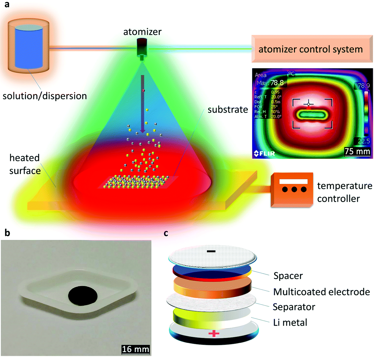 | ||
| Fig. 1 (a) Schematic of the AACD setup. Here, the dispersion/solution for the fabrication of the anode films is stored. The dispersion/solution is being atomized using airflow to generate a fine aerosol that is directed towards a heated substrate. The distribution of temperatures over the substrate (the inset photo) is shown using FLIR, (b) photo of the multicoated electrode after deposition by AACD using graphene nanoplatelets/silicon nanoparticle dispersion, and (c) schematic representation of the coin-cell structure where the multicoated electrode was fabricated via AACD. | ||
The powder X-ray diffraction patterns of the raw materials and the samples (sample description: Table S1, ESI†) are displayed in Fig. 2 with crystallographic planes and juxtaposition with the waterfall pattern to avoid overlapping. The graphene nanoplatelets display peaks at ∼26° and ∼55°.27 The diffractogram of the (00l) peaks are affected by the pressure and anisotropic platelet-like shapes of the graphene nanoplatelets.28 The series of peaks at 28.4° (111), 47.3° (220), 56.1° (311), 69.1° (400), and 76.4° (331) are indexed as crystallographic planes through the standard pattern of cubic silicon (JCPDS no. 27-1402).29 In the case of the composites, impurity peaks from SiC, SiO, or SiO2 are not detected. As the ratio of nano silicon increases, the corresponding peaks of the Si-nanoparticles become more prominent. The composition of the materials is further supported by the Raman spectra in Fig. S6 (ESI†) and X-ray photoelectron spectroscopy in Fig. S7 (ESI†).
 | ||
| Fig. 2 Powder X-ray diffraction of GNS5, GNS10, GNS20, and GNS30, overlapped and waterfall patterns. | ||
The discharge/charge curves are displayed in the cyclic type30 as shown in Fig. 3a–d (details in the presentation for cyclic discharge and charge pattern, ESI†). In addition, the specific charge capacity is shown in Fig. 3e–h, compared with their corresponding theoretical limits (dashed lines). It is shown that, as the concentration of nano silicon increases, the difference between the achieved specific capacity and the theoretical limit increases, indicating lower compatibility of the silicon nanoparticles with the graphene nanoplatelets. In other words, the room for improvement increases as the ratio of nano silicon increases, though the buffering of the volume expansion and the amount of nano silicon have to be balanced as is demonstrated in this work. While the graphene layer could promote electron transfer and keep the structural cohesion of the electrode, the competence of the graphene layer goes beyond the limit when too much volume expansion disturbs it. For the sample GNS10, the combined effect of nano silicon and graphene nanoplatelets reached the maximum. The sample delivers the optimal first specific charge capacity of ∼500 mAh g−1 with 72.2% capacity fulfilled (72.2% theoretical specific capacity shows up in the initial charge process). Compared with GNS10, GNS5 has a specific charge capacity of ∼425 mAh g−1, which is comparatively closer to the theoretical limit with 79.8% capacity fulfilled. Conversely, the capacity of GNS30 dropped rapidly from 200 mAh g−1 at the beginning to 60 mAh g−1 when 500 cycles ended. This drop could be attributed to drastic volume changes of nano silicon beyond the buffering of graphene nanoplatelets and consequent electrical detachment. The multicoated character of the as-processed samples is shown in the cross-sectional SEM images of Fig. 3. The nano silicon is well incorporated with graphene nanoplatelets to form the composite layers. Between the layers (apparent layer thickness: ∼0.2 μm) are visible voids where volume expansion could be buffered. The graphene structure would restrict the agglomeration of nano silicon by ordering their locations31 and reduce contact with electrolytes by covering the silicon nanoparticles with thin layers. It is noted that, however, the agglomeration increases with a higher concentration of nano silicon, being the most evident in GNS30. In this scenario, graphene nanoplatelets might have agglomerated.
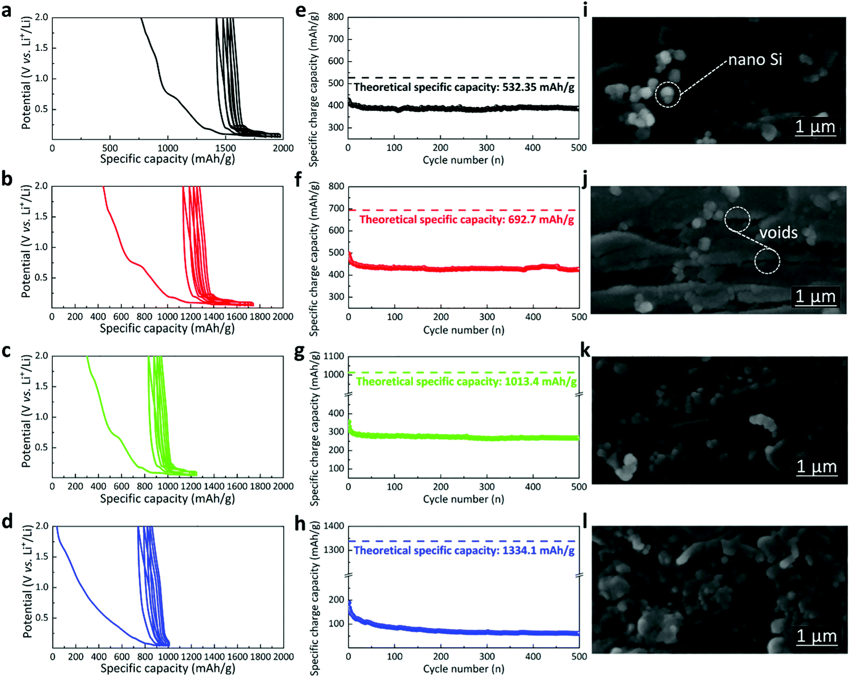 | ||
| Fig. 3 First five discharge/charge curves (cyclic type) at 0.17 A g−1 (a–d), specific charge capacity with calculated theoretical limits (e–h), and cross-sectional SEM images (i–l) of GNS5 (a, e and i), GNS10 (b, f and j), GNS20 (c, g and k) and GNS30 (d, h and l). | ||
Fig. S8 (ESI†) shows the cyclic voltammetry curves of the samples, intended to study the redox of the electrode materials. The discharge/charge patterns of GNS10 are plotted in Fig. 4a. It is evidenced that the curves exhibited a steady pattern with capacity slowly declining from 495 mAh g−1 to 425 mAh g−1 and capacity retention of 85.8%. The capacity retention is displayed in the histograms in Fig. 4b. It is shown that when 500 cycles finish, GNS5 and GNS10 have similar capacity retention (90.9% and 85.8%, respectively), while GNS20 and GNS30 are less stable (75.4% and 32.3%). GNS5 achieves 80.1% of the corresponding theoretical limit whereas GNS10 reaches 71.5%. On the contrary, GNS20 and GNS30 only get less than 40% of the corresponding theoretical limit fulfilled. There are four conceivable explanations for this: (1) clustering of nano silicon; (2) the rates of volume change diverging between nano silicon and graphene nanoplatelets,32 which could exacerbate the nano silicon exfoliation from the bulk material or detachment from the substrate; (3) inadequate binding;33 and (4) appropriate electrolyte additives may be needed to passivate the solid electrolyte interface (SEI) and enhance the initial coulombic efficiency.34 We note that the theoretical limit calculated in this research (Table S2, ESI†) also applies to graphite/silicon composite anodes under the same ratios of components, which serve as the practical benchmarks of the testing materials. Therefore, expectations of electrochemical performance could be tailored for research and development accordingly. A comparison table (Table S3, ESI†) indicates that our work delivered better capacity retention and fulfilled ratios compared with the published work.35 Fig. S9 (ESI†) compares the surface morphology of the GNS10 electrode before and after electrochemical tests. The better performance can be understood from the following aspects: the graphene frameworks (1) promote electronic transport; (2) reduce contact with the electrolyte by incorporating Si nanoparticles, which may alleviate the frequent formation of an SEI layer; (3) buffer the volume expansion of silicon nanoparticles, while the geometric configuration of the electrode would assist in dispersing the accumulated volume of silicon into the whole space.
 | ||
| Fig. 4 (a) Discharge and charge patterns of GNS10 (0.17 A g−1 within [0.05, 2] V), (b) capacity retention and fulfilled ratio of the cycling performance, (c) the galvano electrochemical impedance spectra of GNS5, GNS10, GNS20, and GNS30 from 106 to 0.01 Hz at AC = 0.1 mA with the inset equivalent circuit, and (d) rate capability of GNS5, GNS10, GNS20, and GNS30 at various current densities. | ||
The galvano electrochemical impedance spectra of the four multicoated electrodes from 106 to 0.01 Hz were obtained after 100 discharge/charge cycles (Fig. 4c). A low-frequency straight line and a high-frequency semicircle are common in all four measurements. The diameter of the high-frequency semicircle serves as the charge transfer resistance (Rct), indicated by R2 (∼100 Ω) in the inset equivalent circuit and the 45° low-frequency straight line is related with the solid-state diffusion (Warburg impedance, Zw).32,36 It is observed that GNS5 displays a slightly smaller semicircle and thus smaller Rct of the electrode interface, while higher silicon contents display less conductivity. Rate capability is tested at various current densities in Fig. 4d. As the current densities increase, all four samples undergo capacity reduction. When the lower current density returns, the capacity recovers. The GNS10 displays capacities of 275 and 183 mAh g−1 as the current densities develop to 1.5 and 3.0 A g−1, respectively. Upon returning the current density to 0.17 A g−1, the reversible capacity quickly hits 406 mAh g−1, an almost unconditional return to the initial value (410 mAh g−1). These results indicate that the multicoated electrodes could preserve their structural stability and promote the Li+ intercalation, thus generating a high-rate capability.37 It is accepted that rate capabilities are often impeded by solid-state diffusion and poor electrical conductivities of the electrode materials. The geometry of the spacer-based electrodes could provide contact between the electrode and electrolyte more smoothly, thus unleashing the promising rate capability of the tested materials.
Conclusions
In summary, we have designed multicoated structure anodes and fabricated them via non-vacuum AACD. The as-prepared GNS10 composite exhibits optimal electrochemical performance (e.g., 425 mAh g−1 after 500 cycles, with a capacity retention of 85.8%). The electrochemical performance enhancement in the composite electrodes could be ascribed to the combined effects of graphene nanoplatelets and nano silicon, as well as the unique architecture: the structural consolidation of the architecture would accommodate the volume variations and curb the further clustering of silicon nanoparticles. Considering the adroit synthesis with excellent performance of the multicoated design, it would be of interest to other electrode materials of dramatic volume change and inferior electronic conductivity.AACD has been developed for multicoated composites into spacer-based, novel LIB anodes. The concept is established with graphene nanoplatelets and nano silicon. A fundamental study on crucial factors, such as the solvent and its concentration, has been performed. This AACD technique is a cost-effective technique that could be used for large-scale production. Furthermore, the design is suitable for other anode materials and is creating a new arena for materials selection and could possibly be adapted to a plethora of applications such as portable devices or wearable technologies among others.
Author contributions
Pin-Yi Zhao: conceptualization, methodology, software, investigation, formal analysis, data curation, visualization, and writing – original draft. Antonio Ruiz Gonzalez: methodology – SEM. Bing Li: writing – review and editing. Yuhan Liu and Robert Palgrave: methodology – XPS. Kwang-Leong Choy: funding acquisition, project administration, supervision, and writing – review and editing. All the authors have read and agreed to the published version of the manuscript.Conflicts of interest
The authors declare that they have no known conflicting financial interests or personal relationships that would seem to have influenced the work presented in this work.Acknowledgements
There was no external funding for this study. Thanks to Dr. Yohan Dall’Agnese for his feedback and helpful discussion on the manuscript.Notes and references
- J. Liu, Z. Bao, Y. Cui, E. J. Dufek, J. B. Goodenough and P. Khalifah, et al. , Nat. Energy, 2019, 4(3), 180–186 CrossRef CAS.
- A. Yoshino, Angew. Chem., Int. Ed., 2012, 51(24), 5798–5800 CrossRef CAS PubMed.
- J. W. Choi and D. Aurbach, Nat. Rev. Mater., 2016, 1(4), 1–16 Search PubMed.
- M. Li, J. Lu, Z. Chen and K. Amine, Adv. Mater., 2018, 30(33), 1800561 CrossRef PubMed.
- H. Li, Joule, 2019, 3(4), 911–914 CrossRef CAS.
- M. Ko, S. Chae, J. Ma, N. Kim, H.-W. Lee and Y. Cui, et al. , Nat. Energy, 2016, 1(9), 1–8 Search PubMed.
- M. Obrovac and V. Chevrier, Chem. Rev., 2014, 114(23), 11444–11502 CrossRef CAS PubMed.
- M. Obrovac, L. Christensen, D. B. Le and J. R. Dahn, J. Electrochem. Soc., 2007, 154(9), A849 CrossRef CAS.
- Z. Zeng, Q. Zeng, N. Liu, A. R. Oganov, Q. Zeng and Y. Cui, et al. , Adv. Energy Mater., 2015, 5(12), 1500214 CrossRef.
- X. Zuo, J. Zhu, P. Müller-Buschbaum and Y.-J. Cheng, Nano Energy, 2017, 31, 113–143 CrossRef CAS.
- S. D. Beattie, D. Larcher, M. Morcrette, B. Simon and J.-M. Tarascon, J. Electrochem. Soc., 2008, 155(2), A158–A163 CrossRef CAS.
- K. Feng, M. Li, W. Liu, A. G. Kashkooli, X. Xiao and M. Cai, et al. , Small, 2018, 14(8), 1702737 CrossRef.
- M. Ko, S. Chae, S. Jeong, P. Oh and J. Cho, ACS Nano, 2014, 8(8), 8591–8599 CrossRef CAS PubMed.
- X. Su, Q. Wu, J. Li, X. Xiao, A. Lott and W. Lu, et al. , Adv. Energy Mater., 2014, 4(1), 1300882 CrossRef.
- F. Dou, L. Shi, G. Chen and D. Zhang, Electrochem. Energy Rev., 2019, 2(1), 149–198 CrossRef CAS.
- K. Takai, S. Tsujimura, F. Kang and M. Inagaki, Graphene: Preparations, Properties, Applications, and Prospects, Elsevier, 2019 Search PubMed.
- C. Shan, K. Wu, H.-J. Yen, C. Narvaez Villarrubia, T. Nakotte and X. Bo, et al. , ACS Appl. Mater. Interfaces, 2018, 10(18), 15665–15672 CrossRef CAS PubMed.
- Y.-G. Guo, Nanostructures and Nanomaterials for Batteries: Principles and Applications, Springer, 2019 Search PubMed.
- Y. Gogotsi, What nano can do for energy storage, ACS Publications, 2014 Search PubMed.
- J. Lu, Z. Chen, F. Pan, Y. Cui and K. Amine, Electrochem. Energy Rev., 2018, 1(1), 35–53 CrossRef CAS.
- Y. Sun, N. Liu and Y. Cui, Nat. Energy, 2016, 1(7), 1–12 Search PubMed.
- A. Ruiz-Gonzalez, A. J. Clancy and K.-L. Choy, Chem. Commun., 2021, 57(33), 4043–4046 RSC.
- K.-L. Choy, Chemical vapour deposition (CVD): Advances, technology and applications, CRC Press, 2019 Search PubMed.
- A. Ruiz-Gonzalez and K. L. Choy, Appl. Mater. Today, 2021, 23, 101008 CrossRef.
- A. Ruiz-Gonzalez and K.-L. Choy, Nanomaterials, 2021, 11, 938 CrossRef CAS PubMed.
- H. Lim, J. Jung, R. S. Ruoff and Y. Kim, Nat. Commun., 2015, 6(1), 1–8 Search PubMed.
- V. García, M. R. Gude and A. Ureña, 20th International Conference on Composite Materials, Copenhagen, Denmark, 2015 Search PubMed.
- M. Naguib, V. N. Mochalin, M. W. Barsoum and Y. Gogotsi, Adv. Mater., 2014, 26(7), 992–1005 CrossRef CAS PubMed.
- A. Wang, F. Liu, Z. Wang and X. Liu, RSC Adv., 2016, 6(107), 104995–105002 RSC.
- J.-M. Tarascon and M. Armand, Materials for sustainable energy: a collection of peer-reviewed research and review articles from Nature Publishing Group, World Scientific, 2011, pp. 171–179 Search PubMed.
- J. Wu, X. Qin, H. Zhang, Y.-B. He, B. Li and L. Ke, et al. , Carbon, 2015, 84, 434–443 CrossRef CAS.
- M. Zhou, T. Cai, F. Pu, H. Chen, Z. Wang and H. Zhang, et al. , ACS Appl. Mater. Interfaces, 2013, 5(8), 3449–3455 CrossRef CAS.
- D. Bresser, D. Buchholz, A. Moretti, A. Varzi and S. Passerini, Energy Environ. Sci., 2018, 11(11), 3096–3127 RSC.
- M. Obrovac, Curr. Opin. Electrochem., 2018, 9, 8–17 CrossRef CAS.
- Cristina Botas, et al. , ACS Appl. Mater. Interfaces, 2016, 8(42), 28800–28808 CrossRef CAS PubMed.
- Y. Dall'Agnese, Study of early transition metal carbides for energy storage applications, Université Paul Sabatier-Toulouse III, 2016 Search PubMed.
- S. Fan, H. Wang, J. Qian, Y. Cao, H. Yang and X. Ai, et al. , ACS Appl. Mater. Interfaces, 2020, 12(14), 16411–16416 CrossRef CAS PubMed.
Footnote |
| † Electronic supplementary information (ESI) available. See DOI: 10.1039/d1ma01007g |
| This journal is © The Royal Society of Chemistry 2022 |