DOI:
10.1039/D1MA01005K
(Paper)
Mater. Adv., 2022,
3, 2425-2433
Photosensitive Schottky barrier diodes based on Cu/p-SnSe thin films fabricated by thermal evaporation†
Received
29th October 2021
, Accepted 12th January 2022
First published on 13th January 2022
Abstract
Tin selenide (SnSe), a group IV–VI compound semiconductor material, is used to fabricate various solid-state devices such as memory switching devices, P–N junction diodes, Schottky barrier diodes, etc. In the present study, a Cu/p-SnSe Schottky junction was fabricated by a thermal evaporation technique. SnSe charge was grown using the DVT method, and subsequently its film was deposited using a thermal evaporation process. Energy dispersive X-ray analysis (EDAX) confirmed the stoichiometry of the elements in the as deposited thin film. X-ray diffraction (XRD) was used to identify its structure, which revealed an orthorhombic structure. Raman spectroscopy revealed vibrational modes, whereas UV-Vis spectroscopy revealed an optical band gap of 1.75 eV. Structural information was obtained using AFM, SEM, HR-TEM, and SAED. A Cu thin film was deposited on top of the SnSe thin film, and a Schottky device was fabricated. The Schottky device parameters were determined based on the current–voltage (I–V) characteristics. We observed that, under illumination conditions, the device performance improves, which indicates that the fabricated diode exhibits an adequate photosensitive nature.
1. Introduction
Transition metal chalcogenides (TMCs) are a group of layered materials, which provide a solid ground for applications in various fields such as catalysis, energy storage, energy conversion, dry lubrication, electronics, microelectronics, optics, optoelectronics, and photovoltaic and thermo-electric devices.1–6 TMCs that are formed through strong in-plane covalent bonding in individual atomic layers and weak van der Waals interactions between two adjacent layers have attracted a great deal of attention over the past decade as a class of layered materials.7 Because of its low energy band gap (0.9–1.3 eV), tin selenide8–10 (SnSe) has become a popular TMC for the fabrication of a wide range of devices. SnSe is a member of the IV–VI group of layered semiconductors exhibiting an orthorhombic structure and the space group Pnma at room temperature. SnSe prefers a Se-rich composition at lower temperatures and a Se-deficient composition at higher temperatures (T > 600 K), i.e. its real stoichiometry varies with temperature.11 A previous report suggests that SnSe exhibits a p-type nature determined from the Hall effect measurement.12 Considerable studies have been reported on the deposition of tin selenide thin films, performed using several deposition techniques such as chemical vapour deposition,13 thermal evaporation techniques,14 chemical bath deposition,15 electrodeposition16 and electrophoresis.17
Metal–semiconductor (M–S) junctions have been extensively investigated due to their technological applications.18–21 These models suggest the formation of a model barrier between a metal and a semiconductor. However, the M–S interface of a Schottky barrier diode has been a subject of research for several years, and the fundamental mechanism that determines the barrier height is still not acceptably understood. The interface properties of M–S contacts have a dominant influence on the device performance, reliability and stability. Various metals have been deposited on TMCs, resulting in metal–semiconductor junctions and forming SBDs such as In/p-SnSe,22 Ag/p-SnSe23 and Al/p-SnSe.24 There are numerous methods to determine the SBD parameters such as the barrier height, ideality factor, series resistance, and related parameters. Methods such as the photovoltaic method,25 current–voltage (I–V) method,26 activation energy method,27 conductance–voltage method,28 capacitance–voltage method29 and photoelectron spectroscopy method30 can be used to determine the device parameters. Among these methods, the I–V characteristics are widely used to investigate the device parameters more accurately. I–V characteristics allow us to understand the different aspects of the conduction mechanism.31,32 The effect of polychromatic light on the Cu/p-SnSe SBD device properties is discussed in this paper. It may be used to fabricate next-generation thin film photodiodes, as evidenced by improved device performance as demonstrated in the present article.
2. Experimental procedure
2.1 Crystal growth and thin film deposition
SnSe crystals are grown by using the direct vapour transport (DVT) technique. Tin (Sn) and selenium (Se) (Alpha Aesar, UK, 99.99% purity) were taken in a stoichiometric proportion of 10 grams and filled in a quartz ampoule. The quartz ampoule was evacuated and sealed at a pressure of 10−6 torr. The sealed quartz ampoule was placed in a horizontal furnace that has two different zones namely the source zone and growth zone. The temperature of the furnace was increased at a rate of 18 K h−1, and kept at a constant 1023 K and 973 K for 80 hours for the source zone and growth zone, respectively. The temperatures of both the zones were maintained constant for 80 hours for a proper crystallization process. Later, the temperature of the furnace was decreased to room temperature with a cooling rate of 12 K h−1. Shiny grey crystals and powder were collected after the growth process.11,14,22 The thin-film-based metal and semiconductor materials were deposited on a glass substrate using the thermal evaporation technique using a Hind-High Vacuum coating unit (Model No. 12A4D). Firstly, a cleaned glass substrate was mounted on the substrate holder in the vacuum chamber. The evaporation of SnSe was performed on a glass surface at a vacuum pressure of 10−5 torr, with a deposition rate of ∼2.4 Å s−1 and it was controlled using an INFICON SQC-310C deposition controller.33,34 The thickness of the SnSe thin film was measured to be ∼2.4 kÅ.
2.2 Thin film characterization
The structural studies of the SnSe thin film were carried out by X-ray diffraction (XRD) using a Rikagu Ultima IV Powder X-ray diffractometer with Cu(Kα) radiation. Elemental studies of the SnSe thin film were carried out by energy dispersive X-ray analysis (EDAX). The 3D view of the deposited thin film was obtained by atomic force microscopy (AFM) using an atomic force microscope (ANTI-ADT, Ntegra Aura). A scanning electron microscope (SEM) was employed for the morphological studies of the SnSe thin-film. A high resolution transmission electron microscope (HR-TEM, JEOL JEM 2100 with potential 200 keV) was used for analysis of the morphological and structural studies of the SnSe thin-film deposited on the NaCl crystal. Raman analysis was carried out using a micro Raman model STR 500 spectrometer with a 532 nm excitation source for the vibrational mode of the SnSe thin film. The optical parameters were determined by UV-VIS-NIR Spectroscopy using a spectrometer (Ocean Optic USB20000 + XR1-SE).
2.3 Cu/p-SnSe device fabrication
Furthermore, a pure copper (Cu) thin film of ∼5 kÅ thickness was deposited on the tin selenide (SnSe) thin-film layer. Fig. 1 shows the schematic diagram of the fabricated diode. The surface morphology of the Schottky device was studied using a Carl-Zeiss (Jena GmbH, West Germany) optical microscope. A scanning electron microscope (SEM) was employed for the morphological studies of the Cu/p-SnSe thin-film at high resolution and the cross section image of the thin-film was used for defining and mapping the thickness of the thin-film. Here, the two contacts that are taken on the device using conducting silver paste are shown. One contact from the Cu thin film and the other one from the SnSe thin film were taken. This diode was prepared for a detailed study on I–V characteristics using a Keithley 4200 semiconductor characterization system (SCS) source and measuring unit (SMU). The 4200 SCS SMU itself manages the data collection of current values as programmed in between two voltage limits.
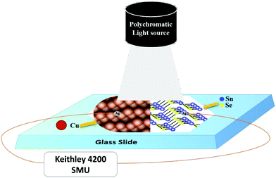 |
| | Fig. 1 Schematic diagram of the fabricated Cu/p-SnSe thin film. | |
3. Results and discussion
The elemental stoichiometry of the prepared SnSe thin film was confirmed using the EDAX technique. Fig. 2(a) shows the EDAX spectra of the SnSe thin film. The analysis of elements was carried out only for Sn and Se. The measured weight (%) of constituents is also tabulated as shown in the inset table in Fig. 2(a). The quantitative analysis of the spectrum shows that the atomic composition of the prepared SnSe films is near to stoichiometry. The XRD pattern of the as-grown tin selenide thin-film recorded at room temperature is shown in Fig. 2(b). The sharp peaks of the XRD pattern represent the highly crystalline nature of the SnSe thin film. The sharp peaks found within the pattern indicate the precise crystallinity of the samples with (400) as the dominant peak that is in agreement with the previously reported data.11,35 SnSe adopts an orthorhombic structure with layers belonging to the space group Pnma having lattice parameters a = 11.490 Å, b = 04.440 Å and c = 04.135 Å. Here, the obtained orthorhombic lattice system has a rectangular base that is formed by an orthogonal pair of lattice parameters a and b, onto which the layer growth takes place along the c direction. These mutually orthogonal a, b and c lattice parameters form a basic building block of the orthorhombic system that continued for long range order and hence the highly crystalline nature of the grown SnSe thin film is determined from the sharp peaks of the XRD result. The outcomes of XRD of the SnSe thin film are well-matched with the standard data (JCPDS card no. #48-1224) of SnSe. The structural parameters such as the crystallite size (t), dislocation density (δ) and micro strain (ε) are investigated and found to be 35.89 nm, 3.50 × 10⁸ (lin m−2) and 9.65 × 10⁻² (lin−2 m−4), respectively, for the most prominent peak (400). Similarly the values of the investigated structural parameters for other orientations are mentioned in the ESI† (Table S1).
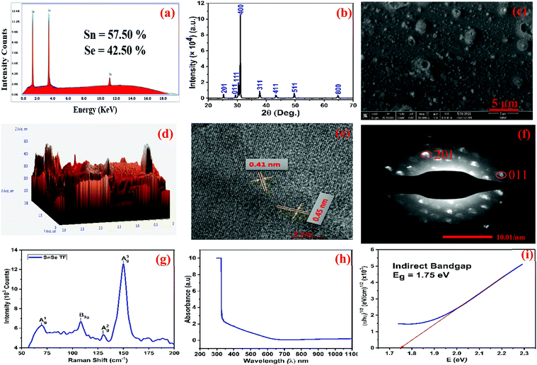 |
| | Fig. 2 (a) EDAX spectra of the SnSe thin-film. (b) X-Ray diffraction pattern of the SnSe thin film. (c) SEM images of the thin-film. (d) AFM 3D images of the thin film. (e) HR-TEM image and fringes of the SnSe thin film. (f) SAED spot pattern of the SnSe thin film. (g) Raman spectra of the SnSe thin film. (h) Absorption spectra vs. wavelength of the SnSe thin film. (i) Optical indirect band gap vs. photon energy (eV) of the SnSe thin film. | |
Scanning electron microscopy was employed to study the surface morphology of the as-deposited SnSe thin film. Fig. 2(c) shows the surface morphology and describes the continuity of this film. The AFM results demonstrated in Fig. 2(d) show the three-dimensional view of the deposited thin film.36–39 The optical microscopy images showing the SnSe and Cu Schottky diode are shown in the ESI† (Fig. S2). The structural determination of the SnSe thin films was also examined by HR-TEM as shown in Fig. 2(e), showing high and good crystalline order at the scale of the image of the measured thin film and giving an inter-planar spacing value of d[hkl] = 4.416 Å corresponding to the array of planes perpendicular to the films consistent with the SnSe thin film along the [400] direction. The inter-planar distance along the (011) plane was measured to be a lattice spacing of 0.41 nm and 0.45 nm that is assigned to the (011) crystalline plane of the SnSe thin film orthorhombic structure. Also one interesting feature is observed in the HR-TEM image that contains circular particle arrays as shown in the ESI† (Fig. S3). From this image, the particle size distribution is demonstrated by a histogram as shown in the ESI† (Fig. S4). The approximate lattice fringes correspond to an orthorhombic crystal structure, which is in agreement with a previous study.40 The corresponding selected area diffraction (SAED) pattern shown in Fig. 2(f) exhibits the good crystalline nature of the SnSe films. The SAED of a single-layer SnSe fragment exhibits an orthogonally symmetric diffraction pattern (Fig. 2(f)), indicating the single-crystalline nature of the film. In the SAED pattern, all the crystalline planes such as (201), (210), and (011) can be assigned to the orthorhombic crystal system of the space group Pcmn.40–45 Raman spectroscopy of the SnSe thin film was examined to characterize the lattice vibration modes and phase components in this sample. The spectra indicate four major vibrational modes at 70 cm−1, 107 cm−1, 130 cm−1, and 150 cm−1, with the peak at 107 cm−1 belonging to the B3g phonon mode and the other three peaks belonging to Ag phonon modes, as shown in Fig. 2(g). Ag and B3g are two stiff shear modes of a layer with regard to its neighbors in the b and c directions, which constitute the lattice's distinctive planar vibration modes.46,47 All of the measured vibrational modes match the typical modes of an orthorhombic structured SnSe thin film that is stable at room temperature. The absorbance spectra of the SnSe thin film deposited by the thermal evaporation technique on a glass substrate in the wavelength range of 300 nm to 1100 nm at room temperature are shown in Fig. 2(h). The band gap of the SnSe thin film can be determined by Tauc's equation using the following expression
where
A is the constant that comes from the Fermi-golden rules,
Eg is the band gap and
n depends on the type of band transition of the material.
48,49 The indirect band gap was calculated using the Tauc plot (for
n = ½) and found to be 1.75 eV. The optical band gap of the present work is compared with the previously reported data as shown in the ESI
† (Table S2).
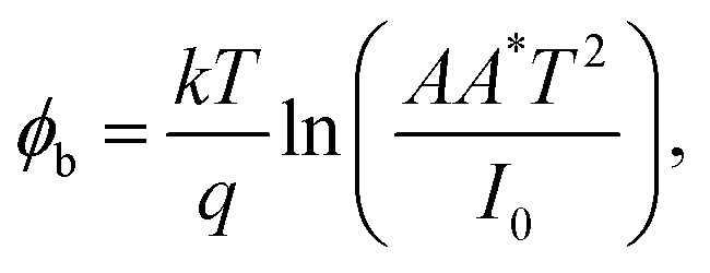
SEM analysis of the fabricated Schottky device was performed, and a cross sectional image of the device is shown in Fig. 3(a). According to the cross-sectional SEM results, the thickness of the manufactured device is 7.4 kÅ. Fig. 3(b) depicts the estimated band diagram, where ΦM is the work function of the Cu metal50 and χs is the electron affinity of SnSe51 and is 3.7 eV. Thus, from the Mott–Schottky theory, the ideal barrier height is given by Φb (eV) = ΦM (eV) − XS (eV), which is normally much lower in practical devices due to interface states and barrier inhomogeneity at the Cu/p-SnSe interface as shown in Fig. 3(b). The built-in voltage was calculated as Vbi = ΦM − ΦS, where ΦS is the work function of the semiconductor52 and is 3.94 eV.
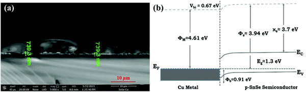 |
| | Fig. 3 (a) Cross sectional SEM image of the Cu/p-SnSe device. (b) Schematic diagram of the Cu/p-SnSe M–S thin film junction of the SBD. | |
4. Current–voltage (I–V) characteristics
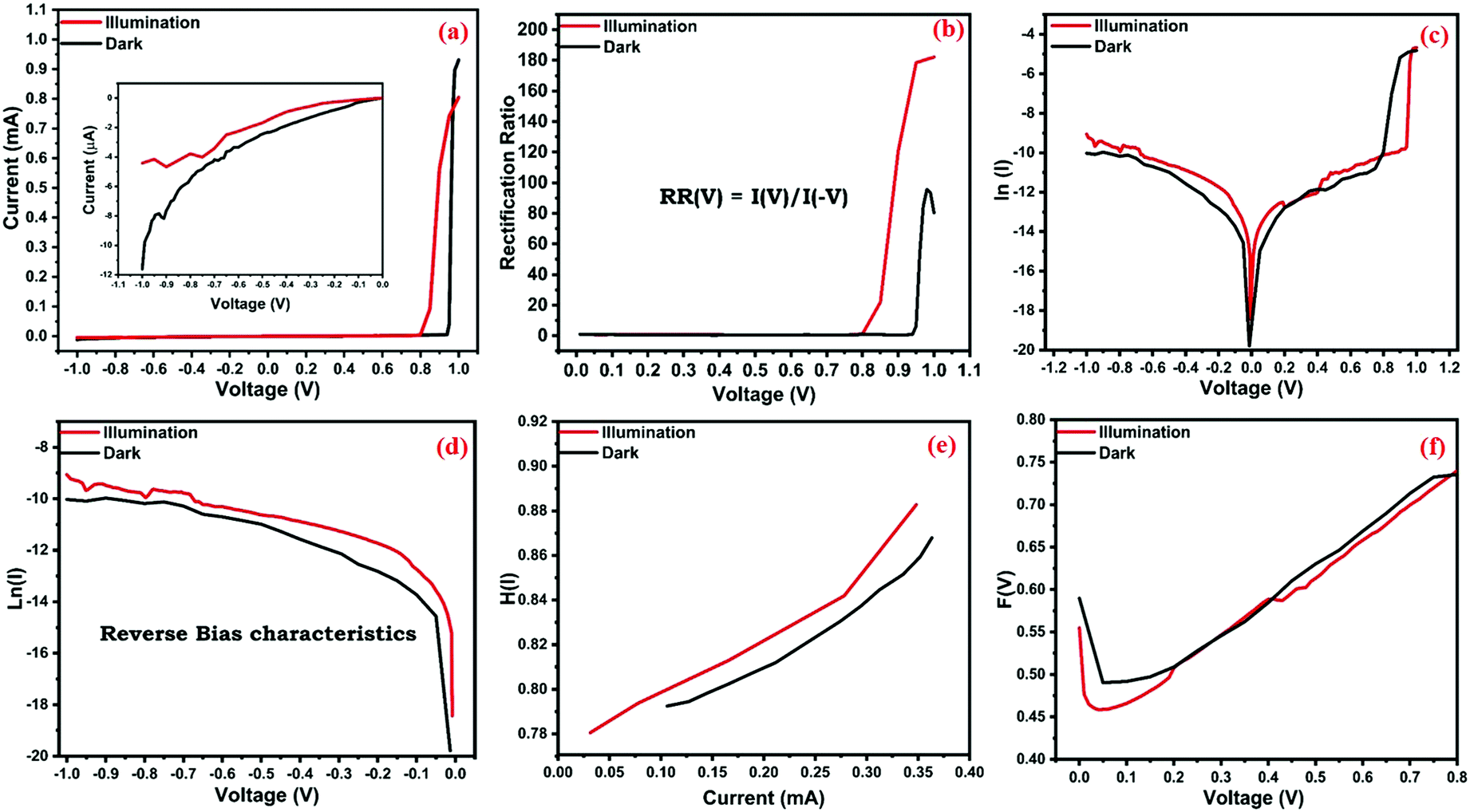
Fig. 4(a) depicts the current–voltage characteristics of a manufactured Schottky device under illumination and in the dark. According to Fig. 4(a), the device performance improves under illumination, indicating that the manufactured device is photosensitive.53–55
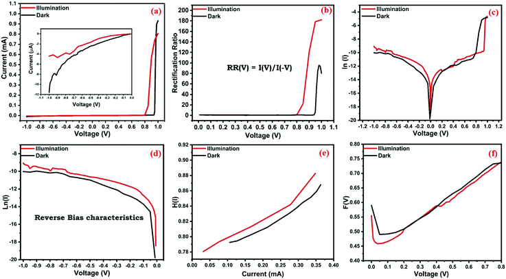 |
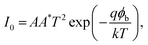
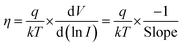
| | Fig. 4 (a) Current–voltage plot of the Cu/p-SnSe device under illumination and in the dark. (b) Rectification ratio of the Cu/p-SnSe device under illumination and in the dark. (c) ln(I) vs. V of the Cu/p-SnSe device under illumination and in the dark. (d) Reverse bias characteristics of the ln(I) vs. V method of the Cu/p-SnSe device under illumination and in the dark. (e) H(I) vs. I of the Cu/p-SnSe device under illumination and in the dark. (f) F(V) vs. V of the Cu/p-SnSe device under illumination and in the dark. | |
Here, the locally organized trap states/interface states that are constructed due to the mismatch of the lattice constants of SnSe and Cu as well as the existence of other impurities greatly affect the charge carrier flow across the interface. It is observed that the conductance mechanism follows thermionic emission theory for electron transport through the Schottky barrier.24 It is observed that the I–V performance of the device is enhanced under illumination, which is attributed to the optical band gap of the SnSe thin film in the visible range as well as the photosensitive nature of the fabricated device.
For large voltages, the rectification ratio, defined as the magnitude of the current ratio for positive and negative voltages, RR (V) = I(V)/I(−V), depends exponentially on voltage, like those in semiconductor diodes, and reaches absolutely enormous values.56 The nature of the maximum rectification ratio is shown in Fig. 4(b) and its values are found to be 97.63 and 182.11 in the dark and under illumination, respectively. Various device parameters are evaluated using several analytical methods from the recorded I–V data, such as the ln(I)–V technique, Cheung and Cheung function method and Norde's plot method. In the present study, the current–voltage (I–V) characteristics are used to define various Schottky diode parameters such as the saturation current, ideality factor, barrier height, and series resistance.
A graph on the logarithmic scale of current–voltage (I–V) giving a gamma shape curve was found and parameters such as the barrier height (Φb), saturation current (I0), and ideality factor (η) are calculated as shown in Fig. 4(c). After illuminating this device, the device performs effectively, and the saturation current, ideality factor and barrier height are improved, which indicates that the manufactured device exhibits enhanced photosensitivity. To determine the Schottky diode parameters thermionic emission (TE) theory is considered here.57–60 Using TE, the equation of the current flowing through the barrier is given below by eqn (2).
| |  | (2) |
where
I0 is
| |  | (3) |
I0 is the saturation current derived from the straight-line intercept of the ln(
I)–
V plot as shown in
Fig. 4(c),
V is the applied bias voltage across the junction barrier,
q is the electron charge,
k is the Boltzmann constant,
T is the absolute temperature in Kelvin,
A is the effective diode area, and
A* is the effective Richardson constant of 18 A cm
−2 K
−2 for p-SnSe from the study of N. Tugluoglu
et al.
61 The ideality factor
η of a diode from the supplied
eqn (4) is expressed as
| |  | (4) |
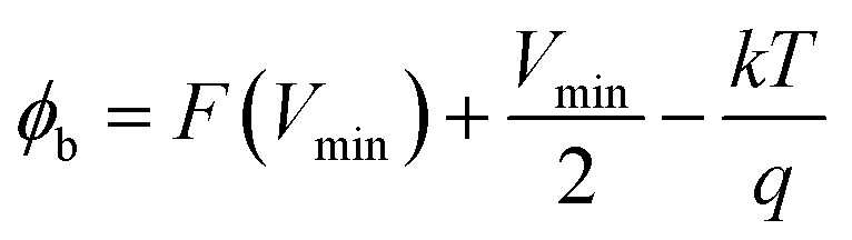
The ideality factor (η) may be calculated from the slope value of the lower forward bias area of V3kt/q. Here is a way to express the apparent barrier height Φb:
| |  | (5) |
where
Φb is the barrier height. A ln(
I)
vs. V plot of the Cu/p-SnSe M–S junction is shown in
Fig. 4(c). The logarithmic reverse and forward bias current–voltage characteristics of the Cu/p-SnSe Schottky barrier diode (SBDs) with illumination (polychromatic light) and without illumination (dark) are shown in
Fig. 4(d). It is observed that there is an increase in the leakage current when the device is placed under polychromatic light illumination. The values of the leakage current are −18.43 A and −19.78 A under polychromatic and dark conditions, respectively.
61
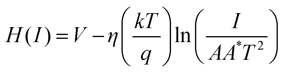
When the Cheung and Cheung function is plotted across current (I), the forward bias area again yields a straight line. H(I) denotes the Cheung and Cheung function, which is provided by eqn (6) expressed as
| | 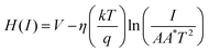 | (6) |
The straight-line equation is given by eqn (7) expressed as
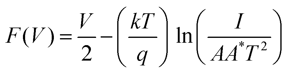
The forward characteristics of H(I) vs. I are shown in Fig. 4(e). The slope of the H(I) vs. I plot gives the series resistance Rs and the barrier height (Φb) can then be calculated as Φb = intercept/η, where the ideality factor is obtained from the ln(I) vs. V method used; there is another method to determine the value of the barrier height (Φb), which was proposed by Norde and known as the Norden method. When illuminating this device, the device functions well, with increased series resistance and barrier height, indicating that the constructed device is photosensitive. The updated Norde approach is expressed using eqn (8)
| |  | (8) |
| |  | (9) |
where
F(
V) is the Norden function. If
V = 3
kT/
q, IR is insignificant; thus the
F(
V)
versus V plot gives us a straight line with a slope of −1/2 and the intercept will give us the barrier height.
Eqn (9) predicts a straight line with a +1/2 slope when plotting
F(
V) against
V. A straight line is drawn on the
F(
V)
vs. V plot for the imposed forward bias. According to
eqn (10), it may be conceivable to calculate the lowest value of
F(
V) that will yield the barrier height (
Φb).
| |  | (10) |
where
F(
Vmin) = the value of
F(
V) at
Vmin.
The F(V) versus V plot for the Cu/p-SnSe thin-film device is shown in Fig. 4(f). When this device is illuminated, the device works well, with a higher barrier height, suggesting that the built device is considerably more sensitive. The obtained result we can see in Table 1 is the value of the Cu/p-SnSe thin film SBD parameter. Table 2 shows the SBD parameters in comparison to other metal/SnSe references. The Cu/SnSe interface with strong bonding has a certain tunneling barrier.62–69 The overall improvement in the Schottky barrier diode parameters due to illumination depicts its good photosensitive behavior and it should be considered for future optoelectronic applications.
Table 1 The parameters of the Cu/p-SnSe thin film SBD
| Device parameters |
Used method |
Illumination (polychromatic) |
Without illumination (dark) |
| Saturation current I0 (A) |
ln(I) vs. V method |
2.45 × 10⁻⁷ |
4.88 × 10⁻⁹ |
| Series resistance (kΩ) |
Modified Cheung and Cheung function |
17.61 |
33.67 |
| Ideality factor η |
ln(I) vs. V method |
1.38 |
1.58 |
|
|
ln(I) vs. V method |
0.40 |
0.50 |
| Barrier height Φb (eV) |
Modified Cheung and Cheung function |
0.42 |
0.66 |
|
|
Norden's plot method |
0.45 |
0.48 |
Table 2 The SBD parameters in comparison to other metal/SnSe references
| Sr. no. |
Schottky diode |
Device parameters |
Ref. |
| Barrier height Φb (eV) |
Ideality factor η |
| 1 |
In/p-SnSe |
1.828 |
0.420 |
22 |
| 2 |
Al/p-SnSe |
∼0.70 |
∼1.21 |
24 |
| 3 |
Ag/p-SnSe |
0.510 |
6.33 |
65 |
| 4 |
Ag/p-Sn0.2Se0.8 |
∼0.80 |
∼2.60 |
66 |
| 5 |
Cu/p-SnSe |
0.50 |
1.58 |
Present work |
| 6 |
Cu/p-SnSe (with illumination) |
0.40 |
1.38 |
5. Conclusions
SnSe charge was first grown using the DVT method, and subsequently its thin film was deposited using a thermal evaporation process. Energy dispersive X-ray analysis (EDAX) confirmed the stoichiometry of the elements of the as deposited thin film. By XRD analysis, it is found that the SnSe thin film exhibits higher crystallinity with orthorhombic lattice parameters of a = 11.490 Å, b = 4.440 Å and c = 4.135 Å. The optical band gap obtained from UV-Vis is 1.75 eV. The junction of a metal and a semiconductor is known as a metal–semiconductor junction of Cu/p-SnSe which is prepared by a thermal evaporation method. The current–voltage characteristics of a manufactured Schottky device are investigated under illumination and in the dark, demonstrating their photosensitive nature. The value of the ideality factor under dark conditions is 1.58, which decreases under illumination to 1.38. This exhibits enhanced device performance and demonstrates the manufactured diode's photosensitive nature. The Cu/p-SnSe Schottky diode's photosensitive feature can be useful in the development of future optoelectronic devices.
Author contributions
Hirenkumar Shantilal Jagani: conceptualization, writing – original draft, formal analysis, investigation, and methodology; Shubham Umeshkumar Gupta: writing – review and editing, validation, and visualization; Karan Bhoraniya: data curation and formal analysis; Mayuri Navapariya: data curation and formal analysis; Hetal Patel: formal analysis; Vivek M. Pathak: conceptualization, supervision, and validation; Gunvant K. Solanki: project administration, resources, supervision, and validation.
Conflicts of interest
There are no conflicts of interest to declare.
Acknowledgements
The author H. S. Jagani is thankful to Government of Gujarat for providing financial assistance under the SHODH scheme (Student Ref No: 201901640036). The authors highly acknowledge Prof. K. D. Patel, Department of Physics, Sardar Patel University, Gujarat, India, for useful discussion about the device physics of Schottky interfaces for device parameter investigation for the present article. The authors are also thankful to lab-mates Yash Joshi and Prachi Desai as well as Prof. M. P. Deshpande, Department of Physics, Sardar Patel University, Gujarat, India, for carrying out Raman spectroscopy measurements. The authors also show gratitude to Dr Swati J. Pandya, Department of Physics, Sardar Patel University, Gujarat, India, for providing UV-Vis-NIR spectroscopy measurements for the present work.
References
- R. Indirajith, T. P. Srinivasan, K. Ramamurthi and R. Gopalakrishnan, Synthesis, deposition and characterization of tin selenide thin films by thermal evaporation technique, Curr. Appl. Phys., 2010, 10(6), 1402–1406, DOI:10.1016/j.cap.2010.05.002.
- Y. Huang, L. Li, Y. H. Lin and C. W. Nan, Liquid Exfoliation Few-Layer SnSe Nanosheets with Tunable Band Gap, J. Phys. Chem. C, 2017, 121(32), 17530–17537, DOI:10.1021/acs.jpcc.7b06096.
- X. Wang, B. Liu, Q. Xiang, Q. Wang, X. Hou and D. Chen,
et al., Spray-painted binder-free SnSe electrodes for high-performance energy-storage devices, ChemSusChem, 2014, 7(1), 308–313, DOI:10.1002/cssc.201300241.
- S. U. Gupta, A. G. Dalvaniya, N. F. Patel, S. A. Bhakhar, S. Nair and J. Joy,
et al., Optical Switching Device Based on a Crystalline SnSe2 Photodetector in Diverse Conditions, ACS Appl. Electron. Mater., 2021, 3(11), 4859–4869, DOI:10.1021/acsaelm.1c00698.
- E. Y. A. Wornyoh, V. K. Jasti and C. F. Higgs, A review of dry particulate lubrication: Powder and granular materials, J. Tribol., 2007, 129(2), 438–449, DOI:10.1115/1.2647859.
- Q. Wang, W. Yu, X. Fu, C. Qiao, C. Xia and Y. Jia, Electronic and magnetic properties of SnSe monolayers doped by Ga, In, As, and Sb: A first-principles study, Phys. Chem. Chem. Phys., 2016, 18(11), 8158–8164, 10.1039/C5CP07111A.
- L. Dong, J. Lou and V. B. Shenoy, Large In-Plane and Vertical Piezoelectricity in Janus Transition Metal Dichalchogenides, ACS Nano, 2017, 11(8), 8242–8248, DOI:10.1021/acsnano.7b03313.
- M. R. Burton, C. A. Boyle, T. Liu, J. McGettrick, I. Nandhakumar and O. Fenwick,
et al., Full Thermoelectric Characterization of Stoichiometric Electrodeposited Thin Film Tin Selenide (SnSe), ACS Appl. Mater. Interfaces, 2020, 12(25), 28232–28238, DOI:10.1021/acsami.0c06026.
- W. Shi, M. Gao, J. Wei, J. Gao, C. Fan and E. Ashalley,
et al., Tin Selenide (SnSe): Growth, Properties, and Applications, Adv. Sci., 2018, 5(4), 1700602, DOI:10.1002/advs.201700602.
- M. Kumar, S. Rani, Y. Singh, K. S. Gour and V. N. Singh, Tin-selenide as a futuristic material: properties and applications, RSC Adv., 2021, 11(12), 6477–6503, 10.1039/D0RA09807H.
- K. Patel, G. Solanki, K. Patel, V. Pathak and P. Chauhan, Investigation of optical, electrical and optoelectronic properties of SnSe crystals, Eur. Phys. J. B, 2019, 92(9), 1–11, DOI:10.1140/epjb/e2019-100306-8.
- G. Duvjir, T. Min, T. Thi Ly, T. Kim, A. T. Duong and S. Cho,
et al., Origin of p-type characteristics in a SnSe single crystal, Appl. Phys. Lett., 2017, 110, 262106, DOI:10.1063/1.4991003.
- N. D. Boscher, C. J. Carmalt, R. G. Palgrave and I. P. Parkin, Atmospheric pressure chemical vapour deposition of SnSe and SnSe2 thin films on glass, Thin Solid Films, 2008, 516(15), 4750–4757, DOI:10.1016/j.tsf.2007.08.100.
- S. U. Gupta, A. G. Dalvaniya, C. Limberkar, K. D. Patel, G. K. Solanki and V. M. Pathak,
et al., Annealing induced phase transformation from amorphous to polycrystalline SnSe2 thin film photo detector with enhanced light–matter interaction, J. Non-Crystalline Solids, 2022, 578, 121353 CrossRef CAS , https://linkinghub.elsevier.com/retrieve/pii/S0022309321007146.
- Z. Zainal, N. Saravanan, K. Anuar, M. Z. Hussein and W. M. M. Yunus, Chemical bath deposition of tin selenide thin films, Mater. Sci. Eng., B, 2004, 107(2), 181–185, DOI:10.1016/j.mseb.2003.11.008.
- N. R. Mathews, Electrodeposited tin selenide thin films for photovoltaic applications, Sol. Energy, 2012, 86(4), 1010–1016, DOI:10.1016/j.solener.2011.06.012.
- C. Zhang, H. Li, Y. Su, Q. Zhang, Y. Li and J. Lu, Controllable and Versatile Electrophoretic Deposition Technology for Monolithic Organic Memory Devices, ACS Appl. Mater. Interfaces, 2020, 12(13), 15482–15490, DOI:10.1021/acsami.0c02190.
- E. E. Elemike, D. C. Onwudiwe, L. Wei, L. Chaogang and Z. Zhiwei, Noble metal–semiconductor nanocomposites for optical, energy and electronics applications, Sol. Energy Mater. Sol. Cells, 2019, 201, 110106, DOI:10.1016/j.solmat.2019.110106.
- L. Wind, M. Sistani, Z. Song, X. Maeder, D. Pohl and J. Michler,
et al., Monolithic Metal-Semiconductor-Metal Heterostructures Enabling Next-Generation Germanium Nanodevices, ACS Appl. Mater. Interfaces, 2021, 13(10), 12393–12399, DOI:10.1021/acsami.1c00502.
- N. Ben Saber, A. Mezni, A. Alrooqi and T. Altalhi, A review of ternary nanostructures based noble metal/semiconductor for environmental and renewable energy applications, J. Mater. Res. Technol., 2020, 9(6), 15233–15262, DOI:10.1016/j.jmrt.2020.10.090.
- F. F. Masouleh and N. Das, Application of Metal-Semiconductor–Metal Photodetector in High-Speed Optical Communication Systems, Adv. Opt. Commun., 2014, 84–114, DOI:10.5772/58997.
- H. Patel, K. Patel, A. Patel, H. S. Jagani, K. D. Patel and G. K. Solanki,
et al., Temperature-Dependent I–V Characteristics of In/p-SnSe Schottky Diode, J. Electron. Mater., 2021, 50(9), 5217–5225, DOI:10.1007/s11664-021-09043-y.
- N. Tuǧluoǧlu, S. Karadeniz, M. Şahin and H. Şafak, Temperature-dependent barrier characteristics of Ag/p-SnSe Schottky diodes based on I-V-T measurements, Semicond. Sci. Technol., 2004, 19(9), 1092–1097, DOI:10.1088/0268-1242/19/9/004.
- C. K. Sumesh, K. D. Patel and E. Menbari, Analysis of barrier height inhomogeneities in Al-pSnSe Schottky diode, Eur. Phys. J.: Appl. Phys., 2012, 59(2), 10103–p1-10103-p6, DOI:10.1051/epjap/2012120139.
- A. A. M. Farag, I. S. Yahia and M. Fadel, Electrical and photovoltaic characteristics of Al/n-CdS Schottky diode, Int. J. Hydrogen Energy, 2009, 34(11), 4906–4913, DOI:10.1016/j.ijhydene.2009.03.034.
- A. Shetty, B. Roul, S. Mukundan, L. Mohan, G. Chandan and K. J. Vinoy,
et al., Temperature dependent electrical characterisation of Pt/HfO2/n-GaN metal-insulator-semiconductor (MIS) Schottky diodes, AIP Adv., 2015, 5(9), 097103, DOI:10.1063/1.4930199.
- I. Hussain, M. Y. Soomro, N. Bano, O. Nur and M. Willander, Systematic study of interface trap and barrier inhomogeneities using I-V-T characteristics of Au/ZnO nanorods Schottky diode, J. Appl. Phys., 2013, 113(23), 234509, DOI:10.1063/1.4810924.
- S. K. Tripathi and M. Sharma, Analysis of the forward and reverse bias I-V and C-V characteristics on Al/PVA: n-PbSe polymer nanocomposites Schottky diode Analysis of the forward and reverse bias I-V and C-V characteristics on Al/PVA: n-PbSe polymer nanocomposites, J. Appl. Phys., 2012, 111(7), 074513, DOI:10.1063/1.3698773.
- M. Sharma and S. K. Tripathi, Study of barrier inhomogeneities in I–V-T and C-V-T characteristics of Al/Al2O3/PVA: n-ZnSe metal–oxide–semiconductor diode Study of barrier inhomogeneities in I–V-T and C-V-T characteristics of Al/Al2O3/PVA: n-ZnSe metal–oxide–semiconductor diode, J. Appl. Phys., 2012, 112(2), 024521, DOI:10.1063/1.4737589.
- S. W. King, M. French, M. Jaehnig, M. Kuhn, B. Boyanov and B. French,
et al., X-ray photoelectron spectroscopy measurement of the Schottky barrier at the SiC (N)/Cu interface X-ray photoelectron spectroscopy measurement of the Schottky barrier at the SiC (N)/Cu interface, J. Vac. Sci. Technol., B, 2011, 29(5), 051207, DOI:10.1116/1.3633691.
- S. Chand and J. Kumar, Effects of barrier height distribution on the behavior of a Schottky diode, J. Appl. Phys., 1997, 82(10), 5005, DOI:10.1063/1.366370.
- A. Kumar, S. Arafin, M. C. Amann and R. Singh, Temperature dependence of electrical characteristics of Pt/GaN Schottky diode fabricated by UHV e-beam evaporation, Nanoscale Res. Lett., 2013, 8, 481, DOI:10.1186/1556-276X-8-481.
- D. Sahoo, P. Priyadarshini, A. Aparimita, D. Alagarasan, R. Ganesan and S. Varadharajaperumal,
et al., Role of annealing temperature on optimizing the linear and nonlinear optical properties of As40Se50Ge10films, RSC Adv., 2020, 10(45), 26675–26685, 10.1039/D0RA04763E.
- A. Patel, V. M. Pathak, G. K. Solanki, K. D. Patel and P. Pataniya, The influence of antimony doping on I–V, C–V-f and (G/w)-V-f characteristics of indium/SbXW1-XSe2 (X = 0, 0. 1, 0.5) alloy Schottky diodes, Superlattices Microstruct., 2020, 137, 106348, DOI:10.1016/j.spmi.2019.106348.
- M. R. Pallavolu, V. R. Minnam Reddy, P. R. Guddeti and C. Park, Development of SnSe thin films through selenization of sputtered Sn-metal films, J. Mater. Sci.: Mater. Electron., 2019, 30(17), 15980–15988, DOI:10.1007/s10854-019-01968-9.
- P. Chauhan, A. B. Patel, G. K. Solanki, K. D. Patel, V. M. Pathak and C. K. Sumesh,
et al., Rhenium substitutional doping for enhanced photoresponse of n-SnSe2/p-Si heterojunction based tunable and high-performance visible-light photodetector, Appl. Surf. Sci., 2021, 536, 147739, DOI:10.1016/j.apsusc.2020.147739.
- R. Indirajith, M. Rajalakshmi, R. Gopalakrishnan and K. Ramamurthi, Effects of annealing on thermally evaporated SnSe thin films, Ferroelectrics, 2011, 413(1), 108–114, DOI:10.1080/00150193.2011.551090.
- I. Y. Ahmet, M. S. Hill, P. R. Raithby and A. L. Johnson, Tin guanidinato complexes: Oxidative control of Sn, SnS, SnSe and SnTe thin film deposition, Dalton Trans., 2018, 47(14), 5031–5048, 10.1039/C8DT00773J.
- Ş. Ţălu, S. Solaymani, S. Rezaee and N. B. Nezafat, The evaluation of surface topography changes in nanoscaled 2,6-diphenyl anthracene thin films by atomic force microscopy, Microsc. Res. Tech., 2021, 84(1), 89–100, DOI:10.1002/jemt.23569.
- A. You, B. May and I. In, Solid-to-solid phase transformations of nanostructured selenium-tin thin films induced by thermal annealing in oxygen atmosphere, AIP Conf. Proc., 2014, 1603(1), 31, DOI:10.1063/1.4883039.
- K. S. Hingarajiya, K. D. Patel and G. K. Solanki, Structural and Optical Characterization of Nanocrystalline SnSe Thin Film, Int. J. Res. Sci. Innov. Appl. Sci., 2016, I(Viii), 6–11 Search PubMed.
- J. A. Hernandez, A. Ruiz, L. F. Fonseca, M. Jose-yacaman, A. Benitez and M. T. Pettes, Thermoelectric properties of SnSe nanowires with different diameters, Sci. Rep., 2018, 8, 11966, DOI:10.1038/s41598-018-30450-5.
- X. Shi, X. Tao, J. Zou and Z. Chen, High-Performance Thermoelectric SnSe: Aqueous Synthesis, Innovat. Challen., 2020, 7(7), 1902923, DOI:10.1002/advs.201902923.
- X. Gong, H. Wu, D. Yang, B. Zhang, K. Peng and H. Zou,
et al., Temperature dependence of Raman scattering in single crystal SnSe, Vib. Spectrosc., 2020, 107, 103034, DOI:10.1016/j.vibspec.2020.103034.
- J. Jiang, C. Pei, Y. Wong, W. Zhang, A. Thye and S. Wee, Atmospheric Pressure Fabrication of Large-Sized Single-Layer Rectangular SnSe Flakes, J. Vis. Exp., 2018, 133, 57023, DOI:10.3791/57023.
- Y. Feng, X. Zhang, L. Lei, Y. Nie and G. Xiang, Rapid synthesis of thermoelectric SnSe thin films by MPCVD, RSC Adv., 2020, 10(20), 11990–11993, 10.1039/D0RA01203C.
- H. R. Chandrasekhar, R. G. Humphreys, U. Zwick and M. Cardona, Infrared and Raman spectra of the IV-VI compounds SnS and SnSe, Phys. Rev. B: Solid State, 1977, 15(4), 2177–2183, DOI:10.1103/PhysRevB.15.2177.
- A. R. Wassel and IM El. Radaf, Synthesis and characterization of the chemically deposited - SnS1−x - Sex thin films: structural, linear and nonlinear optical properties, Appl. Phys. A, 2020, 126, 177, DOI:10.1007/s00339-020-3353-7.
- Z. Li, Y. Guo, F. Zhao, C. Nie, H. Li and J. Shi,
et al., Effect of film thickness and evaporation rate on co-evaporated SnSe thin films for photovoltaic applications, RSC Adv., 2020, 10(28), 16749–16755, 10.1039/D0RA01749C.
- E. W. J. Mitchell and J. W. Mitchell, The Work Functions of Copper, Silver and Aluminium, Proc. R. Soc. A, 1951, 210(1100), 70–84, DOI:10.1098/rspa.1951.0231.
- H. S. Im, Y. Myung, Y. J. Cho, C. H. Kim, H. S. Kim and S. H. Back,
et al., Facile phase and composition tuned synthesis of tin chalcogenide nanocrystals, RSC Adv., 2013, 3(26), 10349–10354, 10.1039/C3RA40869H.
- Z. Cui, X. Wang, Y. Ding and M. Li, Exploration work function and optical properties of monolayer SnSe allotropes, Superlattices Microstruct., 2018, 114, 251–258, DOI:10.1016/j.spmi.2017.12.039.
- S. Gunasekaran, D. Thangaraju, R. Marnadu, J. Chandrasekaran, M. Shkir and A. Durairajan,
et al., Photosensitive activity of fabricated core-shell composite nanostructured p-CuO@CuS/n-Si diode for photodetection applications, Sens. Actuators, A, 2021, 317, 112373, DOI:10.1016/j.sna.2020.112373.
- Y. Wu, L. Liu, W. Wang, W. Zhang, H. Yu and J. Qian,
et al., Enhanced stability and performance of light-emitting diodes based on: In situ fabricated FAPbBr3 nanocrystals via ligand compensation with n-octylphosphonic acid, J. Mater. Chem. C, 2020, 8(29), 9936–9944, 10.1039/D0TC01694B.
- T. He, C. Lan, S. Zhou, Y. Li, Y. Yin, C. Li and Y. Liu, Enhanced responsivity of a graphene/Si-based heterostructure broadband photodetector by introducing a WS2 interfacial layer, J. Mater. Chem. C, 2021, 9(11), 3846–3853, 10.1039/D0TC05796G.
- S. Sherif, G. Rubio-Bollinger, E. Pinilla-Cienfuegos, E. Coronado, J. C. Cuevas and N. Agraït, Current rectification in a single molecule diode: The role of electrode coupling, Nanotechnology, 2015, 26(29), 1–11, DOI:10.1088/0957-4484/26/29/291001.
- I. S. Yahia, A. A. M. Farag, F. Yakuphanoglu and W. A. Farooq, Temperature dependence of electronic parameters of organic Schottky diode based on fluorescein sodium salt, Synth Met., 2011, 161(9–10), 881–887, DOI:10.1016/j.synthmet.2011.02.016.
- M. K. Hudait, P. Venkateswarlu and S. B. Krupanidhi, Electrical transport characteristics of Au/n-GaAs Schottky diodes on n-Ge at low temperatures, Solid-State Electron., 2001, 45, 133–141, DOI:10.1016/S0038-1101(00)00230-6.
- D. A. Aldemir, A. Kökce and A. F. Özdemir, The comparison of the methods used for determining of Schottky diode parameters in a wide temperature range Schottky diyot parametrelerini belirlemede kullanılan metotların geniş bir sıcaklık aralığı için kıyaslanması, Sakarya University Journal of Science, 2017, 21(6), 1286–1292, DOI:10.16984/saufenbilder.279996.
- V. L. Devi, I. Jyothi, V. R. Reddy and C. Choi, Schottky Barrier Parameters and Interfacial Reactions of Rapidly Annealed Au/Cu Bilayer Metal Scheme on N-type InP, Open Appl. Phys. J., 2012, 5, 1–9, DOI:10.2174/1874183501205010001.
- N. Tu, Temperature-dependent barrier characteristics of Ag/p-SnSe Schottky diodes based on I–V–T measurements, Institute of Physics Publishing: Semiconductor Science and Technology, 2004, 19(9), 1092, DOI:10.1088/0268-1242/19/9/004.
- I. I. Nedrygailov, Y. Heo, H. Kim and J. Y. Park, Charge Transfer during the Aluminum-Water Reaction Studied with Schottky Nanodiode Sensors, ACS Omega, 2019, 4(24), 20838–20843, DOI:10.1021/acsomega.9b03397.
- C. He, M. Cheng, T. Li and W. Zhang, Tunable Ohmic, p-Type Quasi-Ohmic, and n-Type Schottky Contacts of Monolayer SnSe with Metals, ACS Appl. Nano Mater., 2019, 2(5), 2767–2775, DOI:10.1021/acsanm.9b00276.
- G. A. Saenz, G. Karapetrov, J. Curtis and A. B. Kaul, Ultra-high photoresponsivity in suspended metal-semiconductor-metal mesoscopic multilayer MoS2 broadband detector from UV-to- IR with low Schottky barrier contacts, Sci. Rep., 2018, 8(1), 1–11, DOI:10.1038/s41598-018-19367-1.
- T. Shen, J. C. Ren, X. Liu, S. Li and W. Liu, van der Waals Stacking Induced Transition from Schottky to Ohmic Contacts: 2D Metals on Multilayer InSe, J. Am. Chem. Soc., 2019, 141(7), 3110–3115, DOI:10.1021/jacs.8b12212.
- J. You, C. Si, J. Zhou and Z. Sun, Contacting MoS2 to MXene: Vanishing p-Type Schottky Barrier and Enhanced Hydrogen Evolution Catalysis, J. Phys. Chem. C, 2019, 123(6), 3719–3726, DOI:10.1021/acs.jpcc.8b12469.
- W. Zhou, Y. Guo, J. Liu, F. Q. Wang, X. Li and Q. Wang, 2D SnSe-based vdW heterojunctions: Tuning the Schottky barrier by reducing Fermi level pinning, Nanoscale, 2018, 10(28), 13767–13772, 10.1039/C8NR02843E.
- H. Şafak, M. Şahin and Ö. Faruk Yüksel, Analysis of I-V measurements on Ag/p-SnS and Ag/p- SnSe Schottky barriers, Solid-State Electron., 2002, 46(1), 49–52, DOI:10.1016/S0038-1101(01)00273-8.
- K. K. Patel, M. Patel, K. D. Patel, G. K. Solanki, V. M. Pathak and R. Srivastava, Temperature Dependent I–V Characteristics Of Ag/p-Sn0.2Se0.8 Thin Film Schottky Barrier Diode, J. Nano-Electron. Phys., 2011, 3, 783–786 Search PubMed.
Footnote |
| † Electronic supplementary information (ESI) available: Table S1 presents the crystallographic parameters of the SnSe thin film obtained from XRD. Fig. S1 presents the optical image of the Schottky diode using an optical microscope having a magnification of 10×. Fig. S2 presents the HR-TEM image of the SnSe thin film deposited on the NaCl crystal. Fig. S3 presents the histogram of the HR-TEM image of the size distribution of nanoparticles of the SnSe thin film. Table S2 compares the present work with previously reported data. See DOI: 10.1039/d1ma01005k |
|
| This journal is © The Royal Society of Chemistry 2022 |
Click here to see how this site uses Cookies. View our privacy policy here. 
 Open Access Article
 This Open Access Article is licensed under a Creative Commons Attribution-Non Commercial 3.0 Unported Licence
 *,
Shubham Umeshkumar
Gupta
*,
Shubham Umeshkumar
Gupta