
 Open Access Article
 This Open Access Article is licensed under a
 Creative Commons Attribution 3.0 Unported Licence
Flexible and ultra-thin silver films with superior electromagnetic interference shielding performance via spin-coating silver metal–organic decomposition inks†
Jingyuan
Zhang
ab,
Xiaodong
Li
 *ab,
Mu
Zhang
ab,
Qi
Zhu
ab and
Xudong
Sun
ab
*ab,
Mu
Zhang
ab,
Qi
Zhu
ab and
Xudong
Sun
ab
aKey Laboratory for Anisotropy and Texture of Materials (Ministry of Education), Northeastern University, Shenyang, Liaoning 110819, China. E-mail: xdli@mail.neu.edu.cn
bResearch Center for Advanced Ceramic Materials, School of Materials Science and Engineering, Northeastern University, Shenyang, Liaoning 110819, China
First published on 11th November 2021
Abstract
Herein, we present a clean, green and economical method to prepare flexible and ultrathin silver films for electromagnetic interference (EMI) shielding by thermal decomposition of metal–organic decomposition (MOD) inks. The non-particulate ink synthesized by complexing silver oxalate with 1,2-diaminopropane in ethanol solvent can be easily decomposed to pure silver at a quite low temperature in air. The efficient electrical transport network constructed by the interconnected nanoparticles of the silver film results in outstanding electrical properties and shielding performance, with an absorption-dominated mechanism. By curing the ink at 130 °C for 30 min, a more effective network structure for electron transport can be obtained. By the spin coating deposition method, the silver film with only a 200 nm thickness has an ultrahigh conductivity of 8.46 × 10⁶ S m−1 and excellent shielding effectiveness of 51.1 dB at 10.3 GHz in the X band, which is the highest shielding effectiveness of the film with such thin thickness so far. The factors affecting the EMI shielding performance of silver films were elucidated, including the heat treatment process, ink concentration and spin coating times, and the relationship between the microstructure and the properties of the film was established. This work indicates that silver metal–organic decomposition inks will be a favorable choice for the industrial production of EMI shielding applications.
1. Introduction
In recent years, the rapid development of electronic equipment and wireless communication technology has brought about a serious electromagnetic radiation pollution problem to operational electronic devices and human health. To mitigate this pollution problem, electromagnetic interference (EMI) shielding materials have attracted growing attention. So far, the mainly developed electromagnetic shielding materials are conductive materials, including metal-based materials,1,2 carbon-based materials,3,4 conductive polymers5,6 and MXenes.7 Among them, metals are mostly used for EMI shielding applications due to their abundant free electrons and ultrahigh conductivity, which can reflect electromagnetic waves effectively. However, their shortcomings, like heaviness, poor flexibility and difficult processability, limit their usage in modern electronic equipment. Hence, besides the high shielding effectiveness (SE), new requirements for metal-based electromagnetic shielding materials are put forward, such as lightness, flexibility, and ultra-thin thickness.8–11 Particularly, in the integrated circuit chip industry, conformal self-EMI shielding is proposed by preparing a seamless metallic shielding layer on the molding compound to alternate the traditional metallic cans. Nowadays, different types of coating processes have been developed for conformal self-EMI shielding with a thickness of several microns, such as sputtering,12 spraying,13 plating14–16 and jet dispensing.17 For example, the electromagnetic shielding effectiveness of the film prepared by jet dispensing silver conductive ink with a thickness of 20 μm can reach 60–85 dB at 1.6–2.6 GHz.17 It is of great significance for conformal shielding to develop ultra-thin silver films by a facile and economic method.Recently, Jia et al. dispersed Ag flakes into water with waterborne polyurethane (WPU) and a fluorocarbon surfactant to obtain a conductive ink.18 The obtained Ag/WPU coating with a thickness of 10 μm had high conductivity (14![[thin space (1/6-em)]](https://www.rsc.org/images/entities/char_2009.gif) 300 S cm−1) and shielding effectiveness (74.5 dB), demonstrating that conductive inks have many advantages in electromagnetic shielding applications. Generally, conductive inks can be applied to additive manufacturing for various printing and coating technologies to achieve large-scale production.19–21 However, due to the poor stability of conductive particle inks, surfactants are needed to disperse the particles into the solvent, which requires a high thermal temperature to remove.22,23 Furthermore, for inkjet printing, particle inks can result in a clogged nozzle easily. Therefore, it is urgent to develop a stable and particle free conductive ink suitable for electromagnetic shielding materials and optimize its preparation process to understand the relationship between its microstructure and properties. The metal–organic decomposition (MOD) ink of silver carboxylates and amine in an ethanol solvent was stable in air for several months.24,25 Pure-phase silver films can be obtained via the thermal decomposition of this non-particulate ink at a quite low temperature in air, which is a clean and energy-saving method with high utilization of silver. The silver film thermally treated at 150 °C for 30 min has low resistivity (8.6 μΩ cm),24 demonstrating that it may be a potential candidate for the next generation of electromagnetic shielding materials.
300 S cm−1) and shielding effectiveness (74.5 dB), demonstrating that conductive inks have many advantages in electromagnetic shielding applications. Generally, conductive inks can be applied to additive manufacturing for various printing and coating technologies to achieve large-scale production.19–21 However, due to the poor stability of conductive particle inks, surfactants are needed to disperse the particles into the solvent, which requires a high thermal temperature to remove.22,23 Furthermore, for inkjet printing, particle inks can result in a clogged nozzle easily. Therefore, it is urgent to develop a stable and particle free conductive ink suitable for electromagnetic shielding materials and optimize its preparation process to understand the relationship between its microstructure and properties. The metal–organic decomposition (MOD) ink of silver carboxylates and amine in an ethanol solvent was stable in air for several months.24,25 Pure-phase silver films can be obtained via the thermal decomposition of this non-particulate ink at a quite low temperature in air, which is a clean and energy-saving method with high utilization of silver. The silver film thermally treated at 150 °C for 30 min has low resistivity (8.6 μΩ cm),24 demonstrating that it may be a potential candidate for the next generation of electromagnetic shielding materials.
In this work, we introduced a silver MOD ink to prepare flexible silver films of ultra-thin thickness for electromagnetic shielding applications. The silver MOD inks in this work were synthesized by complexing silver oxalate powder with 1,2-diaminopropane. The wet films deposited by the spin coating method were cured at different temperatures and times. The effects of the heat treatment process on the microstructure, conductivity and electromagnetic shielding properties of the films were analyzed. The electromagnetic shielding mechanism of the nanoparticle silver film was also explained. In addition, the thickness of the film was altered by changing the ink concentration and spin coating times, and their effects on the microstructure, electrical properties and electromagnetic shielding performance of the film were explored. Finally, the relationships between the microstructure, electrical properties and electromagnetic shielding properties of silver films were established.
2. Experimental
2.1 Materials
Silver nitrate was purchased from Sino-platinum Metals Co. Ltd. Sodium oxalate and ethanol were purchased from Sinopharm Chemical Reagent Co. Ltd. 1,2-Diaminopropane and ethyl cellulose were purchased from Aladdin Industrial Corp. All the reagents were of analytical grade and used without further purification. Polyethylene terephthalate films (PET) with a thickness of 0.4 μm used here were purchased from Du Pont Co Ltd.2.2 Preparation of silver MOD inks and films
First, silver oxalate powder was synthesized by the ion-exchange reaction between silver nitrate and sodium oxalate, according to a procedure in our previous work.24 Then, a mixture of ethanol, 1,2-diaminopropane, ethyl cellulose ethoce and silver oxalate powder was constantly stirred until all the mass was fully dissolved and a transparent ink was obtained. Finally, the ink was filtered through a 0.22 μm syringe filter and then stored in a refrigerator for the following use. For preparing different concentrations of the ink, we dissolved different amounts of silver oxalate powder in 1 ml of ethanol. For example, 1 mmol silver oxalate powder was prepared for a 1 M ink.The 3 cm × 3 cm PET films used as the substrates were cleaned with ethanol and deionized water, followed by O2 plasma treatment to achieve hydrophilic surfaces.26 The prepared MOD ink was spin-coated on the pretreated PET substrate at 3000 rpm for 20 s to obtain wet films. Then, the wet films were thermally treated on a hotplate at different temperatures and times. For films with multilayers, spin-coating and thermal treatment were repeated several times and the repeated times corresponded to the film layers.
2.3 Characterization
Thermogravimetric analysis and differential scanning calorimetry (TG-DSC) were carried out with a simultaneous thermal analyzer (STA 449F3, Netzsch Co., German) at a heating rate of 10 °C min−1 under air. X-Ray diffraction (XRD) analysis was performed by using nickel-filtered Cu-Kα radiation under 40 kV/200 mA (SmartLab, Rigaku, Japan). The surface morphologies of the silver films were observed by field emission scanning electron microscopy (FE-SEM) with an acceleration voltage of 15 kV (Model JSM-7001F, JEOL, Japan). The thickness of the film was measured from the SEM photographs of cross-sectional images with an 80° tilt. The inks thermolyzed at various temperatures were investigated by Fourier transform infrared spectroscopy (FTIR, Spectrum RXI, PerkinElmer, USA) using the standard KBr method. Atomic force microscopy (CSPM5500, Benyuan Corporation, China) and confocal laser scanning microscopy (OLS3100, Olympus, Japan) were used to detect the film surfaces and calculate the root mean square (RMS) roughness of the silver films. The sheet resistance of the film was measured using a four-point probe system (RST-8, Guangzhou Four-Point Probe Technology Co., Ltd, China).The EMI shielding performance was analyzed using a vector network analyzer (VNA, Keysight N5222A, USA) in the frequency range of 8.2–12.4 GHz (X band). Before testing, the films were cut to suit the waveguide sample holder. After the measurement, the S parameters (S11, S12, S21, and S22) were collected to calculate the power coefficients (R, A, and T) and shielding effectiveness (SER, SEA, and SET) according to the following equations.27,28
| R = |S11|2 = |S22|2 | (1) |
| T = |S12|2 = |S21|2 | (2) |
| A = 1 − R − T | (3) |
| SER = −10log(1 − R) | (4) |
| SEA = −10log(T/1 − R) | (5) |
| SET = SER + SEA (when SER ≥ 10 dB) | (6) |
3. Results and discussion
3.1 Effects of thermal treatment on the microstructure and properties of the films
Fig. 1a and b show the images of the prepared silver MOD ink and the silver film. The ink with 24.5 wt% of solid content exhibits a clear and transparent appearance with no particles, as also confirmed by UV-Vis absorption analysis (Fig. S1, ESI†). The PET substrates spin-coated with the silver ink and heat-treated at 130 °C show the luster of silver metal and were flexible with bending. According to previous studies, the heat treatment process plays an important role in the microstructure and properties of silver films derived from MOD inks.24,29–32 Prior to drafting the thermal treatment process, the thermal decomposition behaviors of the silver oxalate-1,2-diaminopropane ink were investigated. TG-DSC thermal analysis was carried out and the results are shown in Fig. 1c. The thermal decomposition process of the ink ended before 170 °C and can be divided into three steps. The first step is from room temperature to 105 °C, during which the mass fraction of the ink decreased by ∼40%, accompanied by an obvious endothermic peak at 97.7 °C in the DSC curve. This decomposition process is caused by the volatilization of the solvent. The second decomposition process started at 105 °C and ended at 135 °C, with a 20% mass loss and an endothermic peak at 115.5 °C in the DSC curve. This step corresponds to the decomposition of the silver–amine complex and the volatilization of 1,2-diaminopropane. In the last step, from 135 °C to 152 °C, the mass fraction of the ink decreased to 17.3%, and a strong endothermic peak appeared at 149.5 °C in the DSC curve, corresponding to the decomposition of the remaining organic matter in the ink. Finally, the mass was stable at 16.9%, representing the mass fraction of silver in the ink. Accordingly, the temperature range of the heat treatment process for the ink is set as 90–170 °C and six films heat-treated at different temperatures were fabricated.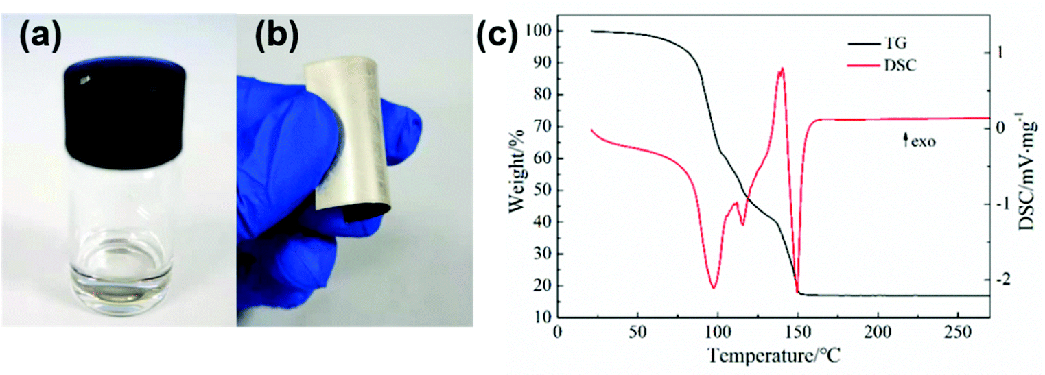 | ||
| Fig. 1 (a) Image of silver oxalate-1,2-diaminopropane ink, (b) image of the silver film, and (c) the TG-DSC curve of the ink. | ||
The SEM images (Fig. 2a1–a6) show that the film is composed of interconnected nanoscale Ag particles with some pores among them. The ink all turned into pure silver in the whole temperature range investigated, as seen from the XRD patterns (Fig. 2b) of the six fabricated films. The intensity of the peaks gradually increased with the increase of the curing temperature, corresponding to the increased crystallite size and the growing amount of decomposed silver in the film. The nanoparticles of silver are less than 100 nm, hence, the grain size of Ag films can be calculated by the Scherrer formula according to the XRD data, as shown in Fig. 2c. The grain size gradually increases with the temperature from 16 nm at 90 °C to 25 nm at 150 °C, afterwards becoming stable at 25 nm. It can be concluded that the internal microstructure of the film is a nanonetwork structure composed of more than 20 nanometer sized silver particles with a large number of pores. Although the porosity of the film is very small, nanometer-sized pores are dispersed among the nanoparticles, resulting in a large number of interfaces among the particles in the film. To further explore the residual organic matter in the films, FT-IR analysis was performed on the above films, as shown in Fig. 2d. In the FTIR spectrum of the ink, the broad and strong band at 3700–3020 cm−1 is originated from the O–H bond of ethanol and the amine group of the complexing agent 1,2-diaminopropane.24 The absorption band at 2980–2860 cm−1 corresponds to the C–H stretching vibration of the organic solvent.24 The peaks between 1760 cm−1 and 1240 cm−1 are attributed to the stretching vibration of the amine group and carbonyl in oxalate.33,34 After heat treatment at 90 °C for 30 min, the broad FTIR spectrum of the product turned into a strong and sharp peak at 3306 cm−1, which is the vibration peak of the amine group,24 indicating that the ethanol solvent had volatilized and 1,2-diaminopropane remained in the decomposition product of the ink. A large number of sharp peaks appear at 1760–1240 cm−1, also indicating that 1,2-diaminopropane and oxalate remained and were wrapped on the surface of the silver nanoparticles. The small peak at 2210 cm−1, corresponding to carbon oxide,35 is likely due to oxalate partially decomposing into CO2 and adsorbing on the decomposition products. As the temperature was increased to 100 °C, the peak at 3306 cm−1 disappeared, indicating that 1,2-propanediamine had volatilized. In the local expansion of the FTIR spectrum (shown as Fig. S2, ESI†), two weak peaks are found at 1383 cm−1 and 2168 cm−1, corresponding to the symmetric stretching vibration of carboxylate36 and CO adsorbed on the product surface, respectively. With the increase in temperature, the intensity of the two remaining peaks decreased gradually. When the temperature was increased to 170 °C, no peak was found. Therefore, the FTIR results, being consistent with the TG-DSC analysis, suggest that the residual organic matter decomposes more thoroughly with the increase of curing temperature and there is almost no organic matter in the film at 170 °C.
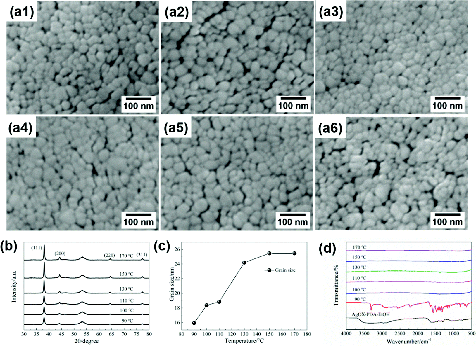 | ||
| Fig. 2 Characterization of films thermally treated at different temperatures. (a1–a6) SEM images. (a1) 90 °C, (a2) 100 °C, (a3) 110 °C, (a4) 130 °C, (a5) 150 °C, and (a6) 170 °C. (b) XRD patterns, (c) grain size and (d) FTIR spectrum. | ||
The electrical conductivity of the films cured at different temperatures is shown in Fig. 3a. The conductivity increases with the increase of curing temperature, attributed to more contact of the particles and less porosity of the films, which is a result of the decomposition degree of the ink. The formed nanoparticles at 90 °C are wrapped with the undecomposed ink, which blocks the conductive path. On the other hand, the film cured at 170 °C completely decomposed with the largest grain size and the smallest porosity, forming the most effective electron transport network structure. Therefore, it has the largest conductivity of up to 8.76 × 10⁶ S m−1, which is close to the conductivity of bulk silver (6.3 × 10⁷ S m−1). The same analysis methods were applied to the films cured for different times ranging from 1 min to 60 min and similar results (Fig. S3a–d, ESI†) can be seen with extension of the curing time, the grain size of the silver films is enhanced, while the porosity is reduced, and thereby, the conductivity is improved.
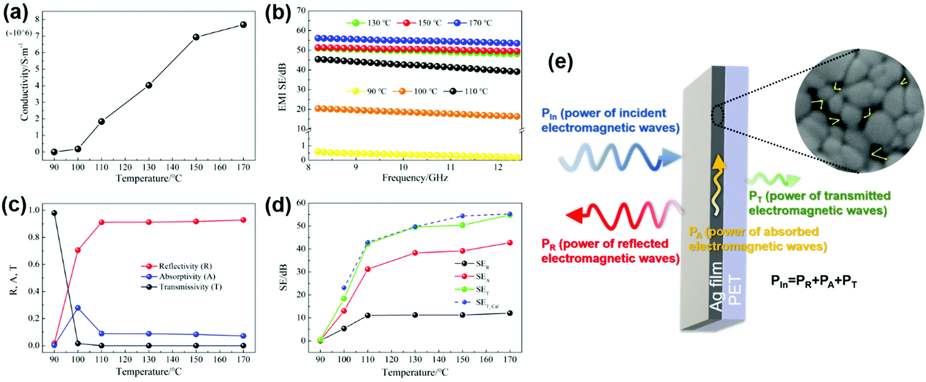 | ||
| Fig. 3 Properties of silver films thermally treated at different temperatures, (a) conductivities, (b) EMI SE in the X band, (c) power coefficients R, A, and T, (d) the comparison of SER, SEA, SET, and SET_Cal at 10.3 GHz, and (e) schematic EMI shielding mechanism of the nanoparticle silver film. | ||
Fig. 3b displays the EMI shielding effectiveness (SE) of the films cured at different temperatures measured in the frequency range of 8.2–12.4 GHz. As we can see, the electromagnetic shielding effectiveness of the film increases with the increase of curing temperature, which is similar to the changing trend of the conductivity. The film treated at 90 °C has an average effectiveness of only 0.45 dB mainly due to its poor conductivity, and the film treated at 100 °C shows a low conductivity of 2.02 × 10⁵ S m−1, hence, an average SE of 18.4 dB was observed. The films treated above 110 °C exhibited an outstanding EMI shielding performance, attributed to their ultra-high conductivity. The shielding effectiveness is slightly improved between 130 °C and 170 °C, reaching 49.68 dB at 130 °C and 55.25 dB at 170 °C, respectively. Similarly, with the increase of curing time, the conductivity increases from 1.73 × 10⁶ S m−1 to 4.81 × 10⁶ S m−1, and the corresponding electromagnetic shielding effectiveness increases from 42.93 dB to 50.94 dB, as shown in Fig. S3(d) and (f) (ESI†). The improvement of SE tends to be trivial, when the curing time is longer than 30 min. In consideration of the energy-saving synthesis of silver films with high shielding performance, the appropriate curing process is set as 130 °C for 30 min. The low curing temperatures make it possible that our ink can be applied to various flexible substrates. Many printing and coating technologies can be adopted for this ink to deposit the silver film or patterns, which makes the fabrication process easier and more economical. In this experiment, we select the spin coating method to fabricate more uniform films. By this fabrication method, the silver film possessed a high shielding effectiveness of 49.68 dB with a thickness of 400 nm.
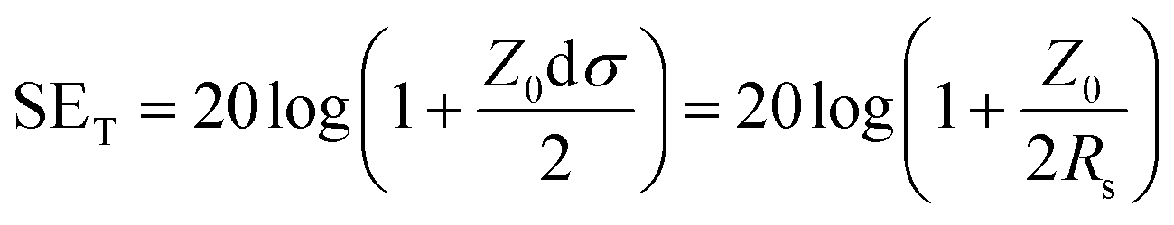
To clarify the outstanding EMI shielding performance of the ultra-thin silver films in this work, a theoretical analysis was carried out according to eqn (7) for electrically thin materials:37,38
 | (7) |
| δ = (πfμσ)−1/2 |
It is well known that shielding materials weaken the penetration ability of electromagnetic waves by means of reflection and absorption. The interaction mechanism between the incident electromagnetic wave and the shielding material is illustrated in Fig. 3e. The power coefficients R, A and T (shown as Fig. 3e) represent the ratio of the power of reflected, absorbed and transmitted electromagnetic waves to the incident electromagnetic waves, respectively, calculated from the S parameters using eqn (1)–(3). Fig. 3c shows the power coefficients R, A and T of silver films cured at different temperatures. R values are always greater than the corresponding A values, indicating that the incident electromagnetic waves on the silver film are mainly reflected off. This is determined by the nature of the shielding material itself due to the big impedance mismatch between silver and air.39 As we can see from Fig. 3e, the absorption of electromagnetic waves occurs after the surface reflection. Due to the large R value of silver films, most of the electromagnetic waves are reflected off and only a small part is incident with the silver film. Therefore, the reflection and absorption capability of silver films to electromagnetic waves cannot be judged according to the power coefficients.40 The EMI shielding effectiveness is used to characterize the ability of shielding materials to attenuate electromagnetic waves. The total SE (SET) is the sum of reflection shielding effectiveness (SER), absorption shielding effectiveness (SEA) and multiple reflection shielding effectiveness (SEM). As SEA is higher than 10 dB, SEM can be ignored.41,42 SER, SEA and SET are calculated from the power coefficient according to eqn (4)–(6). The contribution of SER and SEA to the total SE is usually used to elucidate the shielding mechanism.40,43,44 As observed in Fig. 3d, the average SER and SEA both increase initially with the increase of temperature. Although the values of SER become stable afterwards, the values of SEA always increase with the SET, indicating that SER contributes less than SEA. Furthermore, the value of SEA is always higher than the SER at any temperature. For example, the SER and SEA of the silver film heat treated at 130 °C for 30 min are 38.3 dB and 11.25 dB, accounting for 77% and 23% of the total SE (49.68 dB), respectively. Accordingly, the shielding mechanism of the silver films is mainly dominated by absorption. The network structure providing a large number of interfaces among the nanoparticles may be the reason for the absorption-dominated shielding mechanism. The incident electromagnetic waves are reflected and scattered in the pores formed among the nanoparticles, resulting in an effective absorption loss, as schematically shown in Fig. 3e.
3.2 Effects of the MOD silver ink concentration on the microstructures and properties of the films
Generally, the thickness of shielding materials will have an influence on their shielding performance.45–47 We adjust the film thickness by changing the ink concentrations and spin coating layers. To investigate the effects of the ink concentration, we synthesized four kinds of silver inks with different silver concentrations (0.25 M, 0.5 M, 1 M and 2 M). The corresponding films of the four inks are labeled as 0.25 M film, 0.5 M film, 1 M film and 2 M film, respectively. Fig. 4 shows the SEM images of silver films of different concentrations cured at 130 °C for 30 min. It can be seen that the surface morphology of these films was quite different. Films of low concentrations (0.25 M and 0.5 M) had a more uniform and smoother surface. On the other hand, the surfaces of films of high concentrations (1 M and 2 M) were not smooth. These films showed a microstructural feature of a “ridge” or “hill”-like morphology, which may be caused by the fast volatilization of the solvent during the curing process. With the increase of the silver concentration, the film roughness increases obviously from 0.017 μm to 0.971 μm. It should also be noted that the film thickness increases slightly from 200 nm to 500 nm.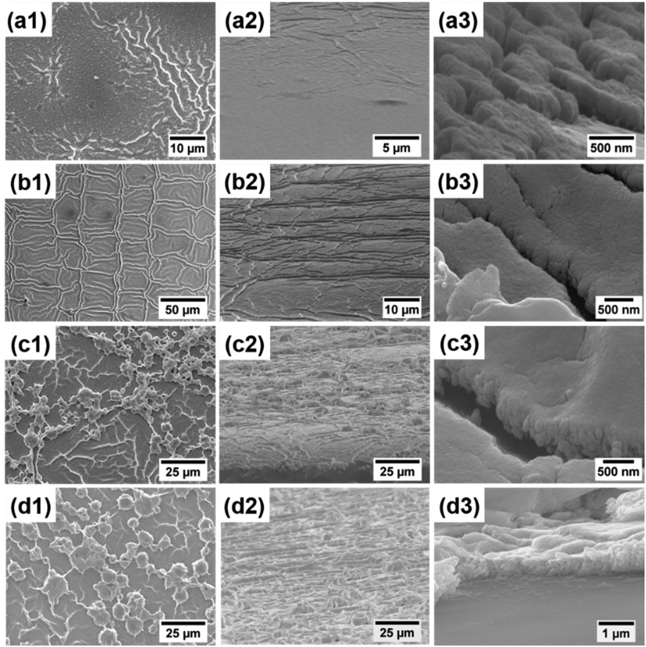 | ||
| Fig. 4 Surface (the left column) and cross-sectional (the middle and right columns) SEM images of films with different concentrations. (a1–a3) 0.25 M, (b1–b3) 0.5 M, (c1–c3) 1 M, and (d1–d3) 2 M. | ||
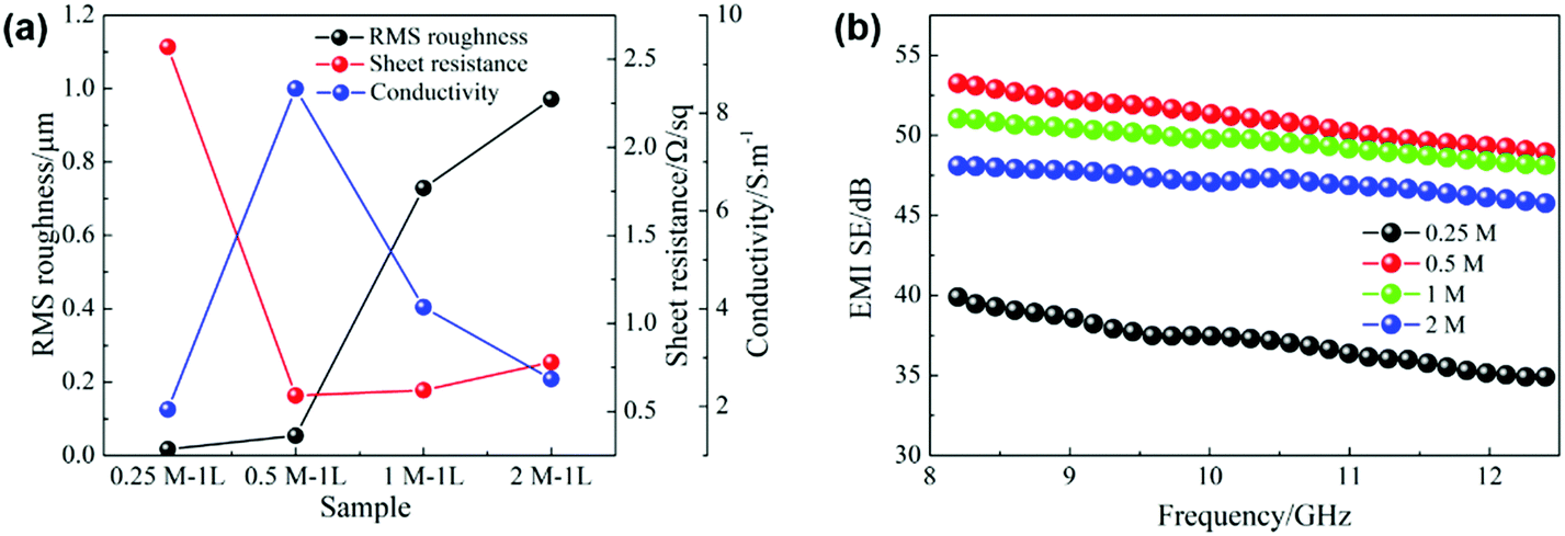
Fig. 5a displays the relationships between the sheet resistance, conductivity and roughness of silver films prepared with inks of different concentrations. Except for the 0.25 M film, with the increase of the ink concentration, the changing trend of sheet resistance is consistent with that of film roughness, ranging from 0.59 Ω sq−1 to 0.76 Ω sq−1, and the conductivity decreases greatly from 8.46 × 10⁶ S m−1 to 2.63 × 10⁶ S m−1. The low solid content of the 0.25 M ink results in nonsufficient nanoparticles to establish an efficient electrical network. Therefore, the 0.25 M film exhibits an inferior electrical performance, with 2.58 Ω sq−1 sheet resistance and 1.94 × 10⁶ S m−1 conductivity.
 | ||
| Fig. 5 (a) RMS roughness, sheet resistance and conductivity of films with different concentrations. (b) EMI SE in the X band. | ||
Fig. 5b shows the EMI shielding effectiveness (SE) of the films of different concentrations in the frequency range of 8.2–12.4 GHz. It can be seen that the electromagnetic shielding performances of silver films are mainly related to their electrical properties. In detail, the 0.25 M film with the worst electrical performance exhibits the lowest shielding performance. However, the 0.5 M film has the best conductivity and shielding effectiveness, with an average SE of up to 51.1 dB. Due to the decline of electrical properties affected by the large surface roughness, the shielding effectiveness of high concentration films (1 M, 2 M) decreases gradually. Accordingly, different ink concentrations cause the change of film surface roughness, and then affect their electrical properties and electromagnetic shielding performances.
3.3 Effects of spin coating layers on the microstructures and properties of the films
We spin coated several times to obtain multilayer films with different thicknesses. The four inks with different concentrations were used to prepare the corresponding single layer and multilayer films (three layers and six layers). The samples are marked as “concentration of the ink–number of layers”, for example, 0.25 M–1 L, 0.25 M–3 Ls and 0.25 M–6 Ls. The SEM images of silver films of 0.25 M, 0.5 M, 1 M and 2 M heat treated at 130 °C for 30 min with different layers are presented in Fig. 6. The surfaces of 0.25 M multilayer films are still smooth, and the film thickness increases from 200 nm for a single layer to 1.1 μm for six layers. However, there is an obvious difference in the morphology of the 0.5 M–1 L film and multilayer films. The increase of layers will disturb the regular and uniform morphology of the single layer film, and the surfaces of multilayer films are no longer smooth, with a more hill-shaped morphology. The thickness of 0.5 M films increases from 200 nm to 2.5 μm. The surface morphology of 1 M–1 L and 2 M–1 L is similar, with amounts of humps, resulting in high surface roughness. With the increase of layers, particles in subsequent layers will fill in the flat area of the previous film which no large particles occupy, which results in decreased roughness and improved uniformity. Moreover, there is a significant difference in the thickness between high concentration films with different layers. The thickness of 1 M films varies from 400 nm for a single layer to 7 μm for six layers, and that of 2 M films varies from 500 nm for a single layer to 7.5 μm for six layers. Therefore, the surface roughness and thickness of silver films with different layers and concentrations are quite different.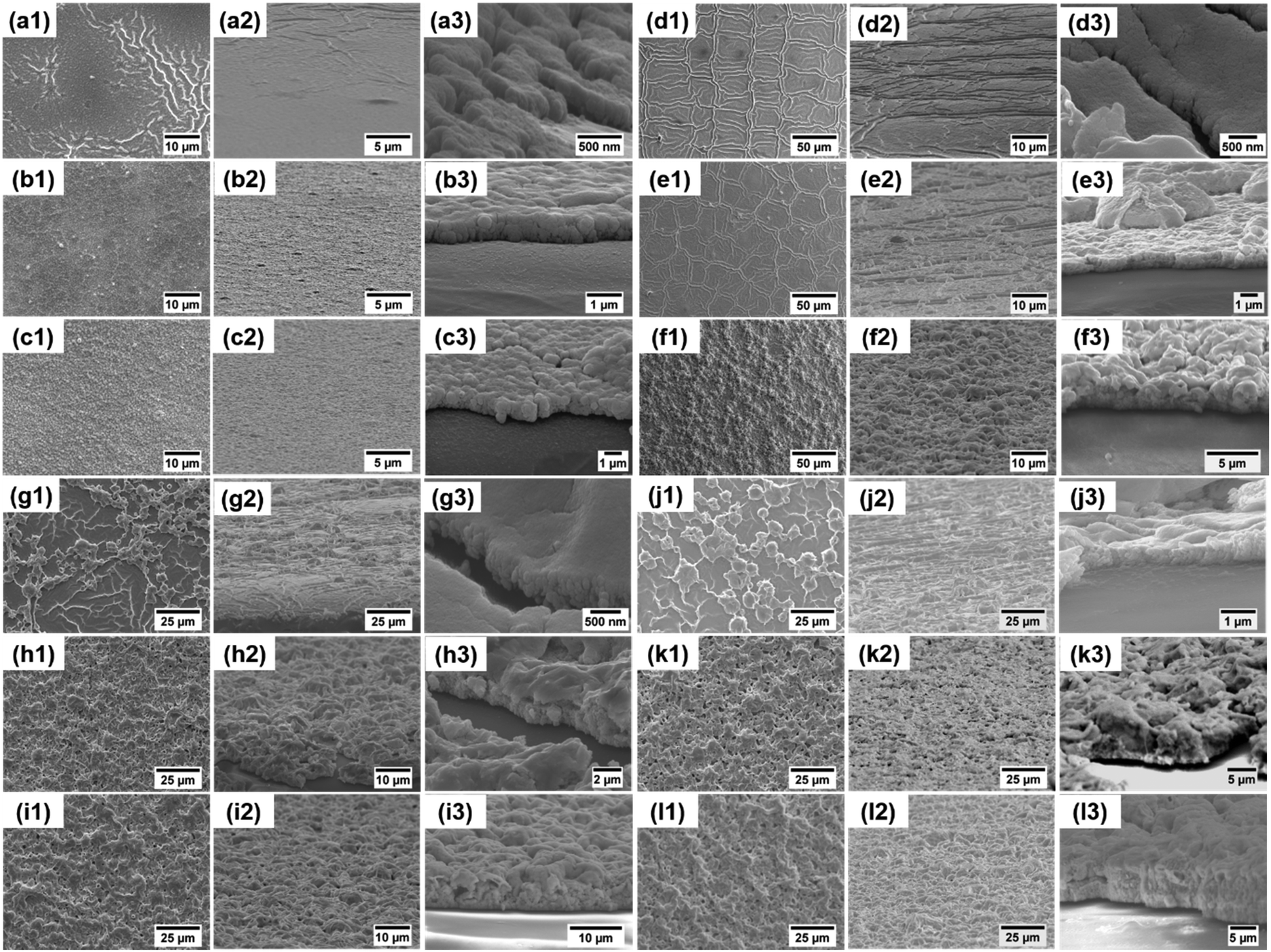 | ||
| Fig. 6 Surface and cross-sectional SEM images of silver films with different concentrations and layers. 0.25 M films with 1 layer (a1–a3), 3 layers (b1–b3), and 6 layers (c1–c3). 0.5 M films with 1 layer (d1–d3), 3 layers (e1–e3), and 6 layers (f1–f3). 1 M films with 1 layer (g1–g3), 3 layers (h1–h3), and 6 layers (i1–i3). 2 M films with 1 layer (j1–j3), 3 layers (k1–k3), and 6 layers (l1–l3). | ||
Then, we explore the relationship between surface roughness, sheet resistance and resistivity. According to the SEM images, due to the uniform morphology of 0.25 M films, the roughness can be detected by atomic force microscopy, as shown in Fig. 7a and Fig. S4 (ESI†). However, considering the uneven surfaces of other concentration films and the big variety of the roughness in different micro regions, a laser confocal microscope was used to observe the large area region (Fig. S5, ESI†) and obtain the average surface roughness, as shown in Fig. 7b–d. The changing trends of the roughness of low concentration films (0.25 M and 0.5 M) and high concentration films (1 M and 2 M) with layers are different. The roughness of low concentration films increases with layers, while that of high concentration films decreases, in good agreement with the above SEM observations. Fig. 7a–d also present the relationships between the sheet resistance, conductivity and roughness of silver films of 0.25 M, 0.5 M, 1 M and 2 M with different layers. It can be seen that, except for 0.25 M films, the changing trend of the sheet resistance of films with different layers is consistent with that of the roughness. With the increase of layers, the sheet resistance of 0.5 M films increases slightly from 0.59 Ω sq−1 to 0.77 Ω sq−1, and the sheet resistance of high concentration films decreases greatly. For high concentration films, the large shift of sheet resistance with layers is due to the significant change of thickness. As other studies reported, the sheet resistance of the film decreased with the increase of thickness.48 The abnormal changing trend of the roughness and sheet resistance of 0.25 M films between the single layer and three layers is mainly because of the insufficient silver nanoparticles of the 0.25 M–1 L film to establish an effective electrical transport network. Therefore, for the 0.25 M–3 Ls film, enough silver particles make the sheet resistance decrease significantly and the conductivity increase obviously. While for the 0.25 M–6 Ls film, the increase of surface roughness leads to the increase of sheet resistance. Therefore, it can be considered that the film roughness and a significant change of film thickness have an effect on the sheet resistance. For all the fabricated films, unlike the sheet resistance, the conductivity of films has no obvious changing trend with the layers and has no direct change relationship with the roughness.
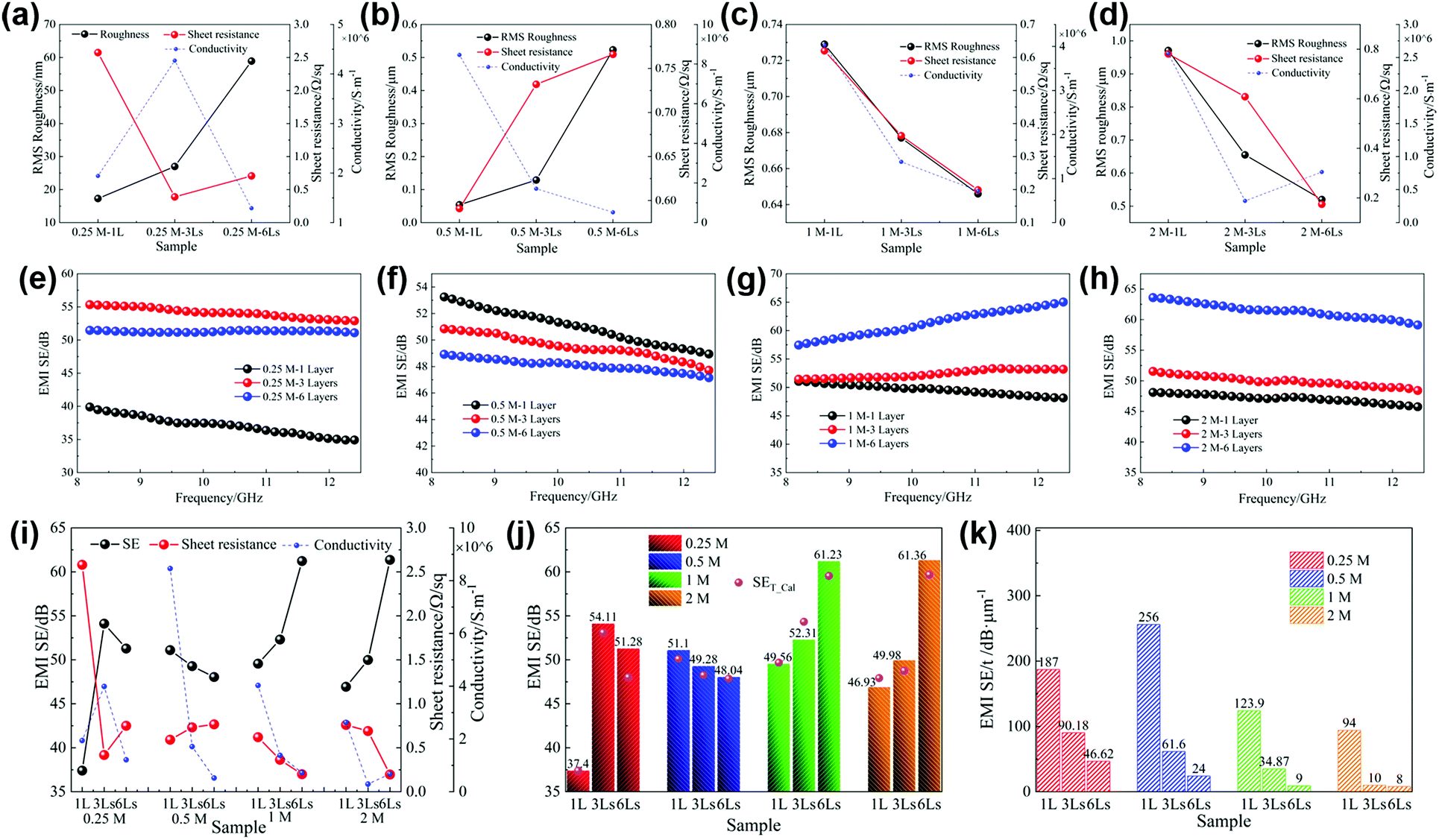 | ||
| Fig. 7 (a–d) RMS roughness, sheet resistance and conductivity of films with different layers, 0.25 M films (a), 0.5 M films (b), 1 M films (c), and 2 M films (d). (e–h) EMI SE of films with different layers in the X band, 0.25 M films (e), 0.5 M films (f), 1 M films (g), and 2 M films (h). (i) The relationship among the EMI SE, sheet resistance and conductivity of films with different layers and concentrations. (j) The average EMI SE and theoretical SE of all the above films. (k) Comparison of SE/t (the values of SE divided by sample thickness) among all the above films. | ||
The EMI shielding effectiveness of four concentration films with different layers in the X-band is shown in Fig. 7e–h and i displays the relationship between the shielding effectiveness, sheet resistance and conductivity of the above films. It can be found that the change of electromagnetic shielding effectiveness of all the fabricated films is only related to the sheet resistance, and the changing trend is opposite to that of the sheet resistance. We calculated their skin depths and found that for all films, the ratios of thickness to skin depth are all less than 1.3, indicating that eqn (7) can be used to calculate their theoretical SE. The average SE and theoretical SE of all the films are presented in Fig. 7j. It can be seen that there is little difference between the theoretical calculation values and the measured values, which not only demonstrates the reliability of the measured values, but also confirms that the shielding effectiveness of the conductive thin layer is directly related to the sheet resistance according to eqn (7). Furthermore, it is found that the measured values of most films are slightly larger than the theoretical values, which may be due to the network structure of nanoparticles. The incident electromagnetic waves can be reflected multiple times in the porosity among the nanoparticles of the silver film, which increases the energy loss of electromagnetic waves. Moreover, the increase of multilayer film thickness and the introduction of pores between interlayers will also make the transmission path of incident electromagnetic waves become longer and the multiple reflected loss will be enhanced, which will further improve the electromagnetic shielding effectiveness.
From the above analysis, it can be concluded that the shielding effectiveness of silver films fabricated by this method is related to sheet resistance. Multilayers will affect the roughness and thickness of films, which will further affect the sheet resistance and the shielding effectiveness. For low concentration films (0.5 M), increasing the layers has an adverse effect on the shielding performance by increasing the film roughness. However, for high concentration films, multilayer films (1 M, 2 M) show better shielding performance, attributed to the lower roughness and larger thickness. Therefore, among all the fabricated films, the 2 M–6 Ls film exhibits the best shielding performance, with an average SE of 61.36 dB. Besides the high conductivity, the ultrathin thickness is another advantage of this method. Considering this, the values of SE divided by sample thickness, SE/t, are presented in Fig. 7k. The SE/t of single layer films with any concentration is larger than that of their corresponding multilayer films. Among them, the 0.5 M–1 L film has the largest SE/t, up to 256 dB μm−1. In comparison with other studies related to silver coatings or films (Table 1), this work has the best SE/t, highlighting the ultrathin characteristic and high shielding performance of this silver film prepared from the silver MOD ink. Furthermore, the silver films in this work have better flexible reliability. After multiple bending tests, the electromagnetic shielding effectiveness of the silver films is still above 50 dB (Fig. S6, ESI†), demonstrating that the silver films can be well applied in flexible wearable devices.
| Sample | Fabrication method | Frequency/GHz | Conductivity/S m−1 | Thickness/μm | SE/dB | SE/t/dB μm−1 |
|---|---|---|---|---|---|---|
| AgNPs/PLA microfibers49 | Electroless deposition | 8.2–12.4 | 254 | 1500 | 50 | 0.033 |
| AgNPs@CFs nonwoven fabrics50 | Electroless deposition | 8.2–12.4 | 3.3 × 10⁴ | 500 | 111 | 0.222 |
| PP/PDA/AgNPs/PDMS51 | Chemical reduction | 8.2–12.4 | 8.12 × 10³ | 350 | 71.2 | 0.2 |
| CNFs@PDA@AgNPs composite films52 | Electroless deposition | 8.2–12.4 | 1 × 10⁶ | 167.2 | 93.8 | 0.56 |
| AgNW/cellulose38 | Dip-coating | 1 | 6.75 × 10³ | 160 | 48.6 | 0.3 |
| PAN@SiO2–Ag-PFDT film53 | Electroless deposition | 8.2–12.4 | 1.78 × 10⁴ | 50 | 81.01 | 1.62 |
| Ag/WPU coating18 | Silver flakes ink | 8.2–12.4 | 1.43 × 10⁶ | 10 | 73.6 | 7.36 |
| Ag film54 | Atmospheric pressure plasma reduction | 0.1 | 4.41 × 10⁶ | 0.93 | 60.49 | 65 |
| Ag film55 | Spray coating | 1–1.5 | 1.2 × 10⁶ | 0.2 | 45 | 225 |
| 0.5 M–1 L Ag film (this work) | Silver MOD ink | 8.2–12.4 | 8.46 × 10⁶ | 0.2 | 51.1 | 256 |
4. Conclusion
In this study, flexible silver films with ultrathin thickness and high shielding performance were fabricated from the silver oxalate-1,2-diaminopropane ink. The efficient electron transport network structure of films constructed by interconnected silver nanoparticles brings about ultrahigh conductivity and excellent shielding effectiveness. A large number of interfaces among the nanoparticles helps in determining the absorption dominated shielding mechanism of silver films. The thermal treatment process has influences on the decomposition degree of the silver amine complex and the microstructure of films, and then affects the conductivity and shielding effectiveness. A suitable thermal treatment for the silver oxalate-1,2-diaminopropane ink is at 130 °C for 30 min. The electromagnetic shielding performance of silver films by this method is determined by sheet resistance, which is influenced by the roughness and thickness of films. By adjusting the ink concentrations and film layers, the obtained films are with a large range of roughness and thickness, resulting in different shielding performances. Considering the ultrathin characterization, the single layer film prepared from the 0.5 M ink was the best film, with a high EMI shielding effectiveness of 51.1 dB and just only a 200 nm thickness. Consequently, the silver MOD ink is promising to be applied in industrial production for EMI shielding films.Conflicts of interest
There are no conflicts to declare.Acknowledgements
This work was supported by the National Key R&D Program of China (No. 2017YFB0305700), the National Natural Science Foundation of China (No. 52072063) and the China Academy of Engineering Physics (NSAF) (No. U1630137).References
- D. Wanasinghe and F. Aslani, Composites, Part B, 2019, 176, 107207 CrossRef CAS.
- Y. N. Gao, Y. Wang, T. N. Yue, B. Zhao, R. Che and M. Wang, Chem. Eng. J., 2022, 430, 132949 CrossRef CAS.
- H. Liu, S. Wu, C. You, N. Tian, Y. Li and N. Chopra, Carbon, 2021, 172, 569–596 CrossRef CAS.
- X. H. Tang, Y. Tang, Y. Wang, Y. X. Weng and M. Wang, Composites, Part A, 2020, 139(10), 106116 CrossRef CAS.
- Y. Zhang, Z. Yang, T. Pan, H. Gao, H. Guan, J. Xu and Z. Zhang, Composites, Part A, 2020, 137, 105994 CrossRef CAS.
- M. Wang, X. H. Tang, J. H. Cai, H. Wu, J. B. Shen and S. Y. Guo, Carbon, 2021, 177, 377–402 CrossRef CAS.
- A. Iqbal, P. Sambyal and C. M. Koo, Adv. Funct. Mater., 2020, 30, 2000883 CrossRef CAS.
- P. Kumar, Adv. Mater. Interfaces, 2019, 6, 1901454 CrossRef.
- Y. Cheng, H. Zhao, H. Lv, T. Shi, G. Ji and Y. Hou, Adv. Electron. Mater., 2020, 6, 1900796 CrossRef CAS.
- O. Pitkanen, J. Tolvanen, I. Szenti, A. Kukovecz, J. Hannu, H. Jantunen and K. Kordas, ACS Appl. Mater. Interfaces, 2019, 11, 19331–19338 CrossRef CAS.
- B. Shen, W. Zhai and W. Zheng, Adv. Funct. Mater., 2014, 24, 4542–4548 CrossRef CAS.
- L. Kuo-Hsien, A. C. H. Chan, S. C. Hsien, I. C. Lin and H. H. Wen, 2012 2nd Ieee Cpmt Symposium Japan, Ieee, New York, 2012.
- S. Erickson and M. Sakaguchi, 2020 Ieee 70th Electronic Components and Technology Conference, Ieee Computer Soc, Los Alamitos, 2020, pp. 1691–1696 DOI:10.1109/ectc32862.2020.00265.
- K. Mukai, B. Eastep, K. Kim, L. Gaherty, A. Kashyap and I. C. Soc, 2016 Ieee 66th Electronic Components and Technology Conference, Ieee Computer Soc, Los Alamitos, 2016, pp. 1530–1537 DOI:10.1109/ectc.2016.375.
- M. F. Tai, S. L. Kok and K. Mukai, and Ieee, in 2016 Ieee 37th International Electronics Manufacturing Technology, Ieee, New York, 2016.
- M. F. Tai, S. L. Kok and K. Mukai, 2016 Ieee 37th International Electronics Manufacturing Technology, Ieee, New York, 2016.
- X. Hong, Q. Z. Zhuo, X. P. Cao, D. Maslyk, N. Ekstrom, J. Sanchez, S. Hernandez and J. Choi, 2019 Ieee 69th Electronic Components and Technology Conference, Ieee, New York, 2019, pp. 753–757 DOI:10.1109/ectc.2019.00119.
- L. C. Jia, C. G. Zhou, W. J. Sun, L. Xu, D. X. Yan and Z. M. Li, Chem. Eng. J., 2020, 384, 123368 CrossRef CAS.
- Q. J. Huang and Y. Zhu, Adv. Mater. Technol., 2019, 4, 1800546 CrossRef.
- C. Cano-Raya, Z. Z. Denchev, S. F. Cruz and J. C. Viana, Appl. Mater. Today, 2019, 15, 416–430 CrossRef.
- Y. Choi, K. D. Seong and Y. Piao, Adv. Mater. Interfaces, 2019, 6, 1901002 CrossRef CAS.
- L. C. Zhuo, W. Liu, Z. Zhao, E. H. Yin, C. Li, L. Zhou, Q. Q. Zhang, Y. Y. Feng and S. Lin, Chem. Phys. Lett., 2020, 757, 137904 CrossRef CAS.
- B. Y. Ahn and J. A. Lewis, Mater. Chem. Phys., 2014, 148, 686–691 CrossRef CAS.
- Y. Dong, X. D. Li, S. H. Liu, Q. Zhu, J. G. Li and X. D. Sun, Thin Solid Films, 2015, 589, 381–387 CrossRef CAS.
- Y. Dong, X. D. Li, S. H. Liu, Q. Zhu, M. Zhang, J. G. Li and X. D. Sun, Thin Solid Films, 2016, 616, 635–642 CrossRef CAS.
- J. P. Fernandez-Blazquez, D. Fell, E. Bonaccurso and A. del Campo, J. Colloid Interface Sci., 2011, 357, 234–238 CrossRef CAS PubMed.
- Y. Yang, C. P. Feng, Y. C. Zhou, X. J. Zha, R. Y. Bao, K. Ke, M. B. Yang, C. B. Tan and W. Yang, Composites, Part A, 2020, 136, 105967 CrossRef CAS.
- W. J. Yuan, J. Z. Yang, F. X. Yin, Y. B. Li and Y. Ye, Compos. Commun., 2020, 19, 90–98 CrossRef.
- A. L. Dearden, P. J. Smith, D. Y. Shin, N. Reis, B. Derby and P. O'Brien, Macromol. Rapid Commun., 2005, 26, 315–318 CrossRef CAS.
- Y. Mou, H. Cheng, H. Wang, Q. L. Sun, J. X. Liu, Y. Peng and M. X. Chen, Appl. Surf. Sci., 2019, 475, 75–82 CrossRef CAS.
- Y. G. Cai, X. J. Yao, X. Q. Piao, Z. J. Zhang, E. Nie and Z. Sun, Chem. Phys. Lett., 2019, 737, 136857 CrossRef CAS.
- X. L. Nie, H. Wang and J. Zou, Appl. Surf. Sci., 2012, 261, 554–560 CrossRef CAS.
- K. S. Bhat, R. Ahmad, Y. Wang and Y. B. Hahn, J. Mater. Chem. C, 2016, 4, 8522–8527 RSC.
- Y. Dong, Z. J. Lin, X. D. Li, Q. Zhu, J. G. Li and X. D. Sun, J. Mater. Chem. C, 2018, 6, 6406–6415 RSC.
- M. Vaseem, G. McKerricher and A. Shamim, ACS Appl. Mater. Interfaces, 2016, 8, 177–186 CrossRef CAS PubMed.
- W. Xu, X. F. Dai, T. Zhang and T. Wang, Chem. Eng. Sci., 2018, 190, 40–47 CrossRef CAS.
- C. S. Zhang, Q. Q. Ni, S. Y. Fu and K. Kurashiki, Compos. Sci. Technol., 2007, 67, 2973–2980 CrossRef CAS.
- T. W. Lee, S. E. Lee and Y. G. Jeong, ACS Appl. Mater. Interfaces, 2016, 8, 13123–13132 CrossRef CAS PubMed.
- K. Rajavel, Y. G. Hu, P. L. Zhu, R. Sun and C. P. Wong, Chem. Eng. J., 2020, 399, 125791 CrossRef CAS.
- G. Yin, Y. Wang, W. Wang and D. Yu, Colloids Surf., A, 2020, 601, 108071 CrossRef.
- T. K. Gupta, B. P. Singh, S. R. Dhakate, V. N. Singh and R. B. Mathur, J. Mater. Chem. A, 2013, 1, 9138–9149 RSC.
- P. Saini, V. Choudhary, B. P. Singh, R. B. Mathur and S. K. Dhawan, Synth. Met., 2011, 161, 1522–1526 CrossRef CAS.
- Y. Chen, P. Potschke, J. Pionteck, B. Voit and H. S. Qi, ACS Appl. Mater. Interfaces, 2020, 12, 22088–22098 CrossRef CAS.
- T. Wang, W. C. Yu, C. G. Zhou, W. J. Sun, Y. P. Zhang, L. C. Jia, J. F. Gao, K. Dai, D. X. Yan and Z. M. Li, Composites, Part B, 2020, 193, 108015 CrossRef CAS.
- Q. W. Wei, S. F. Pei, X. T. Qian, H. P. Liu, Z. B. Liu, W. M. Zhang, T. Y. Zhou, Z. C. Zhang, X. F. Zhang, H. M. Cheng and W. C. Ren, Adv. Mater., 2020, 32, 1907411 CrossRef CAS.
- F. Liu, Y. C. Li, S. Hao, Y. Cheng, Y. H. Zhan, C. M. Zhang, Y. Y. Meng, Q. Xie and H. S. Xia, Carbohydr. Polym., 2020, 243, 116467 CrossRef CAS PubMed.
- S. Mondal, R. Ravindren, P. Bhawal, B. Shin, S. Ganguly, C. Nah and N. C. Das, Composites, Part B, 2020, 197(15), 108071 CrossRef CAS.
- X. M. Fang, T. L. Ma, G. Q. Guan, M. Akiyama, T. Kida and E. Abe, J. Electroanal. Chem., 2004, 570, 257–263 CrossRef CAS.
- K. Zhang, H.-O. Yu, K.-X. Yu, Y. Gao, M. Wang, J. Li and S. Guo, Compos. Sci. Technol., 2018, 156, 136–143 CrossRef CAS.
- Y. J. Tan, J. Li, Y. Gao, J. Li, S. Y. Guo and M. Wang, Appl. Surf. Sci., 2018, 458, 236–244 CrossRef CAS.
- J. C. Luo, L. Wang, X. W. Huang, B. Li, Z. Guo, X. Song, L. W. Lin, L. C. Tang, H. G. Xue and J. F. Gao, ACS Appl. Mater. Interfaces, 2019, 11, 10883–10894 CrossRef CAS PubMed.
- Y. F. Xu, K. P. Qian, D. M. Deng, L. Q. Luo, J. H. Ye, H. M. Wu, M. Miao and X. Feng, Carbohydr. Polym., 2020, 250, 116915 CrossRef CAS.
- T. T. Li, Y. T. Wang, H. K. Peng, X. F. Zhang, B. C. Shiu, J. H. Lin and C. W. Lou, Composites, Part A, 2020, 128, 105685 CrossRef CAS.
- H. J. Oh, V. D. Dao and H. S. Choi, Appl. Surf. Sci., 2018, 435, 7–15 CrossRef CAS.
- D. X. Chen, Z. X. Kang and W. Li, J. Appl. Polym. Sci., 2021, 138, 49806 CrossRef CAS.
Footnote |
| † Electronic supplementary information (ESI) available. See DOI: 10.1039/d1ma00918d |
| This journal is © The Royal Society of Chemistry 2022 |