DOI:
10.1039/D1MA00862E
(Paper)
Mater. Adv., 2022,
3, 1587-1593
Perpendicular-spin-transfer-torque magnetic-tunnel-junction neuron for spiking neural networks depending on the nanoscale grain size of the MgO tunnelling barrier†
Received
18th September 2021
, Accepted 23rd December 2021
First published on 24th December 2021
Abstract
Unlike conventional neuromorphic chips fabricated with C-MOSFETs and capacitors, those utilizing p-STT MTJ neuron devices can achieve fast switching (on the order of several tens of nanoseconds) and extremely low power consumption (<0.2 pJ per spike). A p-STT MTJ neuron with a sensing circuit, which is composed of one p-STT MTJ neuron device, seven n-MOSFETs, three p-MOSFETs, and one reference resistor, was constructed in this study and presented integrate-and-fire characteristics for use in spiking neural networks. In particular, the difference in resistance between the no-spiking input and after the implementation of integration-and-fire was found to be principally determined by the average nanoscale grain size (i.e., 0.418 to 1.141 nm) and face-centered-cubic crystallinity of the MgO tunnelling barrier of the p-STT MTJ neuron devices. Therefore, a larger grain size and better crystallinity led to a larger resistance difference in these devices. MNIST pattern recognition tests (achieving a testing accuracy of 90.34%) using the p-STT MTJ neurons were conducted for demonstrating a spiking neural network.
Introduction
Current neuromorphic chips have been developed based on conventional C-MOSFET-based integrated circuits. However, this presents a challenge for achieving a high neuronal density owing to the large area of the capacitor of the C-MOSFET with a feature size of approximately 1000 F2.1,2 Power consumption is another issue owing to the leakage current of these MOSFETs. There have been significant research efforts to replace C-MOS-implemented neuromorphic chips with emerging memory devices to overcome this issue.3–12 Particularly, spin-electron-based devices have been proposed as a promising candidate due to their fast operation speed (on the order of several ns) and low power consumption (∼0.1 pJ per spike).13,14 Domain-wall-movement-based spin electron devices, which are fabricated with a structure of 3-electrodes, have been theoretically proposed by K. Roy et al. However, they are not suitable for high-density integration because of their 3-electrode structure.15–18 As a practical spin-neuron device, stochastic perpendicular-spin-transfer-torque magnetic-tunnelling-junction (p-STT MTJ) neuron devices with 2-electrode structures have been reported, but they are limited to stochastic computing because their use of switching probability.19–22 Therefore, in their application towards deterministic neural networks, p-STT MTJ neuron devices have demonstrated an integration-and-fire behaviour rather than stochastic behaviour, indicating their potential use in spiking neural networks (SNNs).23
p-STT MTJ neuron devices with integration behaviour operate in an integrate-and-fire manner when the resistance of the p-STT MTJ neuron device reaches a certain threshold resistance via the integrated input spikes. The mechanism of the integration behaviour could be explained by the switching energy difference depending on the grain size of the MgO tunnelling barrier inside of the p-STT MTJ neuron device.24 In addition, it has been reported that the nanoscale grain size and face-centered-cubic (f.c.c.) crystallinity of the MgO tunnelling barrier were principally determined by the sputtering process parameters of the MgO tunnelling barrier, such as the radio-frequency (RF) sputtering power and ambient gas conditions.25 Therefore, a precise nanoscale grain size design in the MgO tunnelling barrier is essential for the fabrication of p-STT MTJ neuron devices with integrate behaviour, which could be tested using a 12-inch-wafer ultra-high-vacuum (i.e., 10−9 Pa) multi-chamber cluster magnetron-sputter system. In this study, the nanoscale grain size of an MgO tunnelling barrier for a p-STT MTJ neuron device is accurately designed by varying the RF sputtering power of the MgO tunnelling barrier using the same thickness of the MgO tunnelling barrier for all devices. In particular, the nanoscale grain size and the f.c.c. crystallinity of the MgO tunnelling barrier are characterized using high-resolution transmission electron microscopy (HR-TEM). In addition, the integrate behaviour of the p-STT MTJ neuron devices is investigated as a function of the nanoscale grain size distribution. Finally, a neuron circuit using the fabricated p-STT MTJ neuron device is designed and simulated for a SNN operation, such as Modified National Institute of Standards and Technology database (MNIST) pattern recognition.
Results and discussion
Results and discussion Electrical properties of p-STT MTJ neuron devices
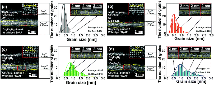
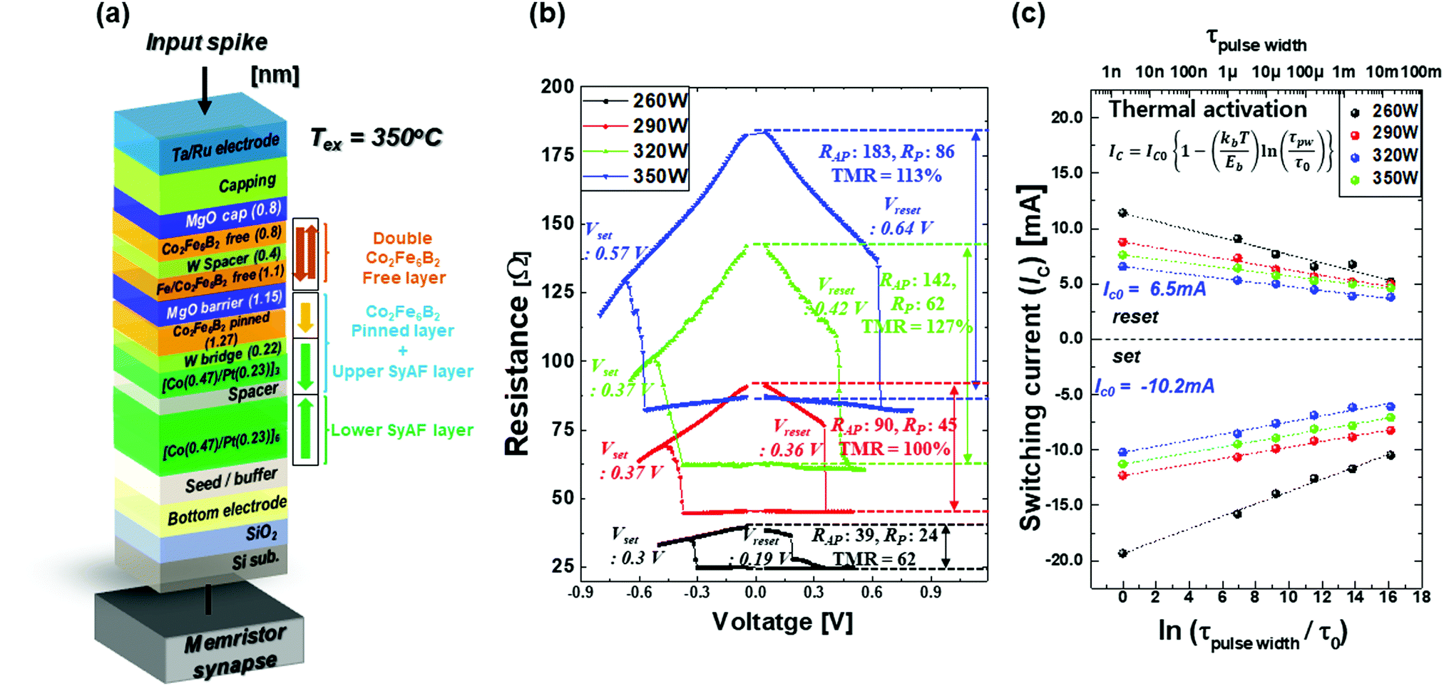
First, the static magnetization behaviours of the p-STT MTJ neuron devices in Fig. 1a were investigated to confirm whether they contain the interfacial-perpendicular-magnetic-anisotropy (i-PMA) characteristic (i.e., squareness), as shown in Fig. S1 (ESI†). The static magnetization behaviours of the p-STT MTJ neuron devices were not affected by the MgO sputtering power because the i-PMA characteristics of the p-STT MTJs were independent of the MgO sputtering power, as shown in the insets of Fig. S1 (ESI†). Note that the thickness of the MgO tunnelling barrier was fixed at 1.15 nm for all sputtering conditions. This result indicates that the M–H curve is not dependent on the crystallinity of the MgO tunnelling barrier.25,26 However, the electrical properties of the MgO tunnelling barrier, as determined by the tunnelling probability of the spin electrons and sputtering power, can be influenced by the f.c.c. crystallinity and grain size distribution of the MgO tunnelling barrier (although the M–H curves of the MgO tunnelling barrier were independent of the MgO sputtering power). To clarify the dependencies of the electrical properties of this system on the MgO sputtering power, the resistance versus voltage (R–V) curves of the p-STT MTJ neuron device with a 1.6 μm device diameter were obtained as a function of the MgO sputtering power, as shown in Fig. 1b. The set and reset voltages increased from 0.3 to 0.57 V and 0.19 to 0.64 V, respectively, and the parallel resistance increased from 24 to 86 Ω as the MgO sputtering power increased from 260 to 350 W. Moreover, the tunnelling magneto-resistance (TMR) ratio of the p-STT MTJ neuron device increased from 62% to 127% as the MgO sputtering power increased from 260 to 320 W, and it then decreased to 113% when the MgO sputtering power was further increased to 350 W. The TMR ratio (i.e., 127%) peaked at an MgO sputtering power of 320 W. This dependency of the TMR ratio on the MgO sputtering power for p-STT MTJ neuron devices was confirmed by the dependency of the TMR ratio on the MgO sputtering power for non-patterned 12-inch p-MTJ wafers measured by Current-In-Plane Tunnelling (CIPT) measurement, where the TMR ratio (170%) peaked at 320 W, as shown in Fig. S2 (ESI†). This dependency of the TMR ratio on the MgO sputtering power for p-STT MTJ neuron devices is related to the dependency of the surface roughness of the MgO tunnelling barrier on the ferromagnetic Co2Fe6B2 pinned layer, as well as the dependencies of the grain size distribution and f.c.c. crystallinity of the MgO tunnelling barrier. It should be noted that a higher MgO sputtering power leads to better f.c.c. crystallinity, a large grain size and distribution, and a higher surface roughness of the MgO tunnelling barrier, as shown in Fig. 2, Fig. S3, and S4 (ESI†). In addition, a better f.c.c. crystallinity, smaller grain size distribution, and lower surface roughness of the MgO tunnelling barrier resulted in a higher TMR ratio of the p-STT MTJ.25–35 As a result, the TMR ratio (127%) of the p-STT MTJ neuron devices peaked at a specific MgO sputtering power of 320 W. The switching current,  , of the p-STT MTJ neuron devices depending on the MgO sputtering power was measured using different pulse widths (1 μs, 10 μs, 100 μs, 1 ms, and 10 ms), where Ic is the threshold current, Ic0 is the switching threshold current at 0 K, Eb is the switching energy barrier between the P and AP states, τpw is the pulse width, and τ0 (i.e., 1 ns) is the attempt time, as shown in Fig. 1c. The switching currents for reset (i.e., 6.5 mA) and set (i.e., −10.2 mA) conditions were the lowest at 320 W, which is associated with the dependencies of the f.c.c. crystallinity, grain size and distribution, and surface roughness of the MgO tunnelling barrier sputtering-power.36–38 The current flowing through the MTJ can be divided by two different currents. One is the coherent tunnelling current of the MTJ inside the MgO grain, and the other is the leakage current through the grain boundary. At smaller grain sizes with average of 0.418 nm, the leakage current would take a larger proportion of the current, so it requires more current to switch the CoFeB free layer. As the grain size increases to 0.935 nm, the overall grain boundary area decreases which would increase the proportion of the tunnelling current, so the switching current was reduced. At larger grain size with average of 1.141 nm (i.e., 350 W), the switching current was increased because the coherent tunnelling was reduced as the roughness increased with the MgO sputtering power which reduces the interfacial PMA. Generally, a higher resistance difference (i.e., the difference between the antiparallel and parallel resistances) and lower switching current result in better integrate characteristics for p-STT MTJ neuron devices.23 Therefore, the dependencies of the TMR ratio and switching current on the sputtering power would directly affect the integrate behaviour of p-STT MTJ neuron devices because the MgO sputtering power principally influences the f.c.c. crystallinity and grain size distribution.25
 |
| | Fig. 1 Dependency of electrical properties on MgO tunneling barrier sputtering power for p-STT MTJ neuron device. (a) a schematic structure of p-STT MTJ neuron device, (b) R–V curve of p-STT MTJ neuron device depending on MgO RF sputtering power, and (c) switching current of p-MTJ neuron device depending on MgO RF sputtering power. | |
 |
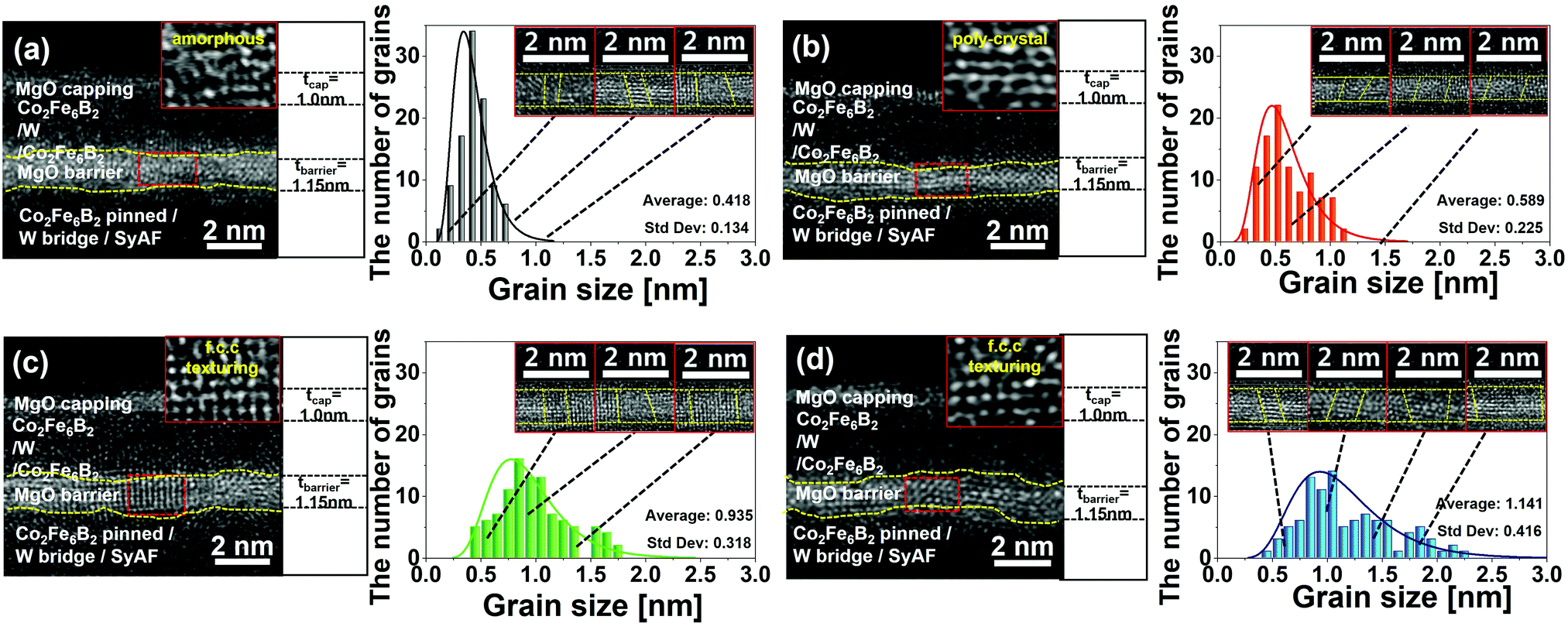
| | Fig. 2 Dependency of crystallinity and average grain size distribution on the RF sputtering power for MgO tunneling barrier. The thickness of MgO tunneling barrier was fixed with 1.15 nm for all p-STT MTJ neuron device. xHR-TEM images of the MgO tunneling barrier of p-STT MTJ neuron devices RF-sputtered at (a) 260, (b) 290, (c) 320, and (d) 350 W. | |
Dependence of the nanoscale grain size and f.c.c. crystallinity of the MgO tunnelling barrier on the sputtering power
To investigate how the MgO sputtering power influences the f.c.c. crystallinity and grain size distribution of the MgO tunnelling barrier, HR-TEM images of the p-STT MTJ neuron devices were obtained as a function of the MgO sputtering power, as shown in Fig. 2. Here, the MgO tunnelling barrier thickness was fixed at 1.15 nm for all p-STT MTJ neuron devices. At MgO sputtering power of 260 W, the MgO tunnelling barrier showed a mixture of amorphous and f.c.c. crystallized grains because the sputtering power is not sufficient to form a fully crystallized MgO tunnelling barrier, as shown in the cross-sectional (x) HR-TEM image in Fig. 2a. The average grain size was 0.418 nm, and its standard deviation was 0.134 nm with a sharp distribution, as shown on the right-hand side of Fig. 2a. At 290 W, the MgO tunnelling barrier exhibited a nearly f.c.c. polycrystalline phase, as shown in the x-HRTEM image in Fig. 2b, and the average grain size was 0.589 nm with a standard deviation of 0.225 nm, as shown on the right-hand side of Fig. 2b. At 320 W, the MgO tunnelling barrier presented a fully f.c.c. polycrystalline phase, as shown in the x-HRTEM image in Fig. 2c, and the average grain size was 0.935 nm with a standard deviation of 0.318 nm, as shown on the right-hand side of Fig. 2c. At 350 W, the MgO tunnelling barrier also demonstrated a fully f.c.c. polycrystalline phase, as shown in the x-HRTEM image in Fig. 2d, and the average grain size was 1.141 nm with a standard deviation of 0.416 nm, as shown on the right-hand side of Fig. 2d. These results indicate that the average grain size and standard deviation of the MgO tunnelling barrier increased with the MgO sputtering power. In particular, the grain size increased from 0.418 to 1.141 nm and the standard deviation increased from 0.134 to 0.416 nm when the MgO sputtering power increased from 260 to 350 W.38–40
Integrate-and-fire behaviour of p-STT MTJ neurons with a sensing circuit
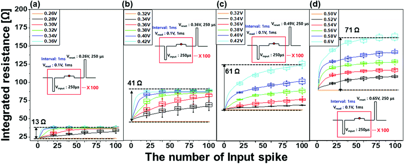
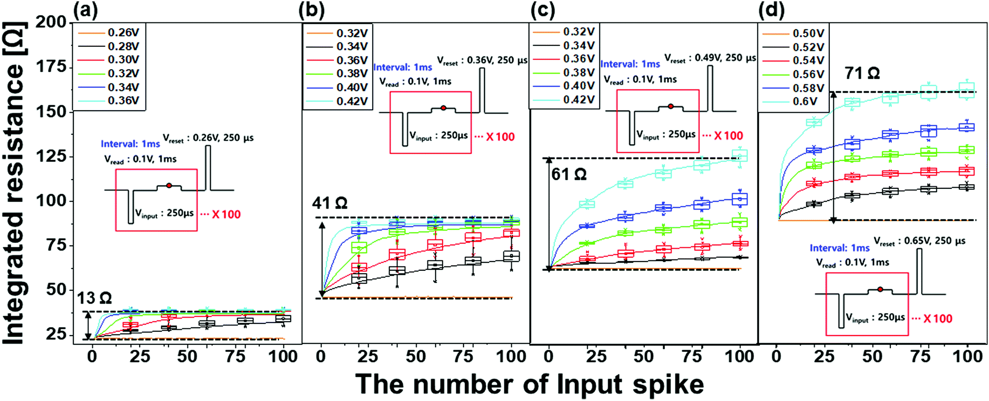
To better understand the mechanism underlying the influence of the grain size distribution of the MgO tunnelling barrier of p-STT MTJ neuron devices on the integrate behaviour of these devices, the dependency of the integrate characteristics on the grain size distribution of the MgO tunnelling barrier was estimated. This estimation was achieved by measuring the resistance versus the number of input spikes as a function of the spike amplitude, where the spike width was 250 μs, 100 spike were input, the read pulse amplitude and width were 0.1 V and 1 ms, respectively, and the read pulses were input between the input spikes, as shown in Fig. 3. Fundamentally, the resistance of the p-STT MTJ neuron device changes from a parallel to an antiparallel state between the double Co2Fe6B2 free layer and the Co2Fe6B2 pinned layer (see Fig. 1a) when the number of input spikes increases. It should be noted that the input spike amplitude should be much less than the spike amplitude, resulting in complete switching from the parallel to the anti-parallel state. The integrate behaviour was estimated using 10 repetitions to investigate the variation of the integrate behaviour, where a reset pulse with a 250 μs width was applied to every 100 input spikes. First, considering the p-STT MTJ neuron device with an average grain size and standard deviation of 0.418 and 0.134 nm, respectively, in the MgO tunnelling barrier, the spike amplitude was varied from 0.26 to 0.36 V with a reset spike amplitude of 0.26 V. It was observed that the resistance increased with the number of input spikes, which is referred to as an integrate behaviour, except at a spike amplitude of 0.26 V, as shown in Fig. 3a. In particular, for a maximum input spike amplitude (i.e., 0.36 V), the maximum resistance difference was 13 Ω, which would be insufficient to achieve sensing at a neuron with a sensing circuit. Second, for the p-STT MTJ neuron device with average grain size and standard deviation of 0.589 and 0.225 nm, respectively, in the MgO tunnelling barrier, the spike amplitude was varied from 0.32 to 0.42 V with a reset spike amplitude of 0.36 V. The resistance of this system also increased with the number of input spikes for all spike amplitudes except 0.32 V, as shown in Fig. 3b. In particular, for a maximum input spike amplitude (i.e., 0.42 V), the maximum resistance difference between having 0 and 100 input spikes was 41 Ω, which indicates the possibility of achieving sensing at a neuron with a sensing circuit. Third, considering the p-STT MTJ neuron device with an average grain size and standard deviation of 0.935 and 0.318 nm, respectively, in the MgO tunnelling barrier, the spike amplitude was varied from 0.32 to 0.42 V with a reset spike amplitude of 0.49 V. The resistance of this device increased gradually with the number of input spikes for all spike amplitudes except 0.32 V, as shown in Fig. 3c. In particular, at the maximum input spike amplitude (i.e., 0.42 V), the maximum resistance difference between 0 and 100 input spikes was 61 Ω, indicating that this resistance difference may be utilized to achieve sensing at a neuron with a sensing circuit. Finally, for the p-STT MTJ neuron device with an average grain size and standard deviation of 1.141 and 0.416 nm, respectively, in the MgO tunnelling barrier, the spike amplitude was varied from 0.50 to 0.60 V with a reset spike amplitude of 0.65 V. The resistance of this device increased gradually with the number of input spikes for all spike amplitudes except 0.50 V, as shown in Fig. 3d. In particular, at the maximum input spike amplitude (i.e., 0.60 V), the maximum resistance difference between 0 and 100 input spikes was 72 Ω, indicating that this resistance difference may be utilized to achieve sensing at a neuron with a sensing circuit. The dependencies of integrate characteristics of these devices on the average grain size and standard deviation of the MgO tunnelling barrier showed that the maximum resistance difference between 0 and 100 input spikes was enhanced as the average grain size and standard deviation of the MgO tunnelling barrier increased. It was observed that this difference was 24, 46, 62, and 89 Ω when the respective average grain size and standard deviation were 0.418 and 0.134 nm, 0.589 and 0.225 nm, 0.935 and 0.318 nm, and 1.141 and 0.416 nm, respectively. In general, a higher resistance difference between 0 and 100 input spikes led to a higher sensing margin for a neuron with a sensing circuit. Thus, it was found that the maximum resistance difference is dominantly determined by the average grain size and standard deviation of the MgO tunnelling barrier at a constant thickness (1.15 nm) for p-STT MTJ neuron devices. Moreover, the p-STT MTJ neuron devices clearly demonstrated an integrate behaviour as the resistance gradually increased with the number of input spikes as the magnetization reversal occurs first on the CoFeB layer at grain boundaries and propagates to the grain inside.24 It should be noted that CoFeB layer above smaller grain size of the MgO tunnelling barrier switches faster than those above larger grain sizes of the MgO tunnelling barrier as it requires a smaller activation energy, as shown in Fig. 3 and Fig. S5 (ESI†). As the average grain size increased the resistance difference increases while the number of pulses required to saturate the resistance decreased. However, at average grain size of 1.141 nm, the number of pulses required to saturate the resistance decreased as the roughness of the MgO tunnelling barrier increased which led increase of grain boundary of the MgO tunnelling barrier. Furthermore, the resistance difference between 0 and 100 input spikes increased with the average grain size and standard deviation because a higher average grain size and standard deviation exhibit a smaller MgO grain boundary area, as shown in Fig. 2 and Fig. S5 (ESI†). It should be noted that a larger MgO grain boundary area results in a higher leakage current path, thereby reducing the spin-torque event.
 |
| | Fig. 3 Integrate characteristics of p-STT MTJ neuron devices with 1.6 μm device-size depending on nanoscale average grain size and distribution of MgO tunneling barrier. Integrate resistance vs. input spike number with average grain size of (a) 0.418, (b) 0.589, (c) 0.935, and (d) 1.141 nm. | |
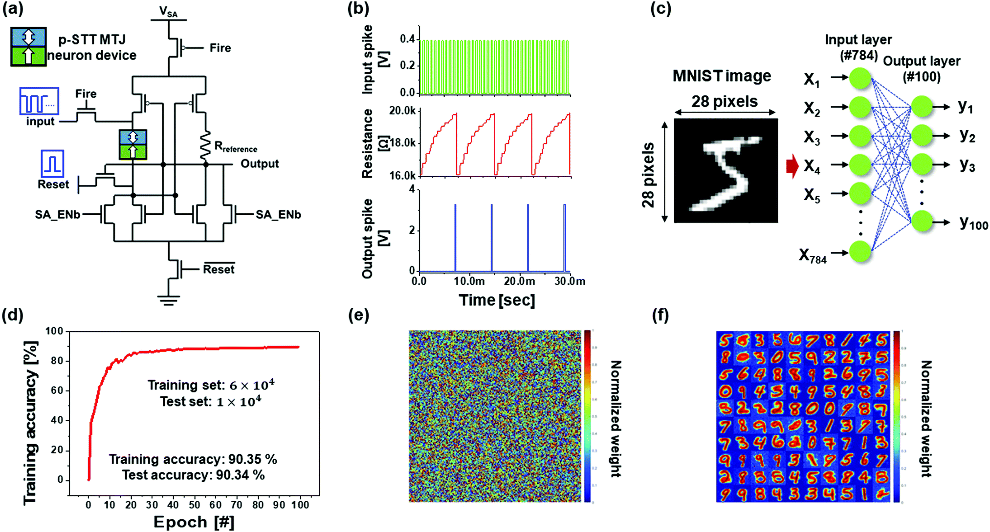
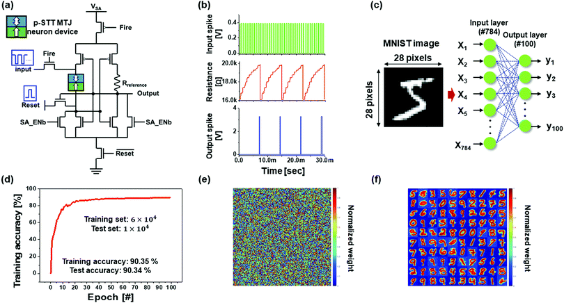
To achieve a p-STT MTJ neuron with a sensing circuit, referred to as a p-STT MTJ neuron, a p-STT MTJ neuron device was implemented with a sense amplifier composed of seven n-MOSFETs, three p-MOSFETs, and one reference resistor (Rref), as shown in Fig. 4a.23 The parallel resistance of the p-STT MTJ neuron device was scaled up to 16 kΩ, corresponding to a scaled-down neuron device area of 100 × 100 nm2 with an average grain size of 0.935 nm, as shown in Fig. S6a (ESI†). As a result, the dependency of the neuron device resistance on the number of input spikes and spike amplitude was determined at to be on the order of several kΩ, as shown in Fig. S6b (ESI†). An Rref value of 17 kΩ was used to consider the resistance of the parallel (16 kΩ) and anti-parallel (29 kΩ) states with a 100 × 100 p-STT MTJ neuron device, as shown in Fig. S6a (ESI†). A reset pulse with an amplitude of +2 V was applied to the p-STT MTJ neuron device such that the resistance state returned from the anti-parallel to the parallel state, as shown in Fig. S7a (ESI†). The simulation results of our proposed neuron are presented in Fig. 4b. The input spike amplitude was 0.4 V, as shown at the top of Fig. 4b. The anti-parallel resistance of the p-MTJ neuron increased from 16 to 19.9 kΩ as the number of input spikes was increased to 11 spikes, as shown in the middle of Fig. 4b. As soon as the anti-parallel resistance became 19.9 kΩ, an output spike was produced to reset the resistance of the p-MTJ neuron device as it returned to the parallel state, as shown at the bottom of Fig. 4b. Because the characteristic of a p-STT MTJ neuron is a spiking neuron, a single-layer SNN was designed to simulate a neural network composed of the p-STT MTJ neurons shown in Fig. 4a located at each of the 100 output nodes of the neural network. In addition, the 784 input nodes of the neurons were utilized because an MNIST image was constructed with dimensions of 28 × 28 pixels, as shown in Fig. 4c. Moreover, the neural network was implemented with a memristor cross-bar array as synapses between the input and output neurons, as shown in Fig. S7b (ESI†). The characteristics of these synapses (i.e., potentiation or depression) were described by  , as shown in Fig. S8a (ESI†),41,42 and the synaptic weight was updated using a simplified spiking-time-dependent-plasticity (STDP) learning rule with a winner-take-all (WTA) model to train the single-layer SNN, as shown in Fig. S8b (ESI†). It should be noted that the MNIST image should be converted to time-dependent spikes, and a higher pixel intensity at each of the 784 pixels in the MNIST image led to a higher generation probability of spikes. Furthermore, to emulate the p-MTJ neurons, the experimental resistances of the p-STT MTJ neuron devices depending on the input spike amplitude were fitted using the Sweibul function, as shown in Fig. S9 (ESI†). The p-STT MTJ neurons based on the SNN were trained with a 6 × 10⁴ MNIST dataset and tested with a 1 × 10⁴ MNIST dataset. The training accuracy of pattern recognition rapidly increased and saturated as the number of epochs was increased (i.e., one training set of the MNIST dataset). The final training and testing accuracies were 90.35% and 90.43%, respectively, as shown in Fig. 4d. The resistance variation of parallel and anti-parallel states due to size variation was estimated using Monte Carlo simulation with variation ranging from 1 to 10%, as shown in Fig. S10a and b (ESI†). In addition, the integrate behaviour depending on the variation was estimated with Monte Carlo simulation, as shown in Fig. S11 (ESI†). The pattern recognition slightly decreased from 90.4 to 85.7 as the variation was increased to 4%. Furthermore, when the variation became 5%, the accuracy was further decreased to average of 82.5 ± 2%. At variation of 10%, the accuracy dropped to 57.9% with larger fluctuation of ∼ 4.4%. The synaptic weight matrix before and after training is shown in Fig. 4e and f, where the matrix is composed of 10 × 10 parts and each part represents the synaptic weight distribution of the 784 synapses. By comparing the synaptic weight matrix before training with that obtained after training, a specific synaptic weight pattern was found at a specific area of the synaptic matrix after 100 epochs of training using the 6 × 10⁴ MNIST dataset. These results indicate that p-STT MTJ neurons could be utilized for SNNs.
 |
| | Fig. 4 p-STT MTJ neuron and pattern recognition simulation. (a) p-STT neuron being consisted of 1 p-STT neuron device, 7 nMOSFETs, 3 p-MOSFETs, and 1 reference resistance (Rref), (b) input spike, simulated integrated resistance, and output spike as a function of the input spike number, (c) schematic of single-layer spiking neural network using p-STT MTJ neurons, (d) pattern recognition accuracy as a function of epoch, and normalized synaptic weight matrix (e) before and (f) after 100 epoch of training. | |
Conclusions
A neuron was constructed using a p-STT MTJ neuron device and a sensing amplifier circuit, which exhibited typical integrate-and-fire characteristics as a spiking neuron. The resistance of this system increased with the number of input spikes, and the resistance changed from a parallel to an anti-parallel state between the ferromagnetic free layer and pinned layer of the p-STT MTJ neuron device. For practical neuron applications, a higher resistance sensing margin (i.e., the resistance difference of the p-STT MTJ neuron device between the no-input-spikes and integrated-input-spikes conditions) is required. The sensing margin of the p-STT MTJ neuron device was strongly dependent on the input spike amplitude. In addition, it was found that a larger average nanoscale grain size of the MgO tunnelling barrier in the p-STT MTJ neuron device led to a higher resistance sensing margin, although the nanoscale thickness of the MgO tunnelling barrier (i.e., 1.15 nm) was the same for all p-STT MTJ neuron devices. Pattern-recognition simulations using an SNN were conducted, which demonstrated the feasibility of a neuron using a p-STT MTJ neuron device and sensing amplifier in SNN applications. In particular, this type of neuron may be well-suited for use in highly integrated neuromorphic chips and with low power consumption (i.e., ∼2.4 pJ per spike with 20 nm p-STT MTJ neuron devices). This may be achieved because a neuron using a p-STT MTJ neuron device requires only seven n-MOSFETs, three p-MOSFETs, and one reference resistor. Further work is needed to explore the influence of the thermal effect on the integrate behaviour for practical applications.
Author contributions
J. U. Baek and J. G. Park conceived and designed the study. J. U. Baek and J. Y. Choi fabricated all patterns and carried out experiments, with the help of J. G. Park. Contributions to the measurements were made by J. U. Baek, H. S. Jun, J. C. Kim, Y. H Choi and H. T Seo. And D. W. Kim, D.S. Woo, W. S. Yi and J. J. Kim conducted a simulation of pattern recognition test. All authors contributed to discussions regarding the research. J. U. Baek, J. Y. Choi and J. G. Park wrote the manuscript.
Conflicts of interest
There are no conflicts to declare.
Acknowledgements
This work was supported by the National Research Foundation of Korea (NRF) grant funded by the Korea Government (MSIT) (No. 2016M3A7B4910249), National R&D Program through the National Research Foundation of Korea(NRF) funded by Ministry of Science and ICT(2021M3F3A2A01037733) the Brain Korea 21 PLUS Program in 2014.
Notes and references
- L. J. Gentet, G. J. Stuart and J. D. Clements, Biophys. J., 2000, 79(1), 314–320 CrossRef CAS PubMed.
- G. Indiveri, B. Linares-Barranco, R. Legenstein, G. Deligeorgis and T. Prodromakis, Nanotechnology, 2013, 24(38), 384010 CrossRef PubMed.
- S. Dutta, V. Kumar, A. Shukla, N. R. Mohapatra and U. Ganguly, Sci. Rep., 2017, 7(1), 1–7 CrossRef PubMed.
- T. Tuma, A. Pantazi, M. Le Gallo, A. Sebastian and E. Eleftheriou, Nat. Nanotechnol., 2016, 11(8), 693 CrossRef CAS PubMed.
- J. Grollier, D. Querlioz and M. D. Stiles, Proc. IEEE, 2016, 104(10), 2024–2039 Search PubMed.
- A. Sengupta, P. Panda, P. Wijesinghe, Y. Kim and K. Roy, Sci. Rep., 2016, 6(1), 1–8 CrossRef PubMed.
- Y. Shim, S. Chen, A. Sengupta and K. Roy, Sci. Rep., 2017, 7(1), 1–9 CrossRef CAS PubMed.
-
G. Srinivasan, A. Sengupta and K. Roy, Design, Automation & Test in Europe Conference & Exhibition (DATE), 2017, pp. 530–535 DOI:10.23919/DATE.2017.7927045.
- J. Torrejon, M. Riou, F. A. Araujo, S. Tsunegi, G. Khalsa, D. Querlioz, P. Bortolotti, V. Cros, K. Yakushiji and A. Fukushima, Nature, 2017, 547(7664), 428–431 CrossRef CAS PubMed.
- A. Mizrahi, T. Hirtzlin, A. Fukushima, H. Kubota, S. Yuasa, J. Grollier and D. Querlioz, Nat. Commun., 2018, 9(1), 1–11 CrossRef CAS.
- A. Kurenkov, S. DuttaGupta, C. Zhang, S. Fukami, Y. Horio and H. Ohno, Adv. Mater., 2019, 31(23), 1900636 CrossRef PubMed.
- J. W. Jang, B. Attarimashalkoubeh, A. Prakash, H. Hwang and Y. H. Jeong, IEEE Trans. Electron Devices, 2016, 63(6), 2610–2613 CAS.
- A. Mondal and A. Srivastava, ACM Journal on Emerging Technologies in Computing Systems (JETC), 2019, 16(1), 1–27 Search PubMed.
- V. Milo, G. Malavena, C. M. Compagnoni and D. Ielmini, Materials, 2020, 13(1), 166 CrossRef CAS PubMed.
-
D. Zhang, L. Zeng, Y. Zhang, W. Zhao and J. O. Klein, IEEE/ACM International Symposium on Nanoscale Architectures (NANOARCH), 2016, pp. 173–178 DOI:10.1145/2950067.2950105.
- C. M. Liyanagedera, A. Sengupta, A. Jaiswal and K. Roy, Phys. Rev. Appl., 2017, 8(6), 064017 CrossRef.
-
G. Hu, M. Gottwald, Q. He, J. Park, G. Lauer, J. Nowak, S. Brown, B. Doris, D. Edelstein and E. Evarts, IEEE International Electron Devices Meeting (IEDM), 2017, pp. 38.3.1–38.3.4 Search PubMed.
- V. Ostwal, P. Debashis, R. Faria, Z. Chen and J. Appenzeller, Sci. Rep., 2018, 8(1), 1–8 CAS.
- K. Kondo, J. Y. Choi, J. U. Baek, H. S. Jun, S. Jung, T. H. Shim and J. G. Park, J. Phys. D: Appl. Phys., 2018, 51(50), 504002 CrossRef.
- R. Zand, K. Y. Camsari, S. Datta and R. F. DeMara, ACM Journal on Emerging Technologies in Computing Systems (JETC), 2019, 15(2), 1–22 CrossRef.
-
F. X. Liang, P. Sahu, M. H. Wu, J. H. Wei, S. S. Sheu and T. H. Hou, International Symposium on VLSI Technology, Systems and Applications (VLSI-TSA), 2020, pp. 151–152 Search PubMed.
-
C. C. Chang, M. H. Wu, J. W. Lin, C. H. Li, V. Parmar, H. Y. Lee, J. H. Wei, S. S. Sheu, M. Suri and T. S. Chang. 56th ACM/IEEE Design Automation Conference (DAC), 2019, pp. 1–6 Search PubMed.
- D. W. Kim, W. S. Yi, J. Y. Choi, K. Ashiba, J. U. Baek, H. S. Jun, J. J. Kim and J. G. Park, Front. Neurosci., 2020, 14, 309 CrossRef PubMed.
- M. Suzuki, A. Yasui, Y. Kotani, N. Tsuji, T. Nakamura and S. Hirosawa, Acta Mater., 2016, 106, 155–161 CrossRef CAS.
- D. Y. Lee, H. T. Seo and J. G. Park, J. Mater. Chem. C, 2016, 4(1), 135–141 RSC.
- H. Yang, M. Chshiev, B. Dieny, J. Lee, A. Manchon and K. Shin, Phys. Rev. B: Condens. Matter Mater. Phys., 2011, 84(5), 054401 CrossRef.
- W. Shen, D. Mazumdar, X. Zou, X. Liu, B. Schrag and G. Xiao, Appl. Phys. Lett., 2006, 88(18), 182508 CrossRef.
- K. S. Chae, D. Y. Lee, T. H. Shim, J. P. Hong and J. G. Park, Appl. Phys. Lett., 2013, 103(16), 162409 CrossRef.
- Y. Takemura, D. Y. Lee, S. E. Lee and J. P. Park, Nanotechnology, 2016, 27(48), 485203 CrossRef PubMed.
- J. Y. Choi, D. G. Lee, J. U. Baek and J. G. Park, Sci. Rep., 2018, 8(1), 1–7 Search PubMed.
- S. E. Lee, J. U. Baek and J. G. Park, Sci. Rep., 2017, 7(1), 1–9 CrossRef PubMed.
- D. Y. Lee, S. E. Lee, T. H. Shim and J. G. Park, Nanoscale Res. Lett., 2016, 11(1), 1–7 CrossRef PubMed.
- S. E. Lee, Y. Takemura and J. G. Park, Appl. Phys. Lett., 2016, 109(18), 182405 CrossRef.
- S. E. Lee, T. H. Shim and J. G. Park, NPG Asia Mater., 2016, 8(11), e324–e324 CrossRef CAS.
- D. Y. Lee, S. H. Hong, S. E. Lee and J. G. Park, Sci. Rep., 2016, 6(1), 1–9 CrossRef PubMed.
- K. Lee, J. J. Sapan, S. H. Kang and E. E. Fullerton, J. Appl. Phys., 2011, 109(12), 123910 CrossRef.
- S. Yuasa and D. Djayaprawira, J. Phys. D: Appl. Phys., 2007, 40(21), R337 CrossRef CAS.
- M. T. Le, Y. U. Sohn, J. W. Lim and G. S. Choi, Mater. Trans., 2010, 51(1), 116–120 CrossRef CAS.
- K. Y. Chan and B. S. Teo, Microelectron. J., 2007, 38(1), 60–62 CrossRef CAS.
- K. Y. Chan and B. S. Teo, Microelectron. J., 2006, 37(10), 1064–1071 CrossRef CAS.
- M. Ziegler, C. Riggert, M. Hansen, T. Bartsch and H. Kohlstedt, IEEE transactions on biomedical circuits and systems, 2015, 9(2), 197–206 Search PubMed.
- M. Hansen, F. Zahari, M. Ziegler and H. Kohlstedt, Front. Neurosci., 2017, 11, 91 Search PubMed.
Footnotes |
| † Electronic supplementary information (ESI) available. See DOI: 10.1039/d1ma00862e |
| ‡ Both authors contributed equally to this manuscript. |
|
| This journal is © The Royal Society of Chemistry 2022 |
Click here to see how this site uses Cookies. View our privacy policy here. 
 Open Access Article
 This Open Access Article is licensed under a Creative Commons Attribution-Non Commercial 3.0 Unported Licence
 a,
Ji-Chan
Kim
b,
Han-Sol
Jun
a,
Dae-Seong
Woo
a,
Ji-Chan
Kim
b,
Han-Sol
Jun
a,
Dae-Seong
Woo
 , of the p-STT MTJ neuron devices depending on the MgO sputtering power was measured using different pulse widths (1 μs, 10 μs, 100 μs, 1 ms, and 10 ms), where Ic is the threshold current, Ic0 is the switching threshold current at 0 K, Eb is the switching energy barrier between the P and AP states, τpw is the pulse width, and τ0 (i.e., 1 ns) is the attempt time, as shown in Fig. 1c. The switching currents for reset (i.e., 6.5 mA) and set (i.e., −10.2 mA) conditions were the lowest at 320 W, which is associated with the dependencies of the f.c.c. crystallinity, grain size and distribution, and surface roughness of the MgO tunnelling barrier sputtering-power.36–38 The current flowing through the MTJ can be divided by two different currents. One is the coherent tunnelling current of the MTJ inside the MgO grain, and the other is the leakage current through the grain boundary. At smaller grain sizes with average of 0.418 nm, the leakage current would take a larger proportion of the current, so it requires more current to switch the CoFeB free layer. As the grain size increases to 0.935 nm, the overall grain boundary area decreases which would increase the proportion of the tunnelling current, so the switching current was reduced. At larger grain size with average of 1.141 nm (i.e., 350 W), the switching current was increased because the coherent tunnelling was reduced as the roughness increased with the MgO sputtering power which reduces the interfacial PMA. Generally, a higher resistance difference (i.e., the difference between the antiparallel and parallel resistances) and lower switching current result in better integrate characteristics for p-STT MTJ neuron devices.23 Therefore, the dependencies of the TMR ratio and switching current on the sputtering power would directly affect the integrate behaviour of p-STT MTJ neuron devices because the MgO sputtering power principally influences the f.c.c. crystallinity and grain size distribution.25
 , as shown in Fig. S8a (ESI†),41,42 and the synaptic weight was updated using a simplified spiking-time-dependent-plasticity (STDP) learning rule with a winner-take-all (WTA) model to train the single-layer SNN, as shown in Fig. S8b (ESI†). It should be noted that the MNIST image should be converted to time-dependent spikes, and a higher pixel intensity at each of the 784 pixels in the MNIST image led to a higher generation probability of spikes. Furthermore, to emulate the p-MTJ neurons, the experimental resistances of the p-STT MTJ neuron devices depending on the input spike amplitude were fitted using the Sweibul function, as shown in Fig. S9 (ESI†). The p-STT MTJ neurons based on the SNN were trained with a 6 × 10⁴ MNIST dataset and tested with a 1 × 10⁴ MNIST dataset. The training accuracy of pattern recognition rapidly increased and saturated as the number of epochs was increased (i.e., one training set of the MNIST dataset). The final training and testing accuracies were 90.35% and 90.43%, respectively, as shown in Fig. 4d. The resistance variation of parallel and anti-parallel states due to size variation was estimated using Monte Carlo simulation with variation ranging from 1 to 10%, as shown in Fig. S10a and b (ESI†). In addition, the integrate behaviour depending on the variation was estimated with Monte Carlo simulation, as shown in Fig. S11 (ESI†). The pattern recognition slightly decreased from 90.4 to 85.7 as the variation was increased to 4%. Furthermore, when the variation became 5%, the accuracy was further decreased to average of 82.5 ± 2%. At variation of 10%, the accuracy dropped to 57.9% with larger fluctuation of ∼ 4.4%. The synaptic weight matrix before and after training is shown in Fig. 4e and f, where the matrix is composed of 10 × 10 parts and each part represents the synaptic weight distribution of the 784 synapses. By comparing the synaptic weight matrix before training with that obtained after training, a specific synaptic weight pattern was found at a specific area of the synaptic matrix after 100 epochs of training using the 6 × 10⁴ MNIST dataset. These results indicate that p-STT MTJ neurons could be utilized for SNNs.