
 Open Access Article
 This Open Access Article is licensed under a Creative Commons Attribution-Non Commercial 3.0 Unported Licence
Dual-functional inorganic CuSCN for efficient hole extraction and moisture sealing of MAPbI3 perovskite solar cells†
Battula Ramya
Krishna
 abc,
Ganapathy
Veerappan
a,
P.
Bhyrappa
b,
C.
Sudakar
c and
Easwaramoorthi
Ramasamy
*a
abc,
Ganapathy
Veerappan
a,
P.
Bhyrappa
b,
C.
Sudakar
c and
Easwaramoorthi
Ramasamy
*a
aCentre for Solar Energy Materials, International Advanced Research Centre for Powder Metallurgy and New Materials (ARCI), Hyderabad, India. E-mail: easwar@arci.res.in
bDepartment of Chemistry, Indian Institute of Technology Madras, Chennai, India
cMultifunctional Materials Laboratory, Department of Physics, Indian Institute of Technology Madras, Chennai, India
First published on 16th December 2021
Abstract
Most high-performing organic–inorganic hybrid perovskite solar cells (PSCs) are fabricated using expensive organic hole-transporting materials (HTMs). The poor moisture- and thermal-stability of organic HTMs are significant factors contributing to the degradation of PSCs. Inorganic HTMs are promising cost-effective alternatives to achieve high efficiencies with enhanced stability. Here, we report PSC devices fabricated using a MAPbI3 perovskite film made by a one-step solution process and coated with inorganic CuSCN (PSC-CuSCN) and organic spiro-OMeTAD (PSC-spiro) HTMs in an n–i–p device configuration. This device performance is compared with that of the HTM-free (PSC-HTM-free) devices. The as-prepared devices were stored under dark ambient conditions (25 ± 3 °C and 50 ± 10% RH) for 1500 h, and their structural and morphological changes were investigated. The PSC-HTM-free and PSC-spiro devices showed a significant conversion of MAPbI3 to PbI2 phase. In contrast, MAPbI3 retained its perovskite structure in the PSC-CuSCN device and exhibited better photovoltaic performance for more than two months. Fresh PSC-spiro and PSC-CuSCN devices showed similar power conversion efficiencies (PCEs) of around 10%, while the PSC-HTM-free device showed a PCE of 6.1%. To compare the impact of atmospheric conditions on the stability of the device, they were stored under dark ambient conditions, and their performance was recorded for 1500 h. PSC-CuSCN retained nearly 70% of its initial PCE for more than 1500 h, whereas both the PSC-HTM-free and PSC-spiro devices exhibited similar performance degradation and retained only 30% of their initial PCE. The moisture resistance of the CuSCN film is understood from the high water contact angle (100°) between the film and the water droplets. We demonstrate that the inherent stability and the absence of dopants in the inorganic CuSCN HTM decelerate the degradation compared to its organic counterparts.
Introduction
Organic–inorganic hybrid perovskite solar cells (PSCs) have gripped the attention of the solar research community as their power conversion efficiencies (PCEs) accelerated to 25.5% in 2021, in just over a decade.1 Such a high photovoltaic performance has been attributed to good ambipolar charge transporting properties, long carrier recombination lifetimes, high optical absorption of the material in films as thin as 500 nm, and long diffusion lengths.2 The efficiency and flexibility in the choice of materials and substrates with good optoelectronic properties have made PSCs a tough competitor to the prevailing technologies. However, the instability of perovskite materials under atmospheric conditions is holding back PSCs from being commercialized. In a conventional n–i–p device configuration, the absorber material is sandwiched between the electron transport and hole transport layers. Usually, the electron transport layer is an inorganic material, and the hole transport layer is an organic material. The most frequently used perovskite absorber material in solar cells is methylammonium lead triiodide (MAPbI3). The striking feature of the MAPbI3 PSC is its optimum bandgap (1.55 eV) which results in a high open-circuit voltage. Hence, in this study, we have employed the workhorse material of the PSC, MAPbI3, as the absorber material.Spiro-OMeTAD or spiro is the most commonly employed hole transporting material (HTM) in conventional PSCs due to its high conductivity. This can be attributed to the extensively employed dopants (bis(trifluoromethane), sulfonimide lithium salt (LiTFSI), and tert-butyl pyridine (t-BP)), which intensify the free carrier generation.3 However, its application is restricted due to high cost and dopant infiltration into the ETM layer, affecting its charge extraction capability leading to hysteresis and instability.3,4 CuSCN has emerged as a stable HTM to replace spiro as it exhibits good chemical stability. With good transparency in the visible and near-infrared regions, appropriate band positions of CuSCN based devices show matching efficiencies. Furthermore, solution based low-temperature processability, cost-effectiveness, and reproducibility have made industrial viability feasible.
Ito et al. first reported the use of CuSCN as a HTM for n–i–p configured MAPbI3 based PSCs.5 They demonstrated a PCE of 4.85%, with 40% retention in PCE after 16 h when stored under ambient conditions at a relative humidity (RH) of 30–90%.5 In another study, Ito et al. studied the degradation under the light illumination of MAPbI3 PSCs using a CuSCN HTM. By incorporating the Sb2S3 layer at the TiO2-perovskite interface, they obtained 5.03% PCE with 65% retention in PCE when exposed continuously to AM 1.5 G irradiation for 12 h.6 However, the effect of CuSCN on device stability was not reported. Baranwal et al. studied the influence of a CuSCN HTM on non-vacuum carbon-based device performance and stability. They reported 12.4% PCE with 68% PCE retention in the CuSCN-incorporated carbon-based device for 4500 h when stored in the dark under ambient conditions.7
Few studies in the literature have explored CuSCN as a HTM in metal cathode, MAPbI3 based PSCs; however, emphasis on device stability is scarce.8–10 Liu et al. reported the stability of the CuSCN HTM in MAPbI3 based PSCs using the Al2O3 mesoporous electron transport layer and compared it with the spiro HTM at elevated temperatures.11 A PCE of 13% for the CuSCN device and 14% for the spiro device were demonstrated. The CuSCN cells encapsulated with a polymeric material were shown to be stable, even at high temperatures of 85 °C and at 50% RH for 1080 h, with 77% retention in PCE.11 Without encapsulation, the device stability reduced to 50% within one day. This was shown to be inferior to the spiro device, which retained less than 28% PCE over 45 days. Zhou et al. studied the effect of CuSCN on MAPbI3 based PSCs wherein devices were sandwiched with macromolecules (CRA-TPA or poly-TPD) between the CuSCN and Ag back contact. They reported 11.97% and 10.36% PCEs for the poly-TPD and CRA-TPA macromoleculues, which are two times higher than that of the control device tested without any macromolecules (PCE of 5.96%). A PCE retention of 70–80% at 25 °C and 50% RH was reported only when an additional triphenylamine layer was introduced. Without this layer, the device degraded within 5 days.12 Yang et al. studied the impact of spiro and CuSCN on MAPbI3 based PSCs. In their study, the MAPbI3 layer was modified with various functional molecules to enhance the stability of the devices. A mixture of 3-pyridyl isothiocyanate (Pr-ITC) and phenylene-1,4-diisothiocyanate (Ph-DITC) has two functional groups to interact with the perovskite as well as the CuSCN layer. An average efficiency of 18.5% was reported for the CuSCN device and 19% for the spiro device. The spiro device retained 50% and the CuSCN device retained 86% PCE for 200 days at 25 °C and 30 ± 5% RH under ambient conditions due to the specific interfacial treatment.13 Yang et al. compared the stability of the spray deposited CuSCN and spin-coated spiro devices on MAPbI3 based PSCs with 17% and 18% PCEs, respectively.14 Their studies demonstrated that the CuSCN based device retained more than 94% of its PCE for 100 days, whereas the spiro-based device retained 70% of its PCE when stored at an RH of 30%.
Other than the MAPbI3 absorber, CuSCN has also been employed in a few other perovskite absorbers where the superior stability of CuSCN has been reported.15–17 However, modification in the perovskite or the HTM layer was inevitable. Here, we explore the CuSCN layer's dual function as a HTM and moisture sealant and correlate it with the device performance and stability in MAPbI3 based devices.18–22 Also, the aging characteristics of efficient working devices for more than 1500 h under ambient conditions (25 ± 3 °C and 50 ± 10% RH ) without interfacial and perovskite compositional modifications are not reported. In this study, we have investigated (i) the MAPbI3 film formation by a one-step method, without any modifications of the MAPbI3 perovskite or charge transport layers, and the structural and morphological evolution of the devices when stored under ambient conditions for 1500 h; (ii) the device fabrication in an n–i–p configuration using an FTO/compact TiO2/mesoporous TiO2/MAPbI3/HTM(spiro/CuSCN/HTM free)/Au architecture; (iii) the aging of the devices at 25 ± 3 °C and 50 ± 10% RH under ambient conditions for 1500 h. CuSCN HTM based PSC devices are found to have superior stability than spiro devices without compromising on the performance.
Experimental
A. Chemicals used
Titaniumbis(acetylacetonate) di-isopropoxide (75 wt% in isopropanol), hydroiodic acid (57 wt% in H2O), hydrochloric acid (37 wt% in H2O), diethyl ether (99.0%), toluene (99.8% anhydrous), lead iodide (PbI2, 99%), 2-propanol (98%), N,N-dimethylformamide (DMF, 99.8%), dimethyl sulfoxide (DMSO, 99.9%), 1-butanol (99.8%), 2,2′,7,7′-tetrakis[N,N-di(4-methoxyphenyl)amino]-9,9′-spirobifluorene (spiro, >99%), 4-tert-butylpyridine (t-BP) (98%) and LiTFSI (≥99%) were purchased from Sigma-Aldrich. Methylamine (40% in methanol) was purchased from TCI Chemicals.B. Device fabrication
TiO2 coated FTO electrodes were prepared as reported in our earlier work.23 MAI was prepared as reported by Im et al.24 To 28 mL of methylamine in a round bottom flask kept at 0 °C, 30 mL of HI was added slowly. After 2 h of stirring, the salt was precipitated at 60 °C in a rotary vacuum evaporator, and washed with diethyl ether 3–4 times to remove the traces of HI. Finally, the MAI salt was dried in a vacuum for 18 h at 60 °C.MAPbI3 films were deposited by a one-step process; 461 mg of PbI2 and 159 mg of MAI were taken in a mixed solvent of 600 mg of dimethylformamide (DMF) and 78 mg of dimethyl sulfoxide (DMSO). This solution was spin-coated onto TiCl4 treated TiO2 substrates at 4000 rpm for 25 s with 100 μL of toluene antisolvent dripped in the last 15 s. The films were annealed at 60 °C for 1 min and 100 °C for 2 min to ensure the formation of a crystalline MAPbI3 film. The organic HTM was prepared by dissolving 75.2 mg of spiro-OMeTAD in 1 mL of chlorobenzene, to this 28.8 μL of t-BP and 17.5 μL of LiF (520 mg in 1 mL of acetonitrile) were added and stirred until completely dissolved. The inorganic HTM was prepared by dissolving 35 mg of CuSCN in 1 mL of diethyl sulfide and stirred at room temperature until completely dissolved. The perovskite films were then spin-coated with the hole transporting material, followed by the thermal evaporation of Au at a pressure of 10−6 mbar. For the HTM-free architecture, the MAPbI3 films were coated with gold without any HTM deposition. The different device configurations used in the present study, viz., FTO/TiO2/perovskite/Au, FTO/TiO2/perovskite/organic(spiro)HTM/Au and FTO/TiO2/perovskite/inorganic(CuSCN)HTM/Au, are denoted as PSC-HTM-free, PSC-spiro and PSC-CuSCN, respectively.
C. Characterization techniques
The structural characterization of the films was explored using an X-ray diffractometer (D8 Advanced Bruker) with monochromatic Cu-Kα radiation (λ = 1.5406 Å). The surface and cross-sectional morphologies of the perovskite films were analyzed using field emission scanning electron microscopy (FESEM) (ZEISS GeminiSEM 500) along with energy-dispersive X-ray spectroscopy (EDX) for composition analysis. The I–V characteristics of the devices were measured under one sun illumination (AM 1.5) using an AAA solar simulator (Oriel instruments) under ambient conditions. For all stability studies, the samples were stored under dark ambient conditions at 25 ± 3 °C and 50 ± 10% RH for 1500 h.Results and discussion
Fig. 1(a–c) show the different device configurations used in the present study with (spiro and CuSCN) and without the HTM, employing the n–i–p architecture. Fig. 1(d) shows the energy band diagram depicting the charge transfer mechanism in the PSC. When light shines on the perovskite absorber material, free charge carriers are generated and swept away by the respective charge transport layers due to the suitable band alignment and are collected by the front and back contacts. In Fig. 1(d), the energy level positions of both spiro and CuSCN are shown for easy comparison. The valence band edge position of CuSCN is very close to that of the organic HTM. This highlights its suitability as a competitor for efficient hole extraction. Employing spectroscopic characterization, it was found that hole transfer was 3 times higher in CuSCN based PSCs compared to that in spiro-based PSCs due to the strong interactions between the CuSCN-perovskite interface.16,25 Since hybrid perovskite materials are ambipolar, they can selectively transport charge carriers to their respective contacts without the need for a charge transport layer. This study utilized this unique ambipolar property of perovskites to transport holes to the back-contact in the HTM-free device architecture.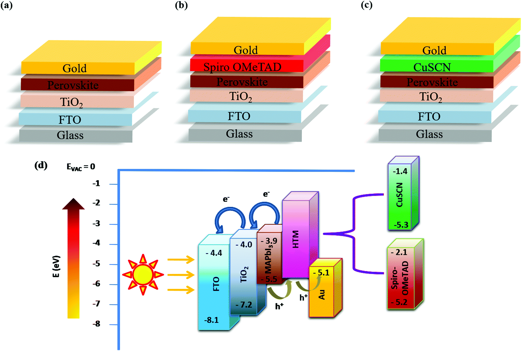 | ||
| Fig. 1 n–i–p Device configurations of (a) PSC-HTM-free, (b) PSC-spiro and (c) PSC-CuSCN. (d) Energy-level diagram highlighting the band edge values of different layers. | ||
Fig. 2 shows the schematic of the device fabrication process (a–c) and cross-sectional FESEM morphologies (d–f) of PSC-HTM-free, PSC-spiro, and PSC-CuSCN, respectively; the details are discussed in the Experimental section. We can see the dense, tightly packed MAPbI3 grains on the mesoporous TiO2 layer with a 600–700 nm combined uniform thickness from the cross-sectional morphologies. The HTM thickness is around 50 nm in both PSC-spiro and PSC-CuSCN (Fig. 2(e and f)), and the metal electrode is around 80 nm to 100 nm in all the cases.
 | ||
| Fig. 2 Schematic of n–i–p PSC device fabrication (a–c) and the corresponding cross-sectional morphologies (d–f) of the respective devices: (a and d) PSC-HTM-free, (b and e) PSC-spiro and (c and f) PSC-CuSCN. | ||
To examine the effect of aging, the as-prepared devices were stored under ambient conditions at 25 ± 3 °C and RH of 50 ± 10% for 1500 h. Structural and morphological changes were studied before and after exposing to the ambient atmosphere. Fig. 3(a–f) show the surface morphological images of the fresh (a–c) and ambient-aged (d–f) PSC-HTM-free, PSC-spiro, and PSC-CuSCN, respectively. The PSC-HTM-free shows compact well-packed grains, as depicted in Fig. 3(a), but multiple pinholes were observed upon ambient-aging for 1500 h, as seen in Fig. 3(d). This is due to the reaction of the MAPbI3 perovskite with atmospheric oxygen and water molecules. This leads to the transformation of MAPbI3 to PbI2 as evidenced from the XRD peak at 2θ = 12.6° (Fig. 4(a)).26 In PSC-spiro, we could see the uniform coverage of the spiro-OMeTAD on the perovskite film (Fig. 3(b)). Features like circular blobs on the film are also noted. A similar phenomenon is also observed in the PSC-CuSCN, as shown in Fig. 3(c). Thermal expansion mismatch between the coating and the underneath layer can prevail, such that, as the film relaxes it leaves circular regions, where the film is bulged out of the substrate. In the worst case, cracks are formed in these regions. Also, evaporation of solvent or other gases such as HI, which is a degradation product from the underneath layer, could also be the reason. This could be avoided by carefully optimizing the absorber and HTM deposition parameters and/or perovskite surface treatment before deposition. From Fig. 3(e), we can see foreign materials segregating to form lumps; this could be due to the penetration of moisture into the perovskite, aided by the hygroscopic nature of the organic HTM dopants.
 | ||
| Fig. 3 FESEM morphological images of (a and d) PSC-HTM-free, (b and e) PSC-spiro and (c and f) PSC-CuSCN, under as-prepared (a–c) and aged (d–f) conditions, respectively. | ||
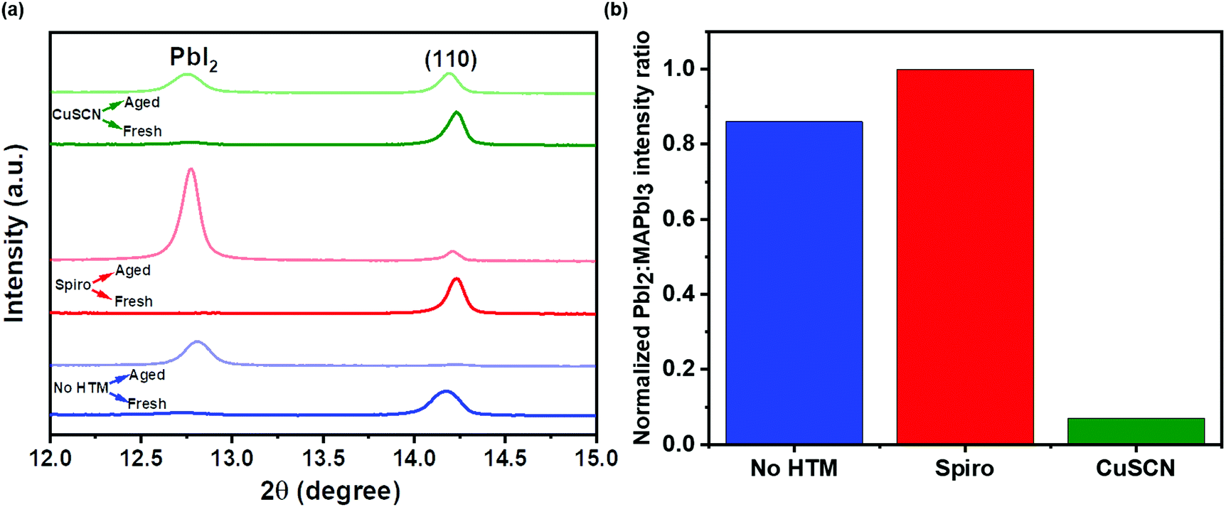 | ||
| Fig. 4 (a) XRD pattern highlighting the PbI2 and (110) peak of MAPbI3 fresh and aged PSC-HTM-free, PSC-spiro and PSC-CuSCN devices. (b) Normalized PbI2:MAPbI3 peak intensity ratios of the aged devicess. | ||
The organic HTM might have partially dissolved when stored under ambient conditions, clearing the shield and aiding easy penetration of moisture and oxygen into the MAPbI3 layer. This has resulted in PbI2 formation, which is also confirmed by the strong diffraction of PbI2 compared to the very weak diffraction of the (110) plane of MAPbI3 as depicted in Fig. 4(b), where the PbI2 and MAPbI3 diffraction intensities are normalized. However, in the PSC-CuSCN, even though there are pinholes in the aged film, as seen in Fig. 3(f), the chemically stable CuSCN layer formed a protective shield over the MAPbI3 film. The little ingress of moisture through the pinholes could have been the source for the degradation of the absorber material. The majority of the MAPbI3 phase remains intact as CuSCN does not interact adversely with the water molecules. This robustness of the inorganic HTM can also be attributed to the water-splitting quality of CuSCN, where the CuSCN layer not only acts as a predator to the water molecules but also alters the water molecules into harmless species.27
Fig. 4(a) shows the structural characterization of the as-prepared and ambient-aged devices highlighting the PbI2 and (110) peak of MAPbI3. The PbI2:MAPbI3 intensity ratios normalized w.r.t. the ratio found in PSC-spiro of the aged devices are plotted in Fig. 4(b). The complete XRD pattern is shown in Fig. S1 of the ESI.† We can see that the MAPbI3 phase primarily oriented in the (110) plane has almost converted to PbI2. It is negligibly present in the aged PSC-HTM-free and PSC-spiro devices. However, the chemical stability of the CuSCN film is reiterated in its structural stability. The CuSCN film prevented the degradation of the perovskite film, and the conversion MAPbI3 to PbI2 is minimal, as shown in Fig. 4(b).
Fig. 5(a–c) show the current–voltage (I–V) characteristics of the as-prepared devices in all three configurations. PSC-spiro devices are fabricated as control to understand the performance and stability of inorganic HTM devices. An HTM-free architecture is employed to understand the impact of the HTM on device performance and stability. The photovoltaic parameters of the device are listed in Table 1. The PSC-HTM-free device exhibited a PCE of 6.1% with an open-circuit voltage (Voc) of 0.8 V, short circuit current density (Jsc) of 17.5 mA cm−2, and a fill factor (FF) of 44%, as shown in Fig. 5(a). The inferior performance highlights the importance of an HTM on the device performance. It is seen that on par with the PSC-spiro device performance of 10%, the PSC-CuSCN performed with 10.1% as shown in Fig. 5(b and c) respectively. The PSC-CuSCN showed a Voc of 0.93 V, Jsc of 17.2 mA cm−2, and a FF of 63%, while the PSC-spiro showed a Voc of 1 V, Jsc of 19.4 mA cm−2 and a FF of 51%. Comparing the performances of PSC-CuSCN and PSC-spiro, we observe a slight decrease in Voc and Jsc in the PSC-CuSCN. The increase of Voc in PSC-spiro can be attributed to the additives in spiro (mainly t-BP), which play a crucial role in Voc enhancement.14 The decrease of Jsc in PSC-CuSCN can be attributed to the fractional dissolution of the CuSCN and MAPbI3 layers leading to an amorphous phase hampering the movement of charges.28 However, the combined detrimental effect of Voc and Jsc in PSC-CuSCN is nullified by the improvement in FF. This can be due to the uniform, well-adhered CuSCN film negating any shunting pathways for charge extraction.
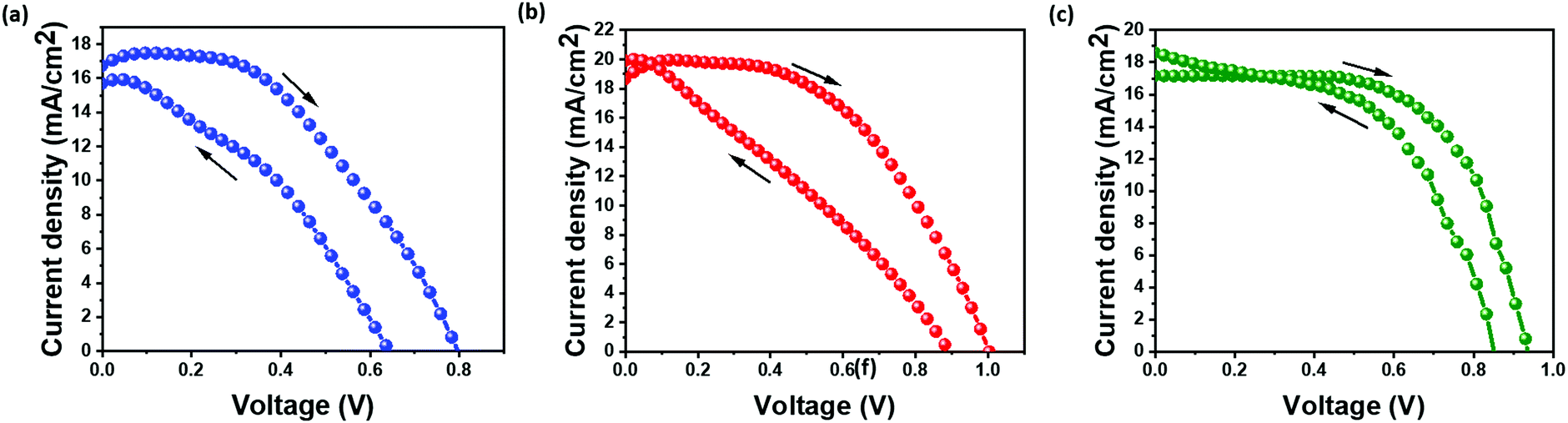 | ||
| Fig. 5 I–V characteristics of the as-prepared (a) PSC-HTM-free, (b) PSC-spiro and (c) PSC-CuSCN. | ||
| Device ID | Duration (h) | V oc (V) | J sc (mA cm−2) | FF (%) | PCE (%) | HI | Retention in PCE (%) |
|---|---|---|---|---|---|---|---|
| PSC-HTM-free | 1 | 0.8 | 17.5 | 44 | 6.1 | 0.3 | — |
| 1350 | 0.4 | 7.3 | 35 | 1 | 0.24 | 16 | |
| PSC-spiro | 1 | 1 | 19.4 | 51 | 10 | 0.45 | — |
| 1500 | 0.5 | 8.4 | 39 | 2.7 | 0.22 | 27 | |
| PSC-CuSCN | 1 | 0.93 | 17.2 | 63 | 10.1 | 0.18 | — |
| 1500 | 0.9 | 13.5 | 58 | 6.9 | 0.36 | 68 |
Hysteresis is majorly caused due to the unbalanced charge extraction rates at the perovskite/ETL and perovskite/HTM interfaces.29 Since the electron mobility is better than the holes, the holes are more often left behind to accumulate in the device. The pronounced hysteresis effect can be seen for PSC-HTM-free and PSC-spiro compared to PSC-CuSCN. The energy offset between the valence band (VB) level of the perovskite and the highest occupied molecular orbital (HOMO) energy level of the spiro is higher than the VBs of the perovskite and CuSCN, as depicted in Fig. 1(d). This energy level alignment facilitates better charge extraction, reduced charge accumulation and recombination, leading to reduced hysteresis in PSC-CuSCN. Also, the number of charges trapped at the perovskite/Au and perovskite/spiro interfaces is much higher than that at the perovskite/CuSCN interface. Hence, the trapped charges can be released faster when the bias is reversed. Compared to PSC-HTM free and PSC-spiro, this leads to better charge extraction at the perovskite/CuSCN interface.30
After the devices were fabricated and tested, they were left under ambient conditions (25 ± 3 °C and 50 ± 10% RH) for 1500 h. The photovoltaic parameters were recorded at regular intervals, and the changes in the parameters as a function of storage time are plotted normalized w.r.t. to the initial values (Fig. 6). The parameters for fresh and aged devices are listed in Table 1. The I–V plots of aged devices in the forward and reverse bias are shown in Fig. S2 of the ESI.† The Voc and FF have not significantly been affected during the aging process, as shown in Fig. 6(a and c), respectively. However, we can see that the PCE shown in Fig. 6(d) majorly follows the trend observed in the Jsc as seen in Fig. 6(b). From Fig. 6(d), we can infer that in the PSC-HTM-free and PSC-spiro devices, the performance has deteriorated dramatically due to the drastic drop in all the photovoltaic parameters. In contrast, in the case of PSC-CuSCN, we have observed that even though there is a slight drop in Jsc, Voc and FF were more or less unaffected. This decrease in Jsc is mainly due to the conversion of MAPbI3 to an amorphous and optically inactive PbI2 phase in the PSC-HTM-free and PSC-spiro devices, as depicted in Fig. 4(a). In the case of PSC-HTM-free, there is no layer on the MAPbI3 film to shield it from the attack of moisture and oxygen, whereas for PSC-spiro, the hygroscopic nature of the organic dopants adds up to the already hostile environment.31 The PbI2 formation results in lower absorption leading to inadequate charge generation, hence the reduction in Jsc. Also, during the degradation of MAPbI3 to PbI2, HI leaves as gas from the film surface, potentially forming pin holes.32 These pinholes act as recombination centres and shunting pathways resulting in a reduced FF. Even though this effect is less pronounced, it adds to the overall decrease in PCE of the PSC-HTM-free and PSC-spiro devices. In PSC-CuSCN, the degradation of MAPbI3 to PbI2 is not as significant as its counterparts. This is because of the robust shielding effect of the chemically stable inorganic CuSCN layer protecting the underneath MAPbI3 layer from the adverse effects of atmospheric conditions. We can see that Jsc has not reduced for almost up to 1000 h of storage under ambient conditions showing the chemically inert nature of the CuSCN layer. It was observed that PSC-CuSCN retained ∼70% of its initial PCE, whereas only ∼30% and ∼15% PCE retention was observed in the PSC-spiro and PSC-HTM-free devices, respectively. The degradation effect can also be seen visibly in the pictorial images of Fig. 7, where the colour transformation from brown to yellow is noticed in the PSC-HTM-free and PSC-spiro devices. In contrast, PSC-CuSCN fairly retained its perovskite phase.
 | ||
| Fig. 6 Normalized (a) Voc, (b) Jsc, (c) FF and (d) PCE of the PSC-HTM-free, PSC-spiro and PSC-CuSCN with respect to time when aged under ambient conditions (25 ± 3 °C and 50 ± 10% RH) for 1500 h. | ||
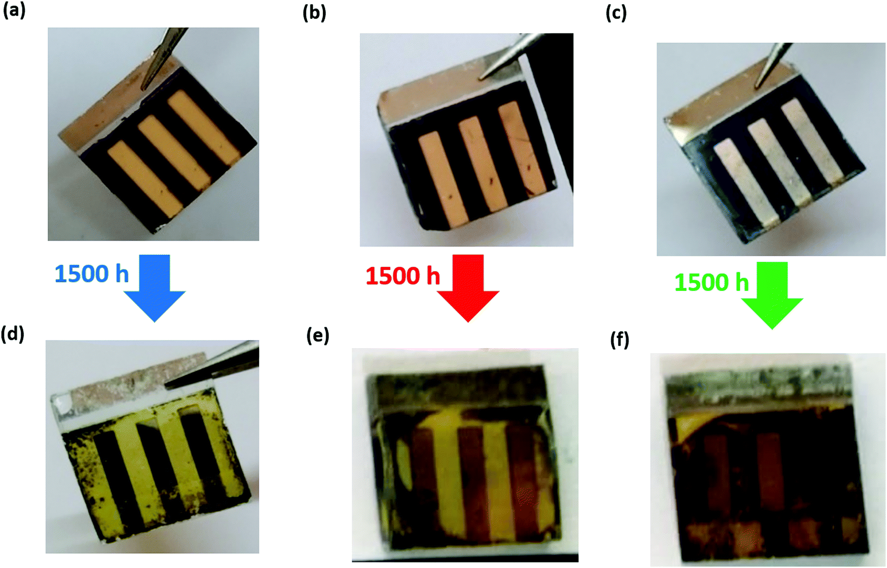 | ||
| Fig. 7 Visual images of PSC-HTM-free (a and d), PSC-spiro (b and e), and PSC-CuSCN (c and f) devices under fresh (a–c) and ambient-aged (d–f) conditions. | ||
The blanketing effect of CuSCN is very pronounced in the real-time images of the as-prepared and aged devices stored under ambient conditions after 1500 h, as shown in Fig. 7. The fresh and aged devices have converted majorly into the PbI2 phase, as evident from Fig. 7(a, b, d and e), due to the susceptibility of the MAPbI3 perovskite absorber layer and the hygroscopic dopants of the organic HTM layer. The films are affected by the moisture and oxygen under ambient conditions. With time, the films convert to their initial precursor state. Only PbI2 remains in the film as an identifiable product and MA escapes as gas. However, the same is not the case in the inorganic CuSCN material, which is more resilient to atmospheric conditions, acting as a capping layer to the underneath perovskite film and thus preventing degradation, as apparent from Fig. 7(c and f).
In order to understand this high moisture stability of PSC-CuSCN, the water contact angle (WCA) of the fabricated devices was recorded to understand the interface between the HTM and perovskite. Fig. 8(a–c) show the WCA on both the non-Au (left-hand side) and the Au covered areas (right-hand side) of the device in all three cases, i.e., PSC-HTM-free, PSC-spiro and PSC-CuSCN, respectively. From Fig. 8(a and b), it is observed that the WCA on the device is more or less similar and close to ∼60°. However, in PSC-CuSCN, as shown in Fig. 8(c), a highly hydrophobic WCA of 100° was recorded, which is nearly a 40% increase in WCA, compared to those of the PSC-HTM-free and PSC-spiro coating layers. The real-time images of the water droplets on all the three respective configurations are also presented in Fig. 8. In the live images, we can see the bead-like water droplets on PSC-CuSCN. The droplets were more flattened on PSC-HTM-free and PSC-spiro, which is also consistent with the WCA measurements. For the PSC-spiro device, the t-BP dopant in spiro increases the polarity of the material leading to better wettability and easier penetration of the moisture into the device.33 The same is the case with PSC-HTM-free due to the polar nature of MAI.34 On the contrary, the non-polar surfaces of CuSCN make the cohesion forces in the water molecules dominate the adhesion forces with the substrate leading to a high contact angle making it hydrophobic.35 Interestingly, the WCAs recorded on the Au strip of the device were also found to be affected by the layer underneath, as depicted in the right-hand images of Fig. 8(a–c). Such observation is not reported so far. It was seen that there is a significant improvement in the WCA on the Au strip compared to the film in all the three cases, highlighting the metal cathode's robustness to moisture penetration. However, the exact reason for this behaviour could not be understood entirely. There is a good chance that the underneath surface influences the WCA of the Au layer.36 For better understanding, the homogeneity and composition of the Au layer on the device were analyzed by FESEM and EDX, as shown in Fig. S3(a and b) (ESI†), respectively. It was found that the Au layer is homogenous and that the underneath layer's nanostructure can influence the WCA on the Au surface. There is an excellent scope to carry out studies in this direction of how the HTM-Au interface prevents moisture penetration into the device. The high WCAs, as observed in Fig. 8(c), were reported for ultra-hydrophobic fluorine-based 2D/3D perovskite materials where the devices were stable for 1000 h when stored at 40% RH.37 Here, we observe a similar trend without modifying the perovskite material or the CuSCN layer for highly stable devices retaining 30% of their initial PCE for over 1500 h when stored at 50 ± 10% RH. The CuSCN–Au interface, which is known as a source of degradation, is not evidenced in this study, and the reason for degradation is due to the MAPbI3–HTM interface. Hence, no interfacial layer is required, and CuSCN itself is shown to act as a protective layer to the perovskite film.
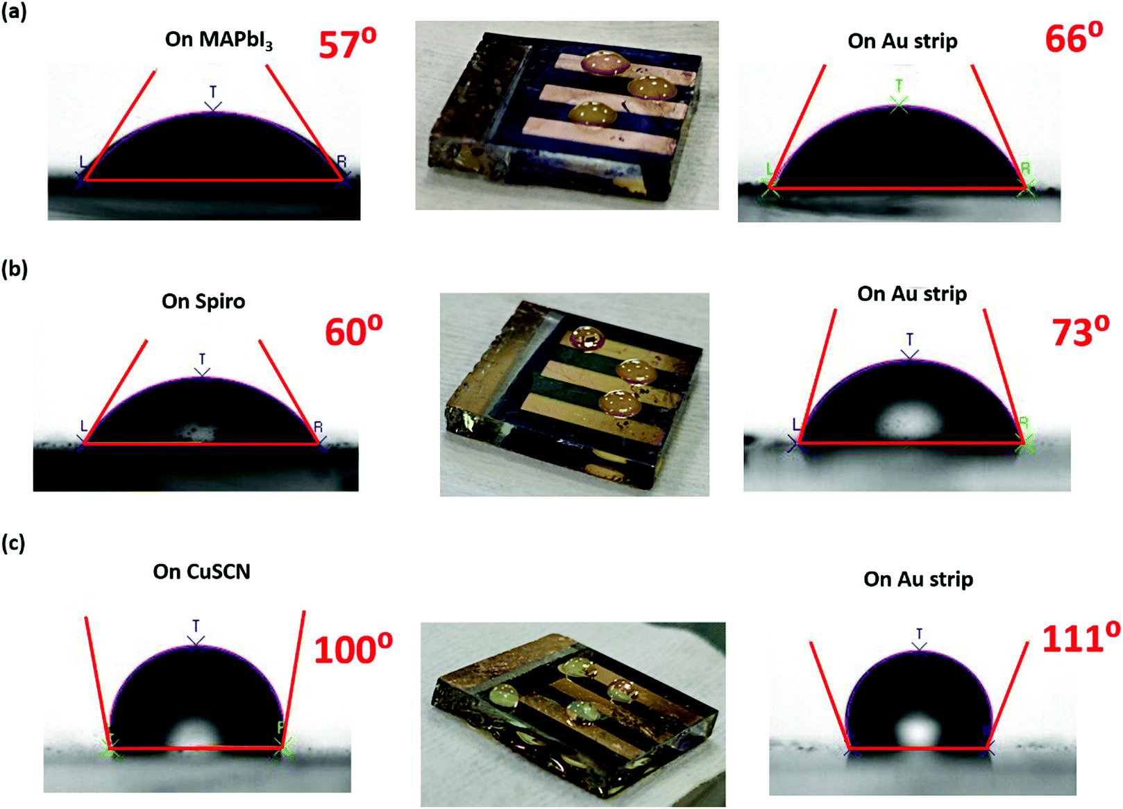 | ||
| Fig. 8 WCA of (a) PSC-HTM-free, (b) PSC-spiro and (c) PSC-CuSCN. The left-hand side image shows the WCA on the non-gold portion of the device, the right-hand side image shows the WCA on the Au strip of the device and the centre image shows the pictorial image of the device with water droplets on the film. | ||
Conclusion
In this work, we have shown the superior dual-functional property of CuSCN, both as a HTM and a moisture resistor, for PSCs. The stability of the one-step processed MAPbI3 PSCs covered with and without HTM, the photovoltaic performance and the aging effect of the PSCs in an n–i–p device configuration were studied in detail. We have successfully fabricated devices using the CuSCN inorganic HTM with a PCE of more than 10%, which is at par with the conventional organic spiro HTM based devices. We have studied the device stability under dark, ambient conditions at 25 ± 3 °C and 50 ± 10% RH for 1500 h. The PCE is majorly dependent on the Jsc of the device. The PSC-HTM-free and PSC-spiro devices showed poor stability, majorly due to the decrease in Jsc owing to the formation of PbI2 when exposed to the ambient atmosphere. In contrast, PSC-CuSCN retained 70% of its initial PCE due to the robust nature of the CuSCN HTM, which is reflected in the devices exhibiting a high water contact angle. We have correlated the degradation of the cells with respect to the device's structural and morphological evolution over time. From the discussions, as evidenced by the XRD, FESEM, and WCA results, it can be reasonably concluded that the primary reason for the instability of the device is the moisture penetration leading to the destruction of the perovskite material. The role of the CuSCN–Au interface here is shown to only act as a protective layer to the perovskite film by preventing moisture ingress, unlike the spiro–Au and MAPbI3–Au interfaces, which facilitate easy penetration. This study shows that blanketing the perovskite with the CuSCN HTM serves as a moisture protection layer without any modification at the interface or in perovskite absorber layer. In this study, the decrease in efficiency with time is only due to the decomposition of the perovskite, which is demonstrated experimentally, and CuSCN has a protective role. Also, a new research direction on the role of the Au metal cathode layer in the stability of PSCs can be further explored with this work as a base. This approach, with further optimization, is promising for fabricating large-area solar cell devices for real-time applications.Author contributions
Conceptualization – Easwaramoorthi Ramasamy, Ganapathy Veerappan, and Ramya Krishna Battula. Data curation – Ramya Krishna Battula and Ganapathy Veerappan. Formal analysis – Ramya Krishna Battula and Easwaramoorthi Ramasamy. funding acquisition – Easwaramoorthi Ramasamy and Ganapathy Veerappan. Investigation – Ramya Krishna Battula, Easwaramoorthi Ramasamy, and Ganapathy Veerappan. Methodology – Ramya Krishna Battula, Ganapathy Veerappan, and Easwaramoorthi Ramasamy. project administration – Easwaramoorthi Ramasamy and Ganapathy Veerappan. resources – Easwaramoorthi Ramasamy and Ganapathi Veerappan. supervision – Easwaramoorthi Ramasamy, Ganapathy Veerappan, C Sudakar, and P Bhyrappa. Validation – Ramya Krishna Battula, Easwaramoorthi Ramasamy, Ganapathy Veerappan, C Sudakar, and P Bhyrappa. Visualization – Easwaramoorthi Ramasamy. writing – original draft – Ramya Krishna Battula. writing – review and editing – Ramya Krishna Battula, Easwaramoorthi Ramasamy, Ganapathy Veerappan, C Sudakar, and P Bhyrappa.Conflicts of interest
There are no conflicts to declare.Acknowledgements
The authors are grateful to the Technical Research Centre project (AI/1/65/ARCI/2014) and the Clean Energy Research Initiative project (DST/TMD/CERI/C247(G)), Department of Science & Technology, Government of India, for funding this work.References
- J. Jeong, M. Kim, J. Seo, H. Lu, P. Ahlawat, A. Mishra, Y. Yang, M. A. Hope, F. T. Eickemeyer, M. Kim, Y. J. Yoon, I. W. Choi, B. P. Darwich, S. J. Choi, Y. Jo, J. H. Lee, B. Walker, S. M. Zakeeruddin, L. Emsley, U. Rothlisberger, A. Hagfeldt, D. S. Kim, M. Grätzel and J. Y. Kim, Pseudo-halide anion engineering for α-FAPbI3 perovskite solar cells, Nature, 2021, 592, 381–385 CrossRef CAS PubMed.
- H. J. Snaith and L. Schmidt-Mende, Advances in Liquid-Electrolyte and Solid-State Dye-Sensitized Solar Cells, Adv. Mater., 2007, 19, 3187–3200 CrossRef CAS.
- T. H. Schloemer, J. A. Christians, J. M. Luther and A. Sellinger, Doping strategies for small molecule organic hole-transport materials: impacts on perovskite solar cell performance and stability, Chem. Sci., 2019, 10, 1904–1935 RSC.
- Z. Li, C. Xiao, Y. Yang, S. P. Harvey, D. H. Kim, J. A. Christians, M. Yang, P. Schulz, S. U. Nanayakkara, C.-S. Jiang, J. M. Luther, J. J. Berry, M. C. Beard, M. M. Al-Jassim and K. Zhu, Extrinsic ion migration in perovskite solar cells, Energy Environ. Sci., 2017, 10, 1234–1242 RSC.
- S. Ito, S. Tanaka, H. Vahlman, H. Nishino, K. Manabe and P. Lund, Carbon-Double-Bond-Free Printed Solar Cells from TiO 2/CH 3 NH 3 PbI 3/CuSCN/Au: Structural Control and Photoaging Effects, ChemPhysChem, 2014, 15, 1194–1200 CrossRef CAS PubMed.
- S. Ito, S. Tanaka, K. Manabe and H. Nishino, Effects of Surface Blocking Layer of Sb2S3 on Nanocrystalline TiO2 for CH3NH3PbI3 Perovskite Solar Cells, J. Phys. Chem. C, 2014, 118, 16995–17000 CrossRef CAS.
- A. K. Baranwal, H. Kanda, N. Shibayama and S. Ito, Fabrication of fully non-vacuum processed perovskite solar cells using an inorganic CuSCN hole-transporting material and carbon-back contact, Sustain, Energy Fuels, 2018, 2, 2778–2787 CAS.
- G. Murugadoss, R. Thangamuthu and S. M. Senthil Kumar, Fabrication of CH3NH3PbI3 perovskite-based solar cells: Developing various new solvents for CuSCN hole transport material, Sol. Energy Mater. Sol. Cells, 2017, 164, 56–62 CrossRef CAS.
- S. Karuppuchamy, G. Murugadoss, K. Ramachandran, V. Saxena and R. Thangamuthu, Inorganic based hole transport materials for perovskite solar cells, J. Mater. Sci.: Mater. Electron., 2018, 29, 8847–8853 CrossRef CAS.
- P. Qin, S. Tanaka, S. Ito, N. Tetreault, K. Manabe, H. Nishino, M. K. Nazeeruddin and M. Grätzel, Inorganic hole conductor-based lead halide perovskite solar cells with 12.4% conversion efficiency, Nat. Commun., 2014, 5, 3834 CrossRef CAS PubMed.
- J. Liu, S. K. Pathak, N. Sakai, R. Sheng, S. Bai, Z. Wang and H. J. Snaith, Identification and Mitigation of a Critical Interfacial Instability in Perovskite Solar Cells Employing Copper Thiocyanate Hole-Transporter, Adv. Mater. Interfaces, 2016, 3, 1600571 CrossRef.
- J. Zhou, P. Liu, Y. Du, W. Zong, B. Zhang, Y. Liu, S. Xu and S. Cao, Evident Enhancement of Efficiency and Stability in Perovskite Solar Cells with Triphenylamine-Based Macromolecules on the CuSCN Hole-Transporting Layer, J. Electron. Mater., 2021, 50, 3962–3971 CrossRef CAS.
- I. S. Yang, S. Lee, J. Choi, M. T. Jung, J. Kim and W. I. Lee, Enhancement of open circuit voltage for CuSCN-based perovskite solar cells by controlling the perovskite/CuSCN interface with functional molecules, J. Mater. Chem. A, 2019, 7, 6028–6037 RSC.
- I. S. Yang, M. R. Sohn, S. Do Sung, Y. J. Kim, Y. J. Yoo, J. Kim and W. I. Lee, Formation of pristine CuSCN layer by spray deposition method for efficient perovskite solar cell with extended stability, Nano Energy, 2017, 32, 414–421 CrossRef CAS.
- M. Jung, Y. C. Kim, N. J. Jeon, W. S. Yang, J. Seo, J. H. Noh and S. Il Seok, Thermal Stability of CuSCN Hole Conductor-Based Perovskite Solar Cells, ChemSusChem, 2016, 9, 2592–2596 CrossRef CAS PubMed.
- N. Arora, M. I. Dar, A. Hinderhofer, N. Pellet, F. Schreiber, S. M. Zakeeruddin and M. Grätzel, Perovskite solar cells with CuSCN hole extraction layers yield stabilized efficiencies greater than 20%, Science, 2017, 358, 768–771 CrossRef CAS PubMed.
- A. Khorasani, M. Marandi, A. Irajizad and N. Taghavinia, A new co-solvent assisted CuSCN deposition approach for better coverage and improvement of the energy conversion efficiency of corresponding mixed halides perovskite solar cells, J. Mater. Sci.: Mater. Electron., 2019, 30, 11576–11587 CrossRef CAS.
- J. He, D. Casanova, W.-H. Fang, R. Long and O. V. Prezhdo, MAI Termination Favors Efficient Hole Extraction and Slow Charge Recombination at the MAPbI 3/CuSCN Heterojunction, J. Phys. Chem. Lett., 2020, 11, 4481–4489 CrossRef CAS PubMed.
- S. S. Mali, J. V. Patil, H. Kim, R. Luque and C. K. Hong, Highly efficient thermally stable perovskite solar cells via Cs:NiO/CuSCN double-inorganic hole extraction layer interface engineering, Mater. Today, 2019, 26, 8–18 CrossRef CAS.
- S. Hou, B. Shi, P. Wang, Y. Li, J. Zhang, P. Chen, B. Chen, F. Hou, Q. Huang, Y. Ding, Y. Li, D. Zhang, S. Xu, Y. Zhao and X. Zhang, Highly efficient bifacial semitransparent perovskite solar cells based on molecular doping of CuSCN hole transport layer, Chin. Phys. B, 2020, 29, 078801 CrossRef CAS.
- P. Xu, J. Liu, J. Huang, F. Yu, R. Zhang, C.-H. Li, Y.-X. Zheng and J.-L. Zuo, Coordination Strategy Driving the Formation of Compact CuSCN Hole-Transporting Layers for Efficient Perovskite Solar Cells, Sol. RRL, 2021, 2000777 CrossRef CAS.
- S. S. Mali, J. V. Patil and C. K. Hong, A ‘Smart-Bottle’ humidifier-assisted air-processed CuSCN inorganic hole extraction layer towards highly-efficient, large-area and thermally-stable perovskite solar cells, J. Mater. Chem. A, 2019, 7, 10246–10255 RSC.
- R. K. Battula, G. Veerappan, P. Bhyrappa, C. Sudakar and E. Ramasamy, Stability of MAPbI 3 perovskite grown on planar and mesoporous electron-selective contact by inverse temperature crystallization, RSC Adv., 2020, 10, 30767–30775 RSC.
- J.-H. Im, I.-H. Jang, N. Pellet, M. Grätzel and N.-G. Park, Growth of CH3NH3PbI3 cuboids with controlled size for high-efficiency perovskite solar cells, Nat. Nanotechnol., 2014, 9, 927–932 CrossRef CAS PubMed.
- K. Pydzińska, J. Karolczak, I. Kosta, R. Tena-Zaera, A. Todinova, J. Idígoras, J. A. Anta and M. Ziółek, Determination of Interfacial Charge-Transfer Rate Constants in Perovskite Solar Cells, ChemSusChem, 2016, 9, 1647–1659 CrossRef PubMed.
- J. B. Patel, R. L. Milot, A. D. Wright, L. M. Herz and M. B. Johnston, Formation Dynamics of CH 3 NH 3 PbI 3 Perovskite Following Two-Step Layer Deposition, J. Phys. Chem. Lett., 2016, 7, 96–102 CrossRef CAS PubMed.
- M. Kim, A. Alfano, G. Perotto, M. Serri, N. Dengo, A. Mezzetti, S. Gross, M. Prato, M. Salerno, A. Rizzo, R. Sorrentino, E. Cescon, G. Meneghesso, F. Di Fonzo, A. Petrozza, T. Gatti and F. Lamberti, Moisture resistance in perovskite solar cells attributed to a water-splitting layer, Commun. Mater., 2021, 2, 6 CrossRef.
- S. Ito, S. Kanaya, H. Nishino, T. Umeyama and H. Imahori, Material Exchange Property of Organo Lead Halide Perovskite with Hole-Transporting Materials, Photonics, 2015, 2, 1043–1053 CrossRef CAS.
- H. Wang, A. Guerrero, A. Bou, A. M. Al-Mayouf and J. Bisquert, Kinetic and material properties of interfaces governing slow response and long timescale phenomena in perovskite solar cells, Energy Environ. Sci., 2019, 12, 2054–2079 RSC.
- Y. Yang, M. T. Hoang, D. Yao, N. D. Pham, V. T. Tiong, X. Wang and H. Wang, Spiro-OMeTAD or CuSCN as a preferable hole transport material for carbon-based planar perovskite solar cells, J. Mater. Chem. A, 2020, 8, 12723–12734 RSC.
- H. Zhang, Y. Shi, F. Yan, L. Wang, K. Wang, Y. Xing, Q. Dong and T. Ma, A dual functional additive for the HTM layer in perovskite solar cells, Chem. Commun., 2014, 50, 5020 RSC.
- J. M. Frost, K. T. Butler, F. Brivio, C. H. Hendon, M. van Schilfgaarde and A. Walsh, Atomistic Origins of High-Performance in Hybrid Halide Perovskite Solar Cells, Nano Lett., 2014, 14, 2584–2590 CrossRef CAS PubMed.
- Z. Hawash, L. K. Ono and Y. Qi, Recent Advances in Spiro-MeOTAD Hole Transport Material and Its Applications in Organic–Inorganic Halide Perovskite Solar Cells, Adv. Mater. Interfaces, 2018, 5, 1700623 CrossRef.
- Z. Wang, L. Qiu, Z. Rao, R. Liang, C. Li, W. Huang and S. Zhang, Polar molecules realignment in CH3NH3PbI3 by strain gradient, Mater. Lett., 2020, 275, 128106 CrossRef CAS.
- P. Pattanasattayavong, V. Promarak and T. D. Anthopoulos, Electronic Properties of Copper(I) Thiocyanate (CuSCN), Adv. Electron. Mater., 2017, 3, 1600378 CrossRef.
- M. E. Abdelsalam, P. N. Bartlett, T. Kelf and J. Baumberg, Wetting of Regularly Structured Gold Surfaces, Langmuir, 2005, 21, 1753–1757 CrossRef CAS PubMed.
- Y. Liu, S. Akin, L. Pan, R. Uchida, N. Arora, J. V. Milić, A. Hinderhofer, F. Schreiber, A. R. Uhl, S. M. Zakeeruddin, A. Hagfeldt, M. I. Dar and M. Grätzel, Ultrahydrophobic 3D/2D fluoroarene bilayer-based water-resistant perovskite solar cells with efficiencies exceeding 22%, Sci. Adv., 2019, 5, eaaw2543 CrossRef CAS PubMed.
Footnote |
| † Electronic supplementary information (ESI) available. See DOI: 10.1039/d1ma00861g |
| This journal is © The Royal Society of Chemistry 2022 |