DOI:
10.1039/D1MA00842K
(Paper)
Mater. Adv., 2022,
3, 1574-1580
High temperature thermo-mechanical properties of praseodymium doped ceria thin films measured two ways†
Received
13th September 2021
, Accepted 19th December 2021
First published on 22nd December 2021
Abstract
The temperature dependence of a mixed ionic electronic conducting (MIEC) material's thermo-chemical expansion coefficient, biaxial modulus, and/or Young's modulus are crucial in determining the internal stress, strain, and/or mechanical stability of the various electrochemical devices (batteries, fuel cells, gas sensors, etc.) utilizing them. This work compares the temperature-dependent thermo-chemical expansion coefficient, biaxial modulus, and Young's modulus of Pr0.1Ce0.9O1.95−δ (10PCO) MIEC thin films obtained using two different techniques: (1) a “dual substrate” technique where in-plane stress measurements were collected on “identical” 10PCO thin films atop two different substrate compositions, and (2) a “dual characterization” technique were out-of-plane strain measurements and in-plane stress measurements were performed on a single sample. Both techniques indicated that from 500 to 700 °C (1) the average 10PCO thermo-chemical expansion coefficient in the (100) plane increased from ∼12.5 to ∼17.5 ppm, (2) the 10PCO biaxial modulus in the (100) plane was roughly constant at ∼300 GPa, and (3) the average 10PCO Young's modulus in the (100) plane was roughly constant at ∼175 GPa.
Introduction
Ceria and doped ceria have been widely used as oxygen exchange materials in solid oxide fuel cells (SOFCs),1 solid oxide electrolysis cells (SOECs),2 solar thermo-chemical cells,3 catalytic converters,4 chemical sensors,5 oxide memristors,6 oxygen separation membranes,7 and other electrochemical devices.8 Due to ceria's point defect chemistry9–11 and low oxygen surface exchange kinetics near room temperature,10,12,13 ceria is most often used several hundred degrees above room temperature. As a result, information on ceria's temperature-dependent thermo-chemical expansion behavior and temperature-dependent elastic properties is critical for determining the internal stress, strain, and mechanical stability of various ceria-based devices. Unfortunately, the difficulty of conducting in situ high-temperature mechanical property measurements has limited the number of reports on ceria's high-temperature mechanical properties.
Hence, this work measured and compared the temperature-dependent thermo-chemical expansion coefficient (α), biaxial modulus (M), and Young's modulus (E) of Pr0.1Ce0.9O1.95−δ (10PCO) thin films obtained using two different techniques. In the first “dual substrate” (DS) technique, α, M, and E were determined from elevated-temperature in-plane stress measurements collected on “identically-produced” 10PCO thin films atop two different substrates with very different thermal expansion coefficients. In the second “dual characterization” (DC) technique, α, M, and E were determined from elevated-temperature out-of-plane strain measurements and in-plane stress measurements performed on a single sample.
Theory
Dual substrate technique overview
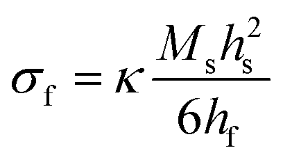
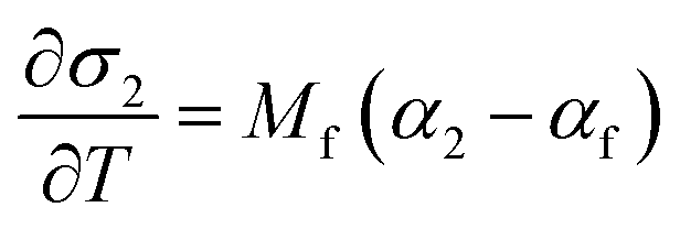
As detailed previously,10,14–16 the “dual substrate” technique determines a film's thermo-chemical expansion coefficient (αf) and a film's biaxial modulus (Mf) generally defined for any material as:| |  | (1) |
| |  | (2) |
respectively (where a is an arbitrary length, T is temperature in Celsius, 25 denotes 25 °C, v is the Poisson's ratio, and the other variables have their previously defined meanings), from the measured instantaneous change in the in-plane biaxial film stress (σf) for a change in temperature (ΔT) for two “identical” films on substrates with very different thermal expansion coefficients (CTE's). This is achieved by plugging the equation for the amount of CTE-mismatch-induced strain in the film (εf) induced by substrate 1 or substrate 2:into the thin film version of Hooke's Law:and differentiating the result to yield two equations, with two unknowns (αf and Mf):| | 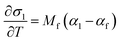 | (5a) |
| | 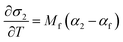 | (5b) |
that can be solved simultaneously for αf and Mf, assuming the substrate thermo-chemical expansion coefficients (α1 and α2) are known. Ef can then be extracted from Mfviaeqn (2) and knowledge of the film's Poisson's ratio.
Dual characterization technique overview
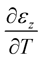
As described previously,17 the “Dual characterization” technique determines a film's αf and Mf through comparison of the out-of-plane film strain (εz) and the in-plane film stress (σf). Specifically, the out-of-plane strain can be expressed as the sum of (1) the thermo-chemical film strain in the out-of-plane direction, and (2) the z-direction Poisson strain caused by in-plane strain induced by a change in temperature (ΔT) and the coefficient of thermal expansion (CTE) mismatch between the film and substrate (αs − αf), via the equation:| | 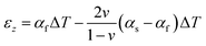 | (6) |
assuming the same directionally-averaged αf in the plane of the film and in the plane perpendicular to the film (which was assumed to the case for the high-temperature, lightly strained (i.e. still cubic)18 (100)-oriented ceria films analyzed here). Differentiating eqn (6) allows αf to be determined from the measured  , the known substrate thermo-chemical expansion coefficient (αs), and a known/assumed vfvia the equation:
| | 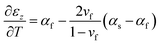 | (7) |
The resulting value for αf, the measured in-plane stress vs. temperature behavior, and the known thermo-chemical expansion coefficient of the substrate can then be plugged into eqn (5a) to yield Mf. As with the DS technique, the film's Young's Modulus, Ef, can then be extracted from Mfviaeqn (2) and knowledge of the film's Poisson's ratio.
Experimental techniques
Thin film fabrication and structural characterization.
Here, 233 nm-thick 10PCO films were produced on either 200 μm-thick (100)-oriented 9.5 mol% yttria doped zirconia or 200 μm-thick (100)-oriented MgO single crystal substrates using the substrate-annealing, target-manufacturing, pulsed laser deposition (PLD), and post-deposition annealing procedures described previously in Ma and Nicholas.10 MgO and YSZ were chosen for their chemical stability with ceria10,19,20 and constant oxygen nonstoichiometry20 (i.e. lack of chemical expansion) at the temperatures/oxygen partial pressures encountered here. Both 10PCO|YSZ and 10PCO|MgO samples were used for the DS measurements, while only 10PCO|YSZ samples (which avoided the potential complexities of MgO hydrating/dehydrating during storage and/or testing) were used for the DC technique measurements. Each film's as-deposited 25 °C preferred crystallographic orientation was examined via XRD survey scans conducted between 20° and 80° with a 0.01° step size and a 1 second dwelling time in air on a Rigaku SmartLab Diffractometer with a 44 kV voltage and a 40 mA current. Each film's as-deposited 25 °C thickness was evaluated from scanning electron microscopy (SEM) images of 5 nm-Pt-coated fractured sample cross-sections taken with a MIRA3 field emission SEM (TESCAN Inc.) operated at 20 kV.
Dual substrate technique measurements
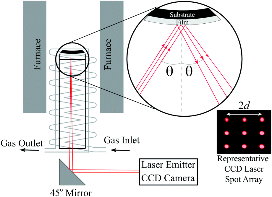
Here, in situ in-plane biaxial film stress measurements were conducted using the Multi-beam optical stress (MOS) sensor shown schematically in Fig. 1. Specifically, since the dense thin films analyzed here all had a film thickness (hf) less than ∼1/1000th of the substrate thickness (hs),20,21 the in-plane film stress could be extracted from the measured bilayer wafer curvature (κ) via Stoney's equation:22,23| |  | (8) |
using hf and hs values measured from scanning electron microscopy cross-sections (such as those shown in Fig. S1 of the ESI†) and the temperature-dependent substrate biaxial modulus (Ms) values obtained from the literature24–26 and shown in Fig. S2 of the ESI.† These in situ curvature measurements were performed using the calibration and experimental equipment setup described in Nicholas.20 As done previously,10 stress vs. temperature measurements were collected in 25 sccm of flowing synthetic air (20% O2–80% Ar) from 700 °C to 280 °C with a 0.2 °C min−1 cooling rate that, as shown in Fig. S3 of the ESI,† was sufficiently slow to ensure that the samples remained in thermal equilibrium while the stress vs. temperature data was collected. Due to the complicated, combined action of thermal and/or chemical expansion of both the film and the substrate on the stress vs. temperature behavior, a third order polynomial (i.e. the lowest order polynomial that adequately captured the sample behavior), and not some physical-model-predicted equation, was used to fit the stress vs. temperature data. The analytical derivatives of these fits were then taken to solve for αf and Mfviaeqn (5a) and (5b). The mathematical error introduced and propagated by this process was estimated using the error analysis described in the ESI† of Ma and Nicholas.10 Since high temperature data on the (Y2O3)0.095(ZrO2)0.905 thermo-chemical expansion coefficient was only available below 600 °C,27 as shown in Fig. S4 and S5 of the ESI,† the 25–700 °C YSZ αs values needed to extract αfviaeqn (7) were also measured on 10PCO-supporting YSZ wafers. Values for the 25–700 °C thermal expansion coefficients of MgO were taken from Suzuki.28
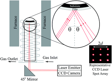 |
| | Fig. 1 Schematic of the multibeam optical stress (MOS) sensor in situ wafer curvature measurement setup used here to perform the film stress vs. temperature measurements. Reproduced from Nicholas20 with permission from Elsevier. | |
Since the 10PCO Ef and vf values in the (100) plane are directionally-dependent (as shown in Fig. S6 of the ESI†) and the Poisson ratio of doped ceria remains relatively constant with temperature,29 here the measured Mf values (which are not directionally dependent in the (100)-plane as shown in Fig. S6 of the ESI†) were converted to directionally-averaged (100)-plane Ef values using eqn (2) by assuming the 0.42 directionally-averaged (100)-plane vf values for room temperature ceria (derived from the C11 = 4.03 × 10¹² dyn cm−2, C22 = 1.05 × 10¹² dyn cm−2, and C44 = 0.06 × 10¹² dyn cm−2 values reported in Nakajima et al.)30 also applied at the temperatures measured here.
Dual characterization technique measurements
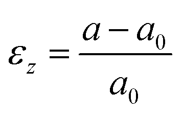
Here, in situ out-of-plane strain measurements were conducted from the X-ray diffraction (XRD)-determined position shift of the (200) 10PCO peak shown in Fig. S7 of the ESI† using the equation:| |  | (9) |
where a was the (200)-determined instantaneous lattice constant of 10PCO, and a0 was (200)-determined room temperature lattice constant at room temperature. These measurements were conducted in air on a Rigaku SmartLab Diffractometer operated at 44 kV and 40 mA. A Rigaku HT1500 hot stage equipped with a platinum sample holder and a R-type thermocouple was used to heat the samples during XRD measurement. After initial XRD measurements at 25 °C, each 10PCO|YSZ sample was heated up to 700 °C with a 5 °C min−1 nominal heating rate and XRD measurements were conducted at 700, 675, 650, 625, 600, 575, 550, 525, and 500 °C from 31∼34° using a 0.01° annular increment and a 1 second dwell time after being thermally equilibrated for 10, 10, 20, 30, 40, 40, 50, and 60 minutes, respectively. At each temperature, at least three measurements were taken to check for, and ensure, that the samples were in thermal and chemical equilibrium. A 1 °C min−1 cooling rate was used between each analysis temperature. As shown in Fig. S7 of the ESI,† at each temperature, the measured XRD peaks were fitted with a Pearson VII function to determine their peak position. This function, which contains a Lorentzian component to account of the theoretically-expected shape of each XRD peak and a Gaussian shape to account for instrument-induced peak broadening31 is commonly used to determine XRD peak positions.32 After solving for αf with these parameters and an assumed 0.42 Poisson ration viaeqn (7), the in-plane strain was calculated viaeqn (3) and the previously described substrate α values. Mf was then determined by comparing this in-plane strain to the in-plane stress determined from in situ wafer curvature measurements via Hooke's Law (eqn (4)). The error introduced by this process was estimated using the error analysis described in Section 2 of the ESI.† As with the Mf values estimated from the DS technique, the directionally-isotropic (100) plane Mf values estimated from this DC technique were converted into directionally-averaged (100)-plane Ef values assuming that the directionally-averaged (100) plane vf average of 0.42 also applied between 500 and 700 °C.
Results and discussion
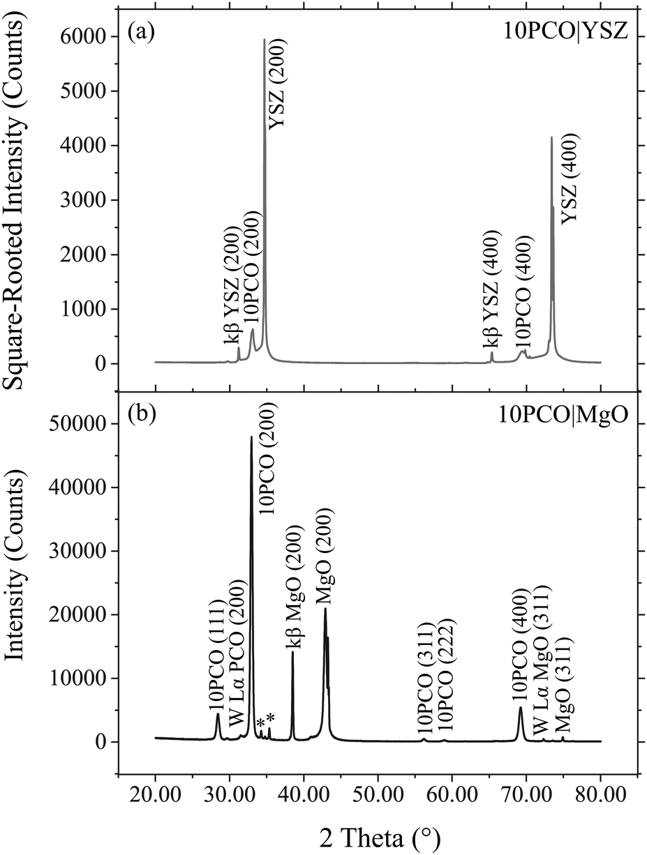
Fig. 2 shows representative XRD survey scans for the 10PCO|YSZ and 10PCO|MgO samples. This data indicates that, for both YSZ and MgO substrates, nearly all the grains in the 10PCO films exhibited a (100) preferred crystallographic orientation. In fact, an analysis made using the (200)![[thin space (1/6-em)]](https://www.rsc.org/images/entities/char_2009.gif) :(111) peak intensity ratios found in Fig. 2, compared to the 28.5:100 (200):(111) peak intensity ratio in JCPDS PDF #34-394 for a collection of randomly-oriented ceria grains, suggests that (a) ∼100 volume% of the PCO grains in the 10PCO|YSZ samples had a (100) orientation, and (b) ∼97 volume% of the PCO grains in the 10PCO|MgO samples had a (100) orientation (while ∼3% volume% had a (111) orientation). Similarly, a more accurate determination made using the integrated peak intensities shown in the pole figure XRD data of Fig. S8 of the ESI† suggests that ∼97 and 86 volume% of the PCO grains on the MgO and YSZ single crystal substrates, respectively, were (100)-oriented. The preferred (100)-orientation of the PCO grains observed here is consistent with the (100) preferred crystallographic orientation ceria has exhibited on YSZ.10,33–37 and MgO19 substrates in the literature.
:(111) peak intensity ratios found in Fig. 2, compared to the 28.5:100 (200):(111) peak intensity ratio in JCPDS PDF #34-394 for a collection of randomly-oriented ceria grains, suggests that (a) ∼100 volume% of the PCO grains in the 10PCO|YSZ samples had a (100) orientation, and (b) ∼97 volume% of the PCO grains in the 10PCO|MgO samples had a (100) orientation (while ∼3% volume% had a (111) orientation). Similarly, a more accurate determination made using the integrated peak intensities shown in the pole figure XRD data of Fig. S8 of the ESI† suggests that ∼97 and 86 volume% of the PCO grains on the MgO and YSZ single crystal substrates, respectively, were (100)-oriented. The preferred (100)-orientation of the PCO grains observed here is consistent with the (100) preferred crystallographic orientation ceria has exhibited on YSZ.10,33–37 and MgO19 substrates in the literature.
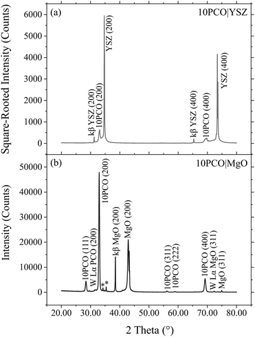 |
| | Fig. 2 25 °C X-Ray diffraction (XRD) survey scans of 10PCO|YSZ (top) and 10PCO|MgO (bottom) showing that the 10PCO had mainly a (100) preferred crystallographic orientation. Note, the asterisk denotes the position of a (400) YSZ diffraction peak caused by tungsten X-rays emitted from impurity tungsten that sublimated off the electron emitter tip and onto the Ni target within the XRD source. | |
As shown by the SEM cross-sections in Fig. S1 of the ESI,† all the thin films produced here were dense and had laterally-uniform thicknesses of 233 ± 8 nm, regardless of their substrate material.
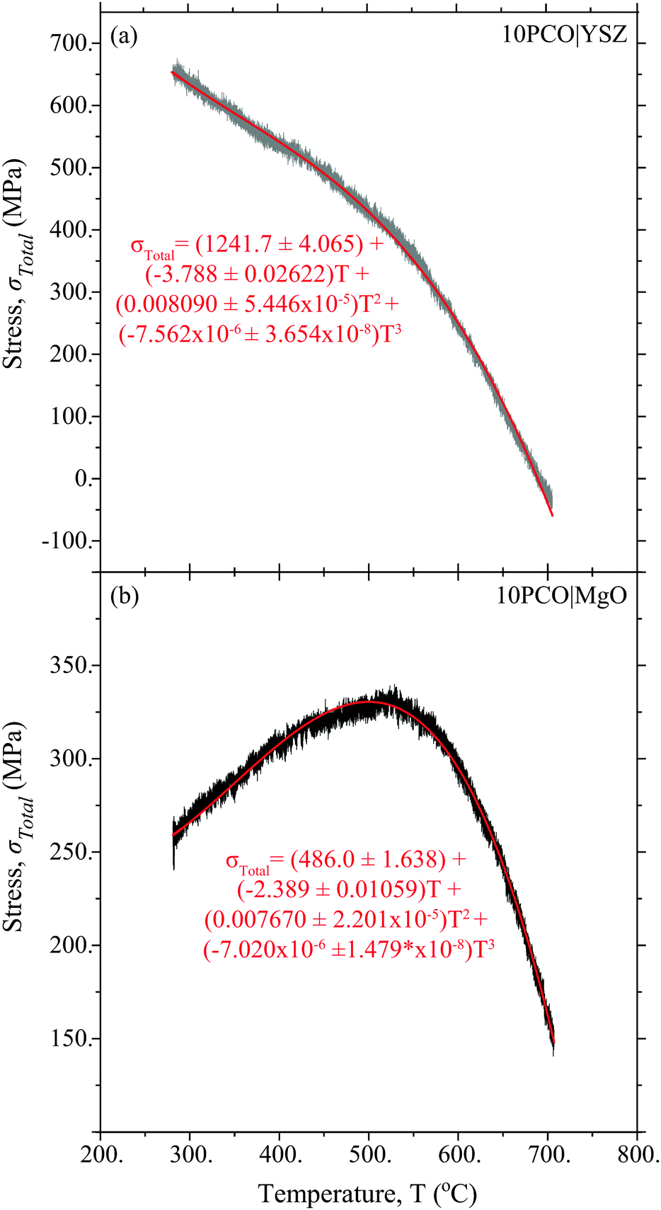
Fig. 3 shows the 10PCO|MgO and 10PCO|YSZ in-plane stress vs. temperature data used to calculate α, M, and E using the DS technique. As discussed in Ma and Nicholas,10 the evolution of these curve shapes vs. temperature were consistent with the anticipated thermal expansion coefficient differences between PCO, MgO and YSZ at various temperatures. As shown in the ESI† of Ma and Nicholas,10 this data was reproducible over multiple heating and cooling cycles, suggesting that all the samples remained in the linear elastic regime during testing.
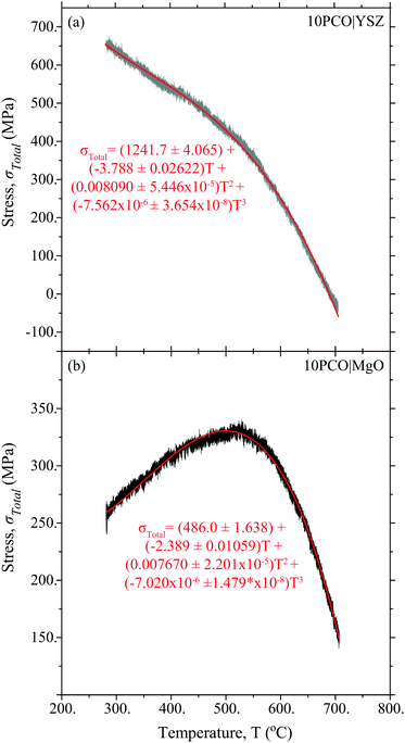 |
| | Fig. 3 Raw and fitted stress vs. temperature data used to determine α, M, and E via the DS technique. The plus or minus terms in the formulas denote the equations corresponding to plus or minus a standard deviation in the fitted data. | |
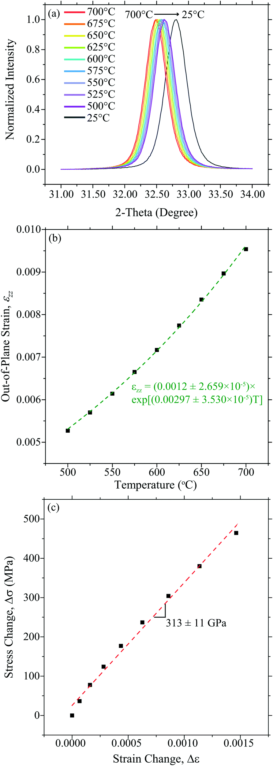
Similarly, Fig. 4 shows the 10PCO|YSZ temperature-dependent strain data used to calculate α, M, and E using the DC technique.
 |
| | Fig. 4 The (a) out-of-plane XRD-determined shift of the (200) 10PCO peak, (b) the corresponding total out-of-plane engineering strain, and corresponding fit, calculated from that shift (assuming an eqn (9) zero-strain state at 25 °C) used to obtain αfviaeqn (7), and (c) the comparison of the in-plane strain (calculated from that αfviaeqn (3)) vs. the in-plane stress (obtained via in situ 10PCO|YSZ wafer curvature measurements) used to determine M in the DC technique. | |
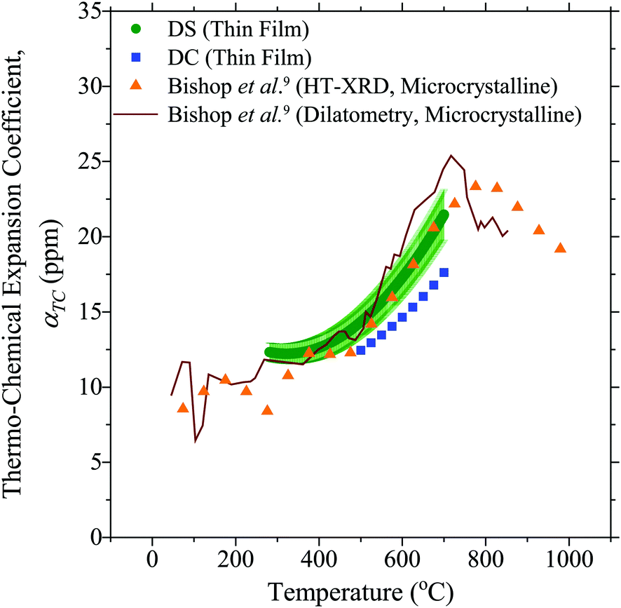
Fig. 5 compares the thermochemical expansion coefficients measured here, to those in the literature.9 Since the thermal expansion coefficients of cubic materials like 10PCO are isotropic within the lattice,38 a direct comparison between literature data and the values measured here was possible. Curiously, the thin film 10PCO α values obtained from the DS technique, which increased from ∼12.5 ppm at 500 °C to ∼17.5 ppm at 700 °C, agreed well with those obtained on bulk microcrystalline materials (via dilatometry and high temperature XRD),9 but were higher than the thin film 10PCO α values obtained from the DC technique. Although the exact reasons for this are unclear, multiple studies have suggested that the grain boundaries of ceria are easier to reduce than the lattice interior.39,40 Hence, the low angle grain boundaries/defective regions around the large amount of threading dislocations known to exist in YSZ supported PCO thin films17 (and suggested by the preferred orientation/epitaxy indicated by Fig. 2) may behave like they are in a lower pO2 portion of the ceria Brouwer diagram,41 and hence might be expected to possess a higher thermochemical expansion coefficient than the bulk. Since these defects are mainly oriented perpendicular to the plane of the film, this situation would violate the assumption of an isotropic α used in the DC technique. The increasing thermochemical expansion values that occur in 10PCO as the material is heated from 500 to 700 °C10 (as the material becomes more oxygen deficient; i.e. as it acts as if it's in a lower pO2 portion of the ceria Brouwer diagram) is consistent with higher Fig. 5α values for the DS compared to the DC technique. (Note, the ±8% measurement error bars around the DS α values, and the <1% measurement error bars around the DC α values are similar in size to those reported in other studies utilizing these techniques.16,42 That being said, the DC error bars may actually be larger than 1%, due to preferred orientation of the films shown in Fig. 2 violating the assumption in the DC technique that the αf in the plane of the film, and perpendicular to it, are equal).
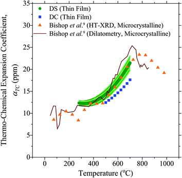 |
| | Fig. 5 The thermo-chemical expansion coefficient of 10PCO measured here, compared to the literature.9 Note, the estimated error bars on the DC data points are smaller than the symbol size, and HT-XRD denotes high temperature X-ray diffraction. | |
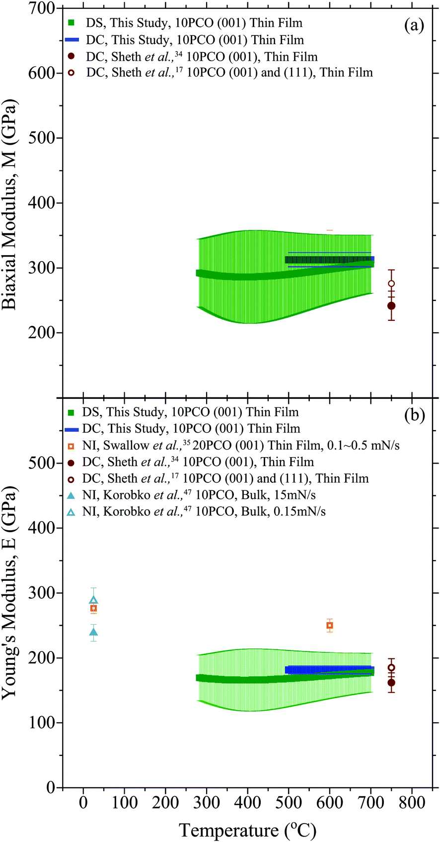
Fig. 6a compares the 10PCO biaxial moduli obtained here from the DS and the DC techniques with previous biaxial moduli values from the literature. For all the measurements here, the measured M values were roughly constant at ∼300 GPa from 500–700 °C, suggesting that the 10PCO elastic constants are largely insensitive to the ∼5% change in the 10PCO lattice oxygen stoichiometry known to occur in these films over this temperature range.10 This insensitivity to oxygen nonstoichiometry may also explain why the M values measured from the DS and DC techniques agreed so well with each other (since any local oxygen stoichiometry differences brought about by in-plane versus out-of-plane structural differences would have no effect).
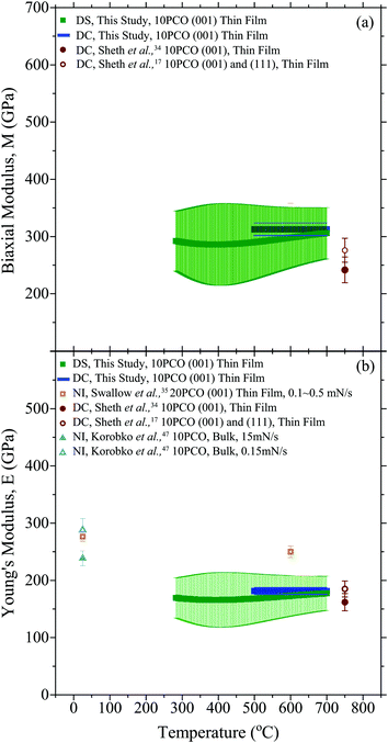 |
| | Fig. 6 The (a) biaxial modulus, and (b) Young's modulus of 10PCO measure here, compared to the literature.17,34,35,43 NI denotes values obtained from nano-indentation, while the other abbreviations have their previously defined meanings. Note, the estimated error bars on the DC data points are smaller than the symbol size. | |
Fig. 6b compares the 10PCO Young's moduli obtained here from the DS and the DC techniques with the literature.17,34,35,43 For all the measurements here, the DS and DC techniques yielded average (100) direction 10PCO values that were roughly constant at ∼175 GPa from 500–700 °C. It is important to note that even though they came from the same biaxial modulus, the ∼175 GPa DS-determined Young's modulus values here are more accurate than the ∼200 GPa DS-determined values from Ma and Nicholas,10 because a more correct Poisson ratio of 0.42 for (100)-oriented ceria (corresponding to the preferred film orientation shown in Fig. 2) was used to extract the Young's Modulus from the biaxial modulus here (viaeqn (2)), instead of the 0.33 average Poisson's ratio value for randomly-oriented polycrystalline used previously for PLD 10PCO thin films on YSZ and/or sapphire substrates.10,34,35 The Young's moduli measured here agreed well with the DC data reported by Sheth et al.17,34 but they did not agree with the nano-indentation data of either Swallow et al.35 or Korobko et al.,43 presumably due to the different 10PCO doping levels examined in Swallow et al.35 and/or the loading-rate-dependent E values obtained via nano-indentation43 as a result of the elastic dipole reorientation known to occur in ceria below ∼250 °C.18,44
Conclusions
This work demonstrated that similar thermochemical expansion coefficients, biaxial moduli, and Young's moduli values could be obtained using either (1) in situ stress vs. temperature measurements of (100)-oriented Pr0.1Ce0.9O1.95−x thin films on either YSZ or MgO single crystal substrates, or (2) combined in situ stress vs. temperature and in situ strain vs. temperature measurements on a single (100)-oriented Pr0.1Ce0.9O1.95−x thin film on YSZ. While they both had their limitations (the potentially-violated assumption of “identical substrates on different substrates” in the DS technique, the potentially-violated assumption of isotropic thermochemical expansion coefficients in the DC technique, etc.), both techniques indicated that in the (100) plane of Pr0.1Ce0.9O1.95−x from 500 to 700 °C, (1) the directionally-averaged thermo-chemical expansion coefficient increased from ∼12.5 to ∼17.5 ppm, (2) the biaxial modulus was roughly constant at ∼300 GPa, and (3) the directionally-averaged Young's modulus was roughly constant at ∼175 GPa. These high temperature materials properties could be useful for designing Solid Oxide Electrolysis Cells, Solid Oxide Fuel Cells, or other electrochemical devices utilizing high temperature Pr0.1Ce0.9O1.95−x thin films.
Conflicts of interest
There are no conflicts to declare.
Acknowledgements
This work was generously supported by the Department of Energy under Award Number DE-FE0023315. The microscopy work was conducted at the Michigan State Composites Center, which is supported by the NSF Major Instrumentation Program and Michigan State University. The authors would like to thank Dr Timothy Hogan and Mr Karl Dersch of Michigan State University for assistance with the thin film deposition. The authors would also like to thank Dr Alexandra Zevalkink, Dr Elias Garratt, and Mr Shengyuan Bai for assistance with the XRD measurements.
References
- A. Atkinson, S. A. Barnett, R. J. Gorte, J. T. S. Irvine, A. J. McEvoy, M. B. Mogensen, S. Singhal and J. Vohs, Nat. Mater., 2004, 3, 17–27 CrossRef CAS PubMed.
- M. Hecht, J. Hoffman, D. Rapp, J. McClean, J. SooHoo, R. Schaefer, A. Aboobaker, J. Mellstrom, J. Hartvigsen, F. Meyen, E. Hinterman, G. Voecks, A. Liu, M. Nasr, J. Lewis, J. Johnson, C. Guernsey, J. Swoboda, C. Eckert, C. Alcalde, M. Poirier, P. Khopkar, S. Elangovan, M. Madsen, P. Smith, C. Graves, G. Sanders, K. Araghi, M. D. Juarez, D. Larsen, J. Agui, A. Burns, K. Lackner, R. Nielsen, T. Pike, B. Tata, K. Wilson, T. Brown, T. Disarro, R. Morris, R. Steinkraus, R. Surampudi, T. Werne and A. Ponce, Space Sci. Rev., 2021, 217, 76 CrossRef.
- W. C. Chueh, C. Falter, M. Abbott, D. Scipio, P. Furler, S. M. Haile and A. Steinfeld, Science, 2010, 330, 1797–1801 CrossRef CAS PubMed.
- J. Kaspar, P. Fornasiero and M. Graziani, Catal. Today, 1999, 50, 285–298 CrossRef CAS.
- P. Jasinski, T. Suzuki and H. U. Anderson, Sens. Actuators, B, 2003, 95, 73–77 CrossRef CAS.
- A. Younis, D. Chu, X. Lin, J. Yi, F. Dang and S. Li, ACS Appl. Mater. Interfaces, 2013, 5, 2249–2254 CrossRef CAS PubMed.
- V. V. Kharton, A. V. Kovalevsky, A. P. Viskup, A. L. Shaula, F. M. Figueiredo, E. N. Naumovich and F. M. B. Marques, Solid State Ionics, 2003, 160, 247–258 CrossRef CAS.
- N. Özer, Sol. Energy Mater. Sol. Cells, 2001, 68, 391–400 CrossRef.
- S. R. Bishop, H. L. Tuller, Y. Kuru and B. Yildiz, J. Eur. Ceram. Soc., 2011, 31, 2351–2356 CrossRef CAS.
- Y. Ma and J. D. Nicholas, Phys. Chem. Chem. Phys., 2018, 20, 27350–27360 RSC.
- L. J. Gauckler, M. Gödickemeier and D. Schneider, J. Electroceram., 1997, 1, 165–172 CrossRef.
- P. S. Manning, J. D. Sirman and J. A. Kilner, Solid State Ionics, 1997, 93, 125–132 CrossRef.
- M. Kamiya, E. Shimada, Y. Ikuma, M. Komatsu and H. Haneda, J. Electrochem. Soc., 2000, 147, 1222–1227 CrossRef CAS.
- T. F. Retajczyk and A. K. Sinha, Appl. Phys. Lett., 1980, 36, 161–163 CrossRef CAS.
- M. M. De Lima, R. G. Lacerda, J. Vilcarromero and F. C. Marques, J. Appl. Phys., 1999, 86, 4936 CrossRef CAS.
- J. Thurn and M. P. Hughey, J. Appl. Phys., 2004, 95, 7892–7897 CrossRef CAS.
- J. Sheth, D. Chen, J. J. Kim, W. J. Bowman, P. A. Crozier, H. L. Tuller, S. T. Misture, S. Zdzieszynski, B. W. Sheldon and S. R. Bishop, Nanoscale, 2016, 8, 16499–16510 RSC.
- T. Das, J. D. Nicholas, B. W. Sheldon and Y. Qi, Phys. Chem. Chem. Phys., 2018, 20, 15293–15299 RSC.
- N. Savvides, A. Thorley, S. Gnanarajan and A. Katsaros, Thin Solid Films, 2001, 388, 177–182 CrossRef CAS.
- J. D. Nicholas, Extreme Mech. Lett., 2016, 9, 405–421 CrossRef.
-
L. B. Freund and S. Suresh, Thin Film Materials: Stress, Defect Formation and Surface Evolution, Cambridge University Press, New York, NY, 2003 Search PubMed.
- G. G. Stoney, Proc. R. Soc. London, Ser. A, 1909, 82, 172–175 CAS.
-
J. D. Nicholas, in Electro-Chemo-Mechanics of Solids, ed. S. Bishop, D. Marrocchelli, N. Perry and B. Sheldon, Springer, New York, 2017, ch. 5, pp. 103–136 DOI:10.1007/978-3-319-51407-9_5.
- D. G. Isaak, O. L. Anderson and T. Goto, Phys. Chem. Miner., 1989, 16, 704–713 CrossRef CAS.
- P. J. Botha, J. C. H. Chiang, J. D. Comins, P. M. Mjwara and P. E. Ngoepe, J. Appl. Phys., 1993, 73, 7268–7274 CrossRef CAS.
- S. V. Sinogeikin, D. L. Lakshtanov, J. D. Nicholas, J. M. Jackson and J. D. Bass, J. Eur. Ceram. Soc., 2005, 25, 1313–1324 CrossRef CAS.
- H. Hayashi, T. Saitou, N. Maruyama, H. Inaba, K. Kawamura and M. Mori, Solid State Ionics, 2005, 176, 613–619 CrossRef CAS.
- I. Suzuki, J. Phys. Earth, 1975, 23, 145–159 CrossRef.
- T. Kushi, K. Sato, A. Unemoto, S. Hashimoto, K. Amezawa and T. Kawada, J. Power Sources, 2011, 196, 7989–7993 CrossRef CAS.
- A. Nakajima, A. Yoshihara and M. Ishigame, Phys. Rev. B: Condens. Matter Mater. Phys., 1994, 50, 13297–13307 CrossRef CAS PubMed.
-
B. D. Cullity, Elements of X-Ray Diffraction, Addison-Wesley, New York, 2nd edn, 1978 Search PubMed.
- M. M. Hall, V. G. Veeraraghavan, H. Rubin and P. G. Winchell, J. Appl. Crystallogr., 1977, 10, 66–68 CrossRef.
- D. Chen, S. R. Bishop and H. L. Tuller, J. Electroceram., 2012, 28, 62–69 CrossRef CAS.
- J. Sheth, D. Chen, H. L. Tuller, S. T. Misture, S. R. Bishop and B. W. Sheldon, Phys. Chem. Chem. Phys., 2017, 19, 12206–12220 RSC.
- J. G. Swallow, J. J. Kim, M. Kabir, J. F. Smith, H. L. Tuller, S. R. Bishop and K. J. Van Vliet, Acta Mater., 2016, 105, 16–24 CrossRef CAS.
- D. Chen, S. R. Bishop and H. L. Tuller, Adv. Funct. Mater., 2013, 23, 2168–2174 CrossRef CAS.
- J. J. Kim, S. R. Bishop, N. J. Thompson, D. Chen and H. L. Tuller, Chem. Mater., 2014, 26, 1374–1379 CrossRef CAS.
-
J. F. Nye, Physical Properties of Crystals: Their Representation by Tensors and Matrices, Oxford University Press, New York, 1985 Search PubMed.
- B. W. Sheldon, S. Mandowara and J. Rankin, Solid State Ionics, 2013, 233, 38–46 CrossRef CAS.
- Y. M. Chiang, E. B. Lavik, I. Kosacki, H. L. Tuller and J. Y. Ying, Appl. Phys. Lett., 1996, 69, 185–187 CrossRef CAS.
- S. R. Bishop, T. S. Stefanik and H. L. Tuller, Phys. Chem. Chem. Phys., 2011, 13, 10165–10173 RSC.
- Y. Kuru, S. R. Bishop, J. J. Kim, B. Yildiz and H. L. Tuller, Solid State Ionics, 2011, 193, 1–4 CrossRef CAS.
- R. Korobko, S. K. Kim, S. Kim, S. R. Cohen, E. Wachtel and I. Lubomirsky, Adv. Funct. Mater., 2013, 23, 6076–6081 CrossRef CAS.
- A. Kossoy, Y. Feldman, R. Korobko, E. Wachtel, I. Lubomirsky and J. Maier, Adv. Funct. Mater., 2009, 19, 634–641 CrossRef CAS.
Footnote |
| † Electronic supplementary information (ESI) available. See DOI: 10.1039/d1ma00842k |
|
| This journal is © The Royal Society of Chemistry 2022 |
Click here to see how this site uses Cookies. View our privacy policy here. 
 Open Access Article
 This Open Access Article is licensed under a
  ,
Quan
Zhou
,
Quan
Zhou

 , the known substrate thermo-chemical expansion coefficient (αs), and a known/assumed vfvia the equation: