
 Open Access Article
 This Open Access Article is licensed under a Creative Commons Attribution-Non Commercial 3.0 Unported Licence
Facile growth of a Sb2Se3 nanorod array induced by a MoSe2 interlayer and its application in 3D p–n junction solar cells†
Si-Nae
Park‡
a,
Se-Yun
Kim‡
b,
Sang-Ju
Lee
ac,
Shi-Joon
Sung
 *ac,
Kee-Jeong
Yang
ac,
Jin-Kyu
Kang
ac and
Dae-Hwan
Kim
*ac
*ac,
Kee-Jeong
Yang
ac,
Jin-Kyu
Kang
ac and
Dae-Hwan
Kim
*ac
aResearch Center for Thin Film Solar Cells, Daegu-Gyeongbuk Institute of Science and Technology (DGIST), Daegu 42988, Republic of Korea. E-mail: sjsung@dgist.ac.kr; monolith@dgist.ac.kr
bDepartment of Materials Science and Engineering, Kyungnam University, Geyongsangnam-do 51767, Republic of Korea
cDivision of Energy Technology, Daegu-Gyeongbuk Institute of Science and Technology (DGIST), Daegu 42988, Republic of Korea
First published on 21st December 2021
Abstract
A uniformly grown Sb2Se3 nanorod array, with the introduction of a MoSe2 interlayer, obtained by a co-evaporation process and its application in three-dimensional (3D) p–n junction high-efficiency Sb2Se3 solar cells were investigated in this study. The MoSe2 interlayer played a crucial role as a seed layer for the preferential growth of Sb2Se3 crystals, which facilitated the formation of a Sb2Se3 nanorod array regardless of the process conditions. 3D p–n junction between the Sb2Se3 nanorod array and the CdS buffer layer improved the short-circuit current of Sb2Se3 solar cells due to improved carrier transportation from the Sb2Se3 absorber to the CdS buffer. The MoSe2 interlayer also improved the contact quality between the Sb2Se3 nanorod array and the Mo substrate by forming a quasi-ohmic contact, which resulted in a higher open-circuit voltage due to a reduced contact barrier and series resistance in Sb2Se3 solar cells. The crystal growth rate of Sb2Se3 was controlled by the source evaporation rate and substrate temperature to tune the final nanostructure and crystalline orientation of the co-evaporated Sb2Se3 nanorods array. 3D p–n junction solar cells based on an ordered and (hk1) preferentially oriented Sb2Se3 nanorod array showed a power conversion efficiency of 5.637%. Therefore, by including a MoSe2 interlayer, it is possible to achieve high-efficiency 3D p–n junction Sb2Se3 solar cells.
Introduction
Antimony selenide (Sb2Se3) is one of the most promising semiconductor materials for thin-film solar cells because of its outstanding optoelectronic properties. Additionally, it is a non-toxic, relatively low-cost material with high absorption coefficient and low processing temperature.1–6 Therefore, significant research has been conducted in the past decade to replace the conventional multinary compound semiconductors in thin-film solar cells for Sb2Se3.7–11 However, the best power conversion efficiency (PCE) reported so far for Sb2Se3 solar cells is approximately 10%,12 which is similar to those of thin-film solar cells made of conventional materials. In order to overcome the efficiency limitation of the Sb2Se3 solar cells, the application of three-dimensional (3D) nanostructured Sb2Se3 thin films for the formation of the 3D p–n junction solar cells could be one of the promising solutions.13–15Carrier transportation and p–n junction formation in Sb2Se3 solar cells are closely related to the Sb2Se3 nanostructure. Therefore, the latter is one of the critical factors determining the photovoltaic performance of Sb2Se3 solar cells. However, there is little study on the nanostructure control of the Sb2Se3 thin films for high efficiency solar cells. Li et al. improved the short-circuit current (JSC) of a solar cell using a 1000 nm-high Sb2Se3–nanorod array with superior light-harvesting capacity and reduced optical reflection.16 In our previous work, we investigated the evolution of Sb2Se3 nanorods by controlling the process temperature of co-evaporation and proposed the photovoltaic performance enhancement of Sb2Se3 solar cells based on 3D p–n junction formation.18 However, the temperature window for the formation of Sb2Se3 nanorods was narrow and the orientation of the Sb2Se3 nanorods was random. From these previously reported studies, it was found that the application of 3D nanostructured Sb2Se3 absorber layers would be very useful to overcome of the performance limitation of Sb2Se3 solar cells based on the 3D p–n junction solar cell concept. However, to the best of the authors’ knowledge, there is no detailed investigation of the nanostructure evolution of Sb2Se3 thin films reported in the literature.
The objective of this work was to study the evolution of a nanostructured Sb2Se3 thin film fabricated using a MoSe2 interlayer and the co-evaporation process. Additionally, a detailed investigation of the controlling factor to achieve fine-tuned Sb2Se3 nanorod arrays is presented in this work. In our work, we proposed the evolution of nanostructured Sb2Se3 thin films using a MoSe2 interlayer and detailed investigation on the control factor of the co-evaporation process for the fine-tuning of the Sb2Se3 nanorod array. By introducing a MoSe2 interlayer between the Mo substrate and Sb2Se3, it was possible to form uniformly ordered packed Sb2Se3 nanorod formation using co-evaporation of Sb2Se3 and Se sources. The MoSe2 interlayer has locally distributed dangling bonds, which play the role of nucleation seed for Sb2Se3 crystalline growth perpendicular to the Mo substrate. Because of the seeding effect of the MoSe2 interlayer, Sb2Se3 thin films deposited on the MoSe2 interlayer dominantly showed a uniformly ordered packed Sb2Se3 nanorod array. In addition, the formation of a quasi-ohmic contact between Sb2Se3 and MoSe2 was another improving point of open-circuit voltage (VOC) of Sb2Se3 solar cells compared with Sb2Se3 solar cells without the MoSe2 interlayer.
The nanostructure of the Sb2Se3 nanorod arrays on the MoSe2 interlayer was also sensitively affected by the conditions of the co-evaporation processes, such as the evaporation rate of sources and substrate temperature. The growth behavior of Sb2Se3 crystals during the co-evaporation process was closely related with the final nanostructure of Sb2Se3 nanorod array, which was the main factor that determines the short-circuit current (JSC) of Sb2Se3 solar cells. The crystalline orientation of co-evaporated Sb2Se3 thin films, which is a crucial factor for high efficiency Sb2Se3 solar cells, was also affected by the substrate temperature.18–25 After chemical bath deposition (CBD) of n-type CdS buffer layers on the Sb2Se3 nanorod array, the 3D p–n junction between Sb2Se3 and CdS was formed and the 3D p–n junction was effective for the enhancement of JSC. By introducing the MoSe2 interlayer, the growth of a uniformly ordered Sb2Se3 nanorod array and the quasi-ohmic contact between Sb2Se3 and MoSe2 were possible and 3D p–n junction Sb2Se3 solar cells with 5.637% efficiency was achieved.
Experimental
MoSe2 interlayer and Sb2Se3 thin-film preparation
The structure of the studied Sb2Se3 thin films consisted of a soda-lime glass (SLG) substrate and a 600 nm-thick Mo layer as the back-contact layer. Before deposition, the substrate was sequentially cleaned in an ultrasonic bath using acetone, methanol, and deionized water. The Mo layer was deposited on the SLG substrate via direct current (DC) magnetron sputtering using a Mo target with a purity of 99.99%.To form the MoSe2 interlayer on Mo substrates, the latter were treated in a tube furnace in a Se atmosphere. Vacuum (10−3 Torr) was applied to the furnace to remove moisture and impurities. Then, Ar gas was introduced into the furnace, allowing the pressure inside the furnace to reach the atmospheric pressure. The furnace was heated to 430 °C with Se pellets inside for 10 min and then annealed for 10 min. The MoSe2 layer obtained was approximately 100 nm-thick.
The Sb2Se3 thin films were prepared on bare Mo substrates or MoSe2/Mo substrates using a co-evaporator system using Sb2Se3 and Se sources. The substrate temperature was controlled in the range of 250–290 °C. The substrate was heated at 0.53 °C s−1 from room temperature (∼25 °C) to the desired temperature. The evaporation rate of Sb2Se3 and Se sources varied from 50–200 Å s−1. Sb2Se3 was deposited to obtain thin films (thickness: approximately 500 nm). After deposition, the samples were allowed to cool to room temperature naturally.
Solar cell fabrication
Chemical bath deposition (CBD) was used to cover the Sb2Se3 thin films obtained with a 50 nm-thick n-type cadmium sulfide (CdS) buffer layer, and radiofrequency (RF) sputtering was used to sequentially deposit a 50 nm-thick intrinsic ZnO window layer and a 300 nm-thick Al-doped ZnO (AZO) A transparent conducting oxide (TCO) layer was deposited on top of the buffer layer to fabricate the solar cells. Thermal evaporation was then used to deposit a 1 μm-thick Al collection grid on top of the device.Characterization of Sb2Se3 solar cells
The Sb2Se3 thin films were analyzed using various techniques to determine the influence of substrate temperature on the chemical composition and morphology of the films, and consequently, on the photovoltaic characteristics of the Sb2Se3 solar cells. The surface morphology and chemical composition of the Sb2Se3 thin films were observed using field emission scanning electron microscopy (FE-SEM, Hitachi, SU8020) and transmission electron microscopy (FE-TEM, Hitachi, HF-3300) with a focused ion beam (FIB) system (Hitachi, NB 5000). The crystalline structure of the Sb2Se3 thin films was determined using X-ray diffraction (XRD) analysis (Panalytical, Empyrean). The photovoltaic characteristics of the solar cells were characterized using a source meter (Keithley, 2400) unit and a solar simulator (Newport, 94022A) to simulate 1.5AM solar irradiation.Results and discussion
To obtain a controlled Sb2Se3 crystalline structure in Sb2Se3 solar cells, an MoSe2 interlayer between the Sb2Se3 absorber and the Mo substrate was adopted. Additionally, the MoSe2 interlayer between Sb2Se3 and the Mo substrate played an important role in the growth control of the Sb2Se3 crystalline structure. To investigate the role and effect of the MoSe2 interlayer on Sb2Se3 crystal growth, Sb2Se3 thin films were deposited on bare Mo substrates and MoSe2/Mo substrates using the co-evaporation process at different source evaporation rates (50–200 Å s−1). The source evaporation rate is closely related to the Sb2Se3 crystal growth mechanism. Fig. 1 shows the cross-sectional SEM images of Sb2Se3 thin films with different substrates and at different evaporation rates.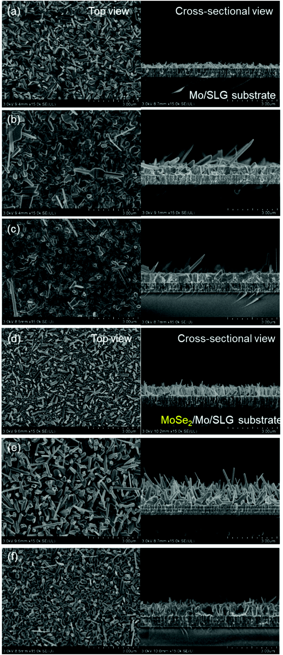 | ||
| Fig. 1 Top and cross-sectional SEM images of co-evaporated Sb2Se3 thin films on bare Mo substrates or MoSe2/Mo substrates at 290 °C and different source evaporation rates: (a), 50 Å s−1; (b), 100 Å s−1; and (c), 200 Å s−1 on bare Mo substrates; and (d), 50 Å s−1; (e), 100 Å s−1; and (f), 200 Å s−1 on MoSe2/Mo substrates. | ||
In the case of co-evaporated Sb2Se3 thin films on bare Mo substrates, thin films deposited at a slow source evaporation rate (50 Å s−1) showed a small and randomly oriented Sb2Se3 nanorod structure (Fig. 1a). However, as the source evaporation rate increased to 100 Å s−1, Sb2Se3 thin films showed a densely packed columnar structure with some long Sb2Se3 nanorods (Fig. 1b). At a source evaporation rate of 200 Å s−1, a flat Sb2Se3 thin-film structure comprising densely packed grains was observed (Fig. 1c). Generally, the nucleation rate is closely related to the evaporation rate.26 Thus, a easily formed continuous film under a high evaporation rate was expected. For film materials having an anisotropic crystal structure, such as Sb2Se3, rod-shaped film formation is highly probable when the evaporation rate is low. Under these conditions, the impingement rate of adatoms on the substrate decreases and their diffusion length may increase, causing the formation of a non-continuous film. Based on these results, authors believe that controlling the evaporation rate is critical to developing the Sb2Se3 rod array for 3D p–n junction solar cells.
Contrary to the co-evaporated Sb2Se3 thin films on Mo substrates, Sb2Se3 thin films prepared on MoSe2/Mo substrates showed a different nanostructure. All Sb2Se3 thin films on MoSe2/Mo substrates showed non-flat thin-film structures, regardless of the source evaporation rate. At an evaporation rate of 50 Å s−1, thin films showed a vertically oriented narrow Sb2Se3 nanorod array of length 500 nm (Fig. 1d). The diameter and length of the Sb2Se3 nanorods increased with increasing evaporation rate from 50 to 100 Å s−1 (Fig. 1e). At an evaporation rate of 200 Å s−1, the thin-film showed ordered arrays of thick Sb2Se3 nanorods with a diameter of 100 nm (Fig. 1f). Sb2Se3 thin films deposited on MoSe2 substrates showed a Sb2Se3 nanorod array structure regardless of the source evaporation rate. Additionally, the Sb2Se3 nanorod array nanostructure was tuned by varying the source evaporation rate. The formation of Sb2Se3 nanorod array on the MoSe2 interlayer might be attributed to different Sb2Se3 crystal growth mechanisms (Fig. 2). Moreover, the MoSe2 interlayer has unique anisotropic structural properties. For example, the (00l) plane of MoSe2 has no surface dangling bond, making the nucleation process difficult while facilitating the diffusion and desorption of adatoms on the (00l) plane of MoSe2. However, the nucleation process of Sb2Se3 could be easily formed on a plane having a high-dangling bond density, such as the one perpendicular to the (00l) plane. Therefore, the MoSe2 interlayer was expected to provide a selective nucleation site, facilitating the formation of the Sb2Se3 rod array on the MoSe2 interlayer. To investigate in detail the interface between Sb2Se3 and MoSe2, a high-angle annular detector dark-field scanning transmission electron microscopy (HADDF-STEM) image of the Sb2Se3/MoSe2/Mo sample was observed (Fig. S3, ESI†). The MoSe2 showed a two-dimensional crystal structure with weak van der Waals bonding forces and without dangling bonds in the c-plane of MoSe2. Overall, the layer structure was oriented perpendicular to the Mo substrate. Interestingly, in our case, the density of the MoSe2 interlayer bunch seemed relatively low. Thus, the orientation of the flexible bunch of the MoSe2 layer was not perfectly aligned. The exposed-MoSe2 layer on the surface consisted of a c-plane without dangling bonds and another plane with dangling bonds.
 | ||
| Fig. 2 Schematic diagram of the selective nucleation and growth mechanism of Sb2Se3 on the randomly grown MoSe2 interlayer; (a) low surface energy plane, (b) high surface energy plane, and (c) growth of Sb2Se3 nanorods on MoSe2 interlayer. | ||
To confirm the effect of the substrate type on the morphology of the co-evaporated Sb2Se3 thin films, we also deposited Sb2Se3 thin films on indium tin oxide (ITO) substrates using the same co-evaporation process. Unlike Mo substrates, all the co-evaporated Sb2Se3 thin films on ITO substrates showed a similar dense thin-film morphology, regardless of the source evaporation rate (Fig. S1, ESI†) and substrate temperature (Fig. S2, ESI†). These results show that the type of substrate had a significant effect on the formation of Sb2Se3 nanorods by the co-evaporation process.
To evaluate the photovoltaic characteristics of the co-evaporated Sb2Se3 thin films on different Mo and MoSe2/Mo substrates, three different Sb2Se3 solar cells with a planar device structure of SLG/Mo/MoSe2/Sb2Se3/CdS/i-ZnO/AZO/Al were fabricated. Fig. 3 shows the cross-sectional TEM and energy dispersive X-ray spectroscopy (EDS) mapping images of the Sb2Se3 solar cells fabricated at different source evaporation rates and with different substrates. The Sb2Se3 solar cells without the MoSe2 interlayer showed a planar structure (Fig. 3a and b), due to the flat Sb2Se3 thin-film structure shown in Fig. 1c. The CdS buffer, i-ZnO window, and AZO TCO layers were uniformly deposited on the flat Sb2Se3 absorber layer. However, the Sb2Se3 solar cells prepared on MoSe2/Mo substrates showed completely different nanostructures than those using the Mo substrate. The Sb2Se3 absorber layer showed a complex nanorod array, and the CdS buffer layer was deposited on the Sb2Se3 nanorods conformally. The ZnO and AZO layers deposited on the rough CdS/Sb2Se3 interface showed irregular nanostructures. At the bottom of the Sb2Se3 absorber layer, a uniformly formed MoSe2 interlayer was confirmed. Moreover, the source evaporation rate showed a considerable effect on the nanostructure of the Sb2Se3 absorber layer. The Sb2Se3 solar cells prepared using a 200 Å s−1 source evaporation rate on MoSe2/Mo substrates showed an irregular and agglomerated Sb2Se3 grain structure (Fig. 3c and d). However, when the evaporation rate decreased to 100 Å s−1, the Sb2Se3 absorber layer showed a more ordered and regular nanorod array (Fig. 3e and f). These different Sb2Se3 nanorod array structures observed according to the source evaporation rate were consistent with the SEM images (Fig. 1e and f).
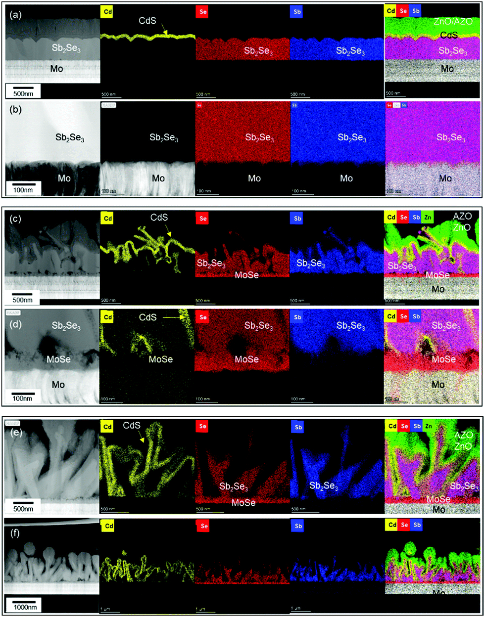 | ||
| Fig. 3 Cross-sectional TEM and EDS mapping images of Sb2Se3 solar cells fabricated with different source evaporation rates and at a temperature of 290 °C. (a) and (b), 200 Å s−1 on a Mo substrate; (c) and (d), 200 Å s−1 on a MoSe2/Mo substrate; and (e) and (f) 100 Å s−1 on a MoSe2/Mo substrate. | ||
Table 1 lists the photovoltaic properties of the Sb2Se3 solar cells with and without the MoSe2 interlayer. Despite the planar and uniform device structure of the Sb2Se3 solar cells without the MoSe2 interlayer, the solar cells with the MoSe2 interlayer showed a superior photovoltaic performance. The higher open-circuit voltage (VOC) showed by the Sb2Se3 solar cells with the MoSe2 interlayer might be attributed to the quasi-ohmic contact formation between Sb2Se3 and MoSe2. The quasi-ohmic contact formation of the MoSe2 interlayer is well known for copper indium gallium diselenide (CIGS) solar cells.27–31 This quasi-ohmic contact could reduce the contact barrier and series resistance of Sb2Se3 solar cell devices. The higher JSC could be related to the 3D p–n junction formation between the Sb2Se3 absorber and CdS buffer layers. Due to the 3D p–n junction structure, photo-generated carriers can easily escape into the CdS buffer layer. Thus, nanostructured Sb2Se3 solar cells show a higher JSC than flat thin-film Sb2Se3 solar cells. This superior photovoltaic performance was consistent with the results reported by Park et al. and was also attributed to the 3D p–n junction formation between the Sb2Se3 and CdS buffer layers.17 Between the two Sb2Se3 solar cells with a MoSe2 interlayer, the one fabricated at an evaporation rate of 100 Å s−1 showed higher JSC and fill factor (FF) than that at 200 Å s−1, which might be attributed to the more regular and ordered 3D p–n junction formation between Sb2Se3 and CdS.
| Substrate | Evaporation rate [Å s−1] | V OC [V] | J SC [mA cm−2] | FF [%] | Eff [%] | R s [Ω cm2] | R sh [Ω cm2] |
|---|---|---|---|---|---|---|---|
| Mo | 200 | 0.20297 | 8.4189 | 27.2369 | 0.465 | 18.105 | 26.703 |
| MoSe2/Mo | 200 | 0.43951 | 21.1832 | 36.0716 | 3.358 | 9.847 | 51.383 |
| MoSe2/Mo | 100 | 0.44999 | 23.6606 | 40.2727 | 4.288 | 8.488 | 70.319 |
A previous report showed that high substrate temperatures induce the evolution of Sb2Se3 nanorod arrays, demonstrating the close relationship between the nanostructure of co-evaporated Sb2Se3 thin films and substrate temperature.17 Therefore, we have tried to tune the nanostructure of co-evaporated Sb2Se3 thin films by controlling the substrate temperature at a source evaporation rate of 100 Å s−1 on MoSe2/Mo substrates. We also prepared co-evaporated Sb2Se3 thin films on bare Mo at 315 °C, which is the requirement for Sb2Se3 nanorod array formation on bare Mo substrates. Fig. 4 shows the top and cross-sectional SEM images of co-evaporated Sb2Se3 thin films at different substrate temperatures on bare Mo or MoSe2/Mo.
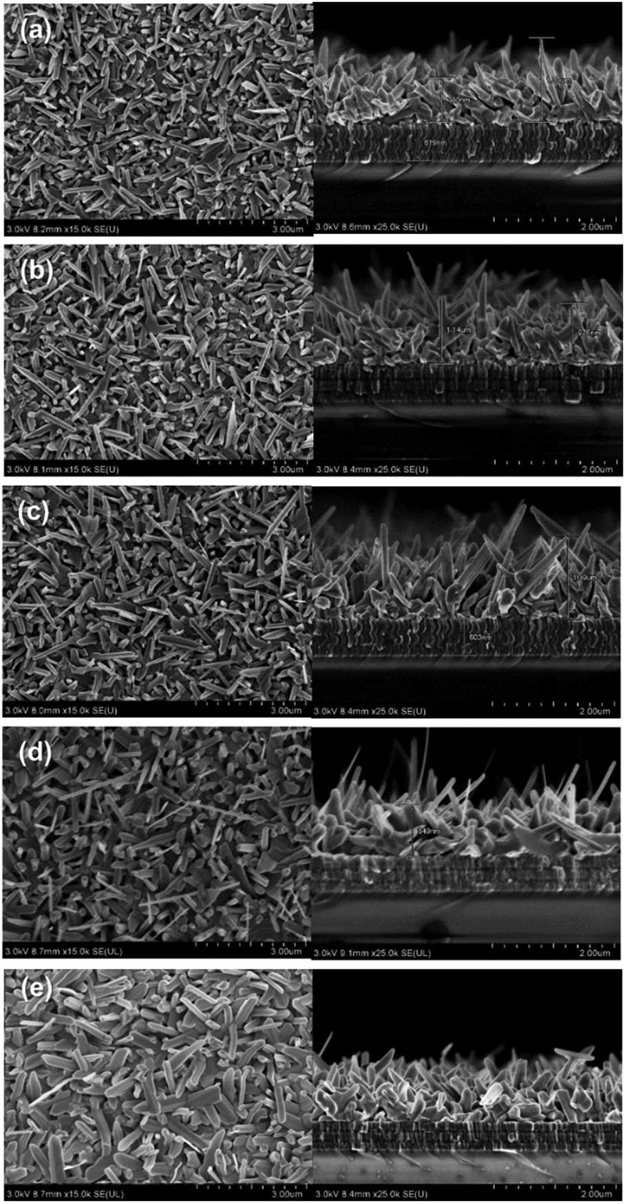 | ||
| Fig. 4 Top and cross-sectional SEM images of Sb2Se3 thin films at a source evaporation rate of 100 Å s−1 and different deposition temperatures: (a), 250; (b), 260; (c), 270; and (d), 290 °C using MoSe2/Mo substrates; and (e), 315 °C using a bare Mo substrate. | ||
The co-evaporated Sb2Se3 thin films on the MoSe2/Mo substrate did not show the abrupt morphology change, from the flat thin-film structure to a nanorod array, observed in our previous report on Mo substrates.17 Because the MoSe2 interlayer already easily induces the formation of the Sb2Se3 nanorod array, the substrate temperature showed little effect on the formation of the Sb2Se3 nanorod array. However, the detailed nanostructure of the Sb2Se3 nanorods was affected by the substrate temperature. As the substrate temperature decreased from 290 to 250 °C, the shape regularity and the degree of ordering of the Sb2Se3 nanorods improved. As the substrate temperature decreases, the Sb2Se3 nuclei density increases, suppressing the rapid growth of Sb2Se3 nanorods. Therefore, the growth of Sb2Se3 nanorods could be controlled effectively to form an ordered Sb2Se3 nanorod array by adjusting the substrate temperature on MoSe2/Mo. Moreover, using the MoSe2 interlayer, it was possible to control the nanostructure of co-evaporated Sb2Se3 thin films by varying both the evaporation rate and substrate temperature. Co-evaporated Sb2Se3 thin films on a bare Mo substrate at 315 °C also showed a similar Sb2Se3 nanorod structure to that on MoSe2/Mo substrates, which is consistent with the results from our previous work.17 The bare Mo substrate required a higher substrate temperature to form a similar Sb2Se3 nanorod array to the one obtained using MoSe2/Mo substrates and the co-evaporation process.
The crystalline orientation of Sb2Se3 thin films is well known to be crucial for determining the photovoltaic properties of Sb2Se3 solar cells due to the intrinsic one-dimensional ribbon structure of Sb2Se3.32–34 Therefore, the crystalline structure of co-evaporated Sb2Se3 thin films on MoSe2/Mo substrate at different substrate temperatures was analyzed by XRD analysis. All the co-evaporated Sb2Se3 thin films showed characteristic XRD peaks of Sb2Se3. However, the relative intensity of specific peaks corresponding to different crystalline orientations was different for each substrate temperature. Particularly, at 260 °C where the (020) and (120) peaks were not observed, and the intensity of the (211) and (221) peaks increased (Fig. 5a). To further investigate the crystalline orientation of the co-evaporated Sb2Se3 thin films, their texture coefficient was calculated.35–37 At 260 °C the texture coefficient of the (211) peak was remarkably higher than that at other substrate temperatures (Fig. 5b). Additionally, all other Sb2Se3 thin films showed relatively higher texture coefficients of (hk0) than those at 260 °C. The (hk1) preferential orientation of the Sb2Se3 thin film at a substrate temperature of 260 °C could help in improving the photovoltaic performance of Sb2Se3 solar cells.
 | ||
| Fig. 5 XRD peaks (a) and texture coefficient (b) of co-evaporated Sb2Se3 thin films at different substrate temperatures and at a source evaporation rate of 100 Å s−1. | ||
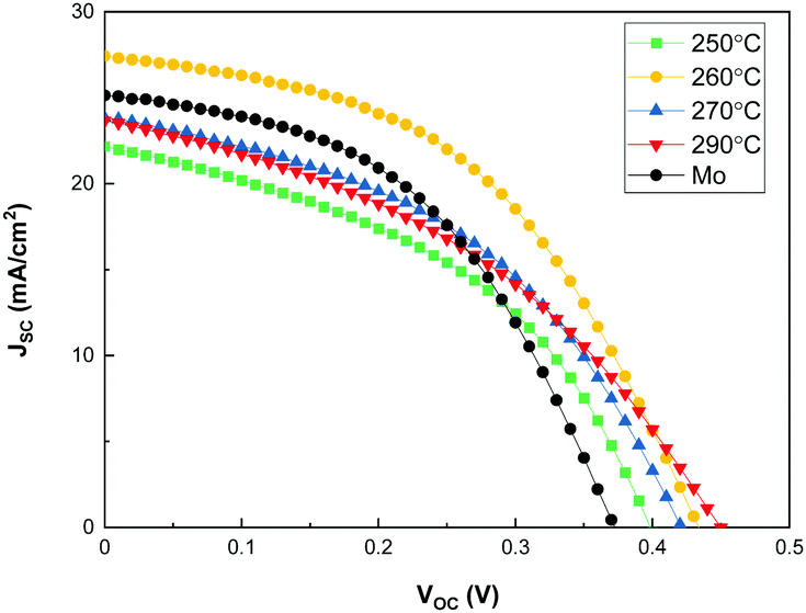
Sb2Se3 solar cells were fabricated at different substrate temperatures to investigate the effect of substrate temperature of co-evaporated Sb2Se3 thin films on their photovoltaic performance. Fig. 6 shows the I–V curves of the Sb2Se3 solar cells at a source evaporation rate of 100 Å s−1 and different substrate temperatures, and Table 2 lists the photovoltaic properties obtained for the Sb2Se3 solar cells. All the Sb2Se3 solar cells using the MoSe2 interlayer showed a VOC > 0.4 V, regardless of the substrate temperature. Because the MoSe2 interlayer already improved the VOC, the structural change in the Sb2Se3 nanorods had little effect on the VOC. The Sb2Se3 solar cell using a bare Mo substrate showed a slightly lower VOC (0.37 V) than that with MoSe2/Mo substrates. These results show that the introduction of the MoSe2 interlayer significantly improves the VOC of Sb2Se3 solar cells. The Sb2Se3 solar cell prepared at a substrate temperature of 260 °C showed the highest JSC. This might be attributed to the (hk1) preferential orientation of the Sb2Se3 absorber layer. Moreover, the ordered and regular Sb2Se3 nanorod array could help increase the area of the 3D p–n junction between Sb2Se3 and CdS, improving the JSC of the Sb2Se3 solar cells. By the way, it showed comparable JSC (25.138 mA cm−2) to those of the Sb2Se3 solar cell with MoSe2/Mo substrates because of the densely packed Sb2Se3 nanorod array. Interestingly, Sb2Se3 solar cells using a MoSe2/Mo substrate at 250, 270 and 290 °C showed a relatively smaller JSC than bare Mo substrate. The nanostructure changes of the co-evaporated Sb2Se3 nanorod array by temperature is remarkable (Fig. 4), which might be closely related to the JSC and FF of Sb2Se3 solar cells. At 250 °C, the width of Sb2Se3 nanorods is smaller than that at 260 °C, which is disadvantageous for sufficient light absorption. The length uniformity of Sb2Se3 nanorods at 270 and 290 °C is inferior compared to that at 260 °C. The irregular nanostructure of the Sb2Se3 nanorods induces insufficient light absorption and photo-generated carrier transportation. The thinner rods (250 °C) and increased empty space (270 °C) could deteriorate the FF by increasing the shunt paths too.
 | ||
| Fig. 6 I–V curves of Sb2Se3 solar cells at a source evaporation rate of 100 Å s−1 and different substrate temperatures: (a), 250; (b), 260; (c), 270; and (d), 290 °C using MoSe2/Mo and bare Mo substrates. | ||
| Substrate | Temperature [°C] | V OC [V] | J SC [mA cm−2] | FF [%] | Eff [%] | R s [Ω cm2] | R sh [Ω cm2] |
|---|---|---|---|---|---|---|---|
| MoSe2 | 250 | 0.40 | 22.167 | 43.99 | 3.886 | 5.48 | 67.59 |
| MoSe2 | 260 | 0.43 | 27.430 | 47.35 | 5.637 | 5.89 | 118.26 |
| MoSe2 | 270 | 0.42 | 23.834 | 44.47 | 4.464 | 6.04 | 80.89 |
| MoSe2 | 290 | 0.45 | 23.661 | 40.27 | 4.288 | 8.49 | 70.32 |
| Mo | 315 | 0.37 | 25.138 | 47.11 | 4.412 | 5.69 | 112.25 |
To investigate the correlation between the 3D p–n junction structure and the photovoltaic properties of Sb2Se3 solar cells, TEM analysis of the best Sb2Se3 solar cell, with the evaporation rate of 100 Å s−1 and the substrate temperature of 260 °C, was performed. Fig. 7 shows the TEM-EDS mapping images of the Sb2Se3 solar cell device with a nanorod array with a PCE of 5.637% (Table 2). The Sb2Se3 solar cell using a MoSe2/Mo substrate showed a 1.225% higher PCE than the one using a bare Mo substrate, which might be attributed to the improved VOC. A densely packed, uniformly distributed, Sb2Se3 nanorod array and the 3D p–n junction between CdS and Sb2Se3 nanorods were observed. These properties are advantageous for the enhancement of JSC. Additionally, the uniform MoSe2 interlayer between the Mo substrate and the Sb2Se3 nanorod array is beneficial for the formation of a quasi-ohmic contact between the layers.
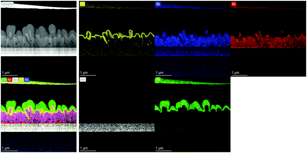 | ||
| Fig. 7 STEM-EDS mapping images of Sb2Se3 nanorod array solar cell with PCE of 5.637%. | ||
The results presented in this work reveal that the MoSe2 interlayer between a Mo substrate and a Sb2Se3 absorber layer improves the performance of Sb2Se3 solar cells in two relevant ways. First, the contact quality between Sb2Se3 and Mo layers improved due to quasi-ohmic contact formation, which was confirmed by the higher VOC values of Sb2Se3 solar cells using MoSe2/Mo substrates compared to those using a bare Mo substrate; second, a facile formation of the Sb2Se3 nanorod array and a lower substrate temperature were achieved using the co-evaporation process, which was followed by the 3D p–n junction Sb2Se3 solar cell fabrication. Moreover, the MoSe2 interlayer played a key role in improving the photovoltaic performance of the Sb2Se3 nanorod array solar cell by increasing both VOC and JSC. The quasi-ohmic contact caused by the MoSe2 interlayer effectively improved the contact quality between Sb2Se3 layers and Mo substrates. Moreover, the MoSe2 interlayer also played a critical role as a seed layer for the uniform growth of the Sb2Se3 nanorod array.
The Sb2Se3 solar cells prepared by co-evaporation at a source evaporation rate of 100 Å s−1 and substrate temperature of 260 °C on a MoSe2/Mo substrate were analyzed by an external certified laboratory to verify our PCE laboratory measurements. The certified J–V curve (Fig. 8a) and external quantum efficiency data (Fig. 8b) showed similar results (PCE of 5.484%) to our lab-scale photovoltaic measurements. We calculated integrated JSC from EQE data and compared with the JSC of J–V curve. The JSC from integrated EQE (25.89 mA cm−2) is similar to the JSC of the J–V curve (26.05 mA cm−2).
 | ||
| Fig. 8 Certified J–V curve (a) and external quantum efficiency (EQE) data (b) of Sb2Se3 solar cells at a substrate temperature of 260 °C and a source evaporation rate of 100 Å s−1 using a MoSe2/Mo substrate (Korea Institute of Energy Research, KIER). | ||
Conclusions
This work investigated the role of the MoSe2 interlayer on the growth of the Sb2Se3 nanorod array and the contact quality between Sb2Se3 thin films and Mo substrates. By introducing a MoSe2 interlayer between Sb2Se3 layers and Mo substrates, uniformly ordered densely packed Sb2Se3 nanorods were successfully prepared. The MoSe2 interlayer, with locally distributed high surface energy planes, played a crucial role as a seed layer for the preferential growth of Sb2Se3 crystals perpendicular to the substrate, which facilitated the formation of a Sb2Se3 nanorod array on the MoSe2 interlayer. The latter also significantly improved the photovoltaic performance of Sb2Se3 solar cell devices by forming a quasi-ohmic contact between Sb2Se3 absorber layers and Mo substrates, resulting in higher VOC and JSC. The nanostructure and crystalline orientation of the Sb2Se3 nanorods array were affected by the substrate temperature and the source evaporation rate during the co-evaporation process. 3D p–n junction solar cells based on an ordered and (hk1) preferentially oriented Sb2Se3 nanorods array showed a PCE of 5.637%.Conflicts of interest
There are no conflicts to declare.Acknowledgements
This work was supported by the DGIST R & D Programs of the Ministry of Science and ICT, Republic of Korea (21-CoE-ET-01, 21-ET-08). We thank Mr Eun and Mr Cheon at the Center for Core Research Facilities (CCRF) of DGIST for FIB sampling and STEM measurements.Notes and references
- Y. Zhou, M. Y. Leng, Z. Xia, J. Zhong, H. B. Song, X. S. Liu, B. Yang, J. P. Zhang, J. Chen, K. H. Zhou, J. B. Han, Y. B. Cheng and J. Tang, Adv. Energy Mater., 2014, 4, 1301846 CrossRef.
- G. X. Liang, Z. H. Zheng, P. Fan, J. T. Luo, J. G. Hu, X. H. Zhang, H. L. Ma, B. Fan, Z. K. Luo and D. P. Zhang, Sol. Energy Mater. Sol. Cells, 2018, 174, 263–270 CrossRef CAS.
- C. C. Yuan, L. J. Zhang, W. F. Liu and C. F. Zhu, Sol. Energy, 2016, 137, 256–260 CrossRef CAS.
- M. Birkett, W. M. Linhart, J. Stoner, L. J. Phillips, K. Durose, J. Alaria, J. D. Major, R. Kudrawiec and T. D. Veal, APL Mater., 2018, 6, 84901 CrossRef.
- X. M. Wang, R. F. Tang, C. Y. Wu, C. F. Zhu and T. Chen, J. Energy Chem., 2018, 27, 713–721 CrossRef.
- K. Shen, C. Z. Ou, T. L. Huang, H. B. Zhu, J. J. Li, Z. Q. Li and Y. Mai, Sol. Energy Mater. Sol. Cells, 2018, 186, 58–65 CrossRef CAS.
- S. Chen, T. Liu, Z. Zheng, M. Ishaq, G. Liang, P. Fan, T. Chen and J. Tang, J. Energy Chem., 2022, 67, 508–523 CrossRef.
- P. Fan, G. J. Chen, S. Chen, Z. H. Zheng, M. Azan, N. Ahmad, Z. H. Su, G. X. Liang, X. H. Zhang and Z. G. Chen, ACS Appl. Mater. Interfaces, 2021, 13, 46671–46680 CrossRef CAS PubMed.
- G. X. Liang, Y. D. Luo, S. Chen, R. Tang, Z. H. Zheng, X. J. Li, X. S. Liu, Y. K. Liu, Y. F. Li, X. Y. Chen, Z. H. Su and X. H. Zhang, Nano Energy, 2020, 73, 104806 CrossRef CAS.
- Y. D. Luo, R. Tang, S. Chen, J. G. Hu, Y. K. Liu, Y. F. Li, X. S. Liu, Z. H. Zheng, Z. H. Su, X. F. Ma, P. Fan, X. H. Zhang, H. L. Ma, Z. G. Chen and G. X. Liang, Chem. Eng. J., 2020, 393, 124599 CrossRef CAS.
- R. Tang, S. Z. H. Zheng, Z. H. Su, X. J. Li, Y. D. Wei, X. H. Zhang, Y. Q. Fu, J. T. Luo, P. Fan and G. X. Liang, Nano Energy, 2019, 64, 103929 CrossRef CAS.
- R. F. Tang, X. M. Wang, W. T. Lian, J. L. Huang, Q. Wei, M. L. Huang, Y. W. Yin, C. H. Jiang, S. F. Yang, G. C. Xing, S. Y. Chen, C. F. Zhu, X. J. Hao, M. A. Green and T. Chen, Nat. Energy, 2020, 5, 587–595 CrossRef CAS.
- P. V. Kamat, K. Tvrdy, D. R. Baker and J. G. Radich, Chem. Rev., 2010, 110, 6664–6688 CrossRef CAS PubMed.
- M. Yu, Y. Z. Long, B. Sun and Z. Y. Fan, Nanoscale, 2012, 4, 2783–2796 RSC.
- W. Yang, J. Ahn, Y. Oh, J. Tan, H. Lee, J. Park, H. C. Kwon, J. Kim, W. Jo, J. Kim and J. Moon, Adv. Energy Mater., 2018, 8, 1702888 CrossRef.
- Z. Q. Li, X. Y. Liang, G. Li, H. X. Liu, H. Y. Zhang, J. X. Guo, J. W. Chen, K. Shen, X. Y. San, W. Yu, R. E. I. Schropp and Y. H. Mai, Nat. Commun., 2019, 10, 125 CrossRef PubMed.
- S. N. Park, S. Y. Kim, S. J. Lee, S. J. Sung, K. J. Yang, J. K. Kang and D. H. Kim, J. Mater. Chem. A, 2019, 7, 25900–25907 RSC.
- Z. Li, X. Chen, H. Zhu, J. Chen, Y. Guo, C. Zhang, W. Zhang, X. Niu and Y. Mai, Sol. Energy Mater. Sol. Cells, 2017, 161, 190–196 CrossRef CAS.
- Y. H. Kwon, Y. B. Kim, M. Jeong, H. W. Do, H. K. Cho and J. Y. Lee, Sol. Energy Mater. Sol. Cells, 2017, 172, 11–17 CrossRef CAS.
- L. Wang, D. B. Li, K. H. Li, C. Chen, H. X. Deng, L. Gao, Y. Zhao, F. Jiang, L. Y. Li, F. Huang, Y. S. He, H. S. Song, G. D. Niu and J. Tang, Nat. Energy, 2017, 2, 17046 CrossRef CAS.
- C. Chen, L. Wang, L. Gao, D. Nam, D. B. Li, K. H. Li, Y. Zhao, C. Ge, H. Cheong, H. Liu, H. S. Song and J. Tang, ACS Energy Lett., 2017, 2, 2125–2132 CrossRef CAS.
- O. S. Hutter, L. J. Phillips, K. Durose and J. D. Major, Sol. Energy Mater. Sol. Cells, 2018, 188, 177–181 CrossRef CAS.
- C. Chen, K. H. Li, S. Y. Chen, L. Wang, S. C. Lu, Y. H. Liu, D. B. Li, H. S. Song and J. Tang, ACS Energy Lett., 2018, 3, 2335–2341 CrossRef CAS.
- X. X. Wen, C. Chen, S. C. Lu, K. H. Li, R. Kondrotas, Y. Zhao, W. H. Chen, L. Gao, C. Wang, J. Zhang, G. D. Niu and J. Tang, Nat. Commun., 2018, 9, 2179 CrossRef PubMed.
- K. H. Li, S. Y. Wang, C. Chen, R. Kondrotas, M. C. Hu, S. C. Lu, C. Wang, W. Chen and J. Tang, J. Mater. Chem. A, 2019, 7, 9665–9672 RSC.
- M. Ohring, in Materials Science of Thin Films, ed. M. Ohring, Academic Press, San Diego, 2nd edn, 2002, pp. 357–415 DOI:10.1016/B978-012524975-1/50010-0.
- H.-y. Sun, P.-h. Li, Y.-m. Xue, Z.-x. Qiao and L. Sai, Optoelectron. Lett., 2019, 15, 428–434 CrossRef.
- L. Assmann, J. C. Bernede, A. Drici, C. Amory, E. Halgand and M. Morsli, Appl. Surf. Sci., 2005, 246, 159–166 CrossRef CAS.
- N. Kohara, S. Nishiwaki, Y. Hashimoto, T. Negami and T. Wada, Sol. Energy Mater. Sol. Cells, 2001, 67, 209–215 CrossRef CAS.
- J. Chantana, T. Kato, H. Sugimoto and T. Minemoto, Appl. Phys. Lett., 2018, 112, 151601 CrossRef.
- S. Nishiwaki, N. Kohara, T. Negami and T. Wada, Jpn. J. Appl. Phys., 1998, 37, L71–L73 CrossRef CAS.
- Y. Zhou, L. Wang, S. Y. Chen, S. K. Qin, X. S. Liu, J. Chen, D. J. Xue, M. Luo, Y. Z. Cao, Y. B. Cheng, E. H. Sargent and J. Tang, Nat. Photonics, 2015, 9, 409–415 CrossRef CAS.
- Z. Q. Li, H. B. Zhu, Y. T. Guo, X. N. Niu, X. Chen, C. Zhang, W. Zhang, X. Y. Liang, D. Zhou, J. W. Chen and Y. H. Mai, Appl. Phys. Express, 2016, 9, 052302 CrossRef.
- X. S. Liu, J. Chen, M. Luo, M. Y. Leng, Z. Xia, Y. Zhou, S. K. Qin, D. J. Xue, L. Lv, H. Huang, D. M. Niu and J. Tang, ACS Appl. Mater. Interfaces, 2014, 6, 10687–10695 CrossRef CAS PubMed.
- S. Dias, B. Murali and S. B. Krupanidhi, Sol. Energy Mater. Sol. Cells, 2015, 143, 152–158 CrossRef CAS.
- S. Karim, M. E. Toimil-Molares, F. Maurer, G. Miehe, W. Ensinger, J. Liu, T. W. Cornelius and R. Neumann, Appl. Phys. A: Mater. Sci. Process., 2006, 84, 403–407 CrossRef CAS.
- Y. Q. Wang, W. Tang and L. Zhang, J. Mater. Sci. Technol., 2015, 31, 175–181 CrossRef CAS.
Footnotes |
| † Electronic supplementary information (ESI) available. See DOI: 10.1039/d1ma00804h |
| ‡ These authors contributed equally to this paper. |
| This journal is © The Royal Society of Chemistry 2022 |