
High-temperature polyimide dielectric materials for energy storage: theory, design, preparation and properties
Xue-Jie
Liu
a,
Ming-Sheng
Zheng
 *a,
George
Chen
b,
Zhi-Min
Dang
*c and
Jun-Wei
Zha
*ad
*a,
George
Chen
b,
Zhi-Min
Dang
*c and
Jun-Wei
Zha
*ad
aSchool of Chemistry and Biological Engineering, University of Science & Technology Beijing, Beijing 100083, P. R. China. E-mail: zhengms@ustb.edu.cn; zhajw@ustb.edu.cn
bDepartment of Electronics and Computer Science, University of Southampton, Southampton SO17 1BJ, UK
cState Key Laboratory of Power System, Department of Electrical Engineering, Tsinghua University, Beijing 100084, P. R. China. E-mail: Dangzm@tsinghua.edu.cn
dBeijing Advanced Innovation Center for Materials Genome Engineering, University of Science & Technology Beijing, Beijing 100083, P. R. China
First published on 20th November 2021
Abstract
Dielectric capacitors with a high operating temperature applied in electric vehicles, aerospace and underground exploration require dielectric materials with high temperature resistance and high energy density. Polyimide (PI) turns out to be a potential dielectric material for capacitor applications at high temperatures. In this review, the key parameters related to high temperature resistance and energy storage characteristics were introduced and recent developments in all-organic PI dielectrics and PI-matrix dielectric nanocomposites were discussed. Synthetic strategies for new functional PI via modification at the molecular level together with the design engineering of nanofillers and multilayer structures of PIs were also analysed. Finally, a systematic summary of the current challenges and future developments for capacitor materials used at high temperatures were presented.
 Xue-Jie Liu | Xue-Jie Liu is currently a PhD student at the University of Science and Technology Beijing under the supervision of Prof. Jun-Wei Zha. Her research interest is dielectric energy storage materials at high temperatures. |
 Jun-Wei Zha | Jun-Wei Zha received his PhD degree from the Beijing University of Chemical Engineering in 2010. He did his Joint-PhD in Electrical Power Engineering at University of Southampton from 2009 to 2010. He worked as a senior associate researcher and as a “Hong Kong Scholar” at City University of Hong Kong from 2013 to 2016. Now he is currently a Professor at the University of Science and Technology Beijing. His research interests are focussed on dielectric energy storage materials, thermal management in nanodielectrics and smart nanodielectrics, etc. He also serves as the subject editor of IET Nanodielectrics, youth editorial board member of Energy & Environmental Materials, etc. He is currently a member of IEEE/DEIS Technical Committee on Nanodielectrics and CIGRE WG D1-73. He has authored and co-authored over 170 papers in refereed journals, conference proceeding papers and 17 patents. He also has co-authored four English books and a Chinese Book. |
Broader contextTo meet the demands of energy storage for advanced electronics and electrical systems in a severe environment, dielectric materials with high thermotolerance are eagerly required to prepare capacitors. Polyimide (PI) has attracted lots of attention because of its high breakdown strength, excellent heat-resistance, simple synthesis process and easy designability of its molecular structure, which make it a great potential high-temperature dielectric material. Depending on the different applications, reactive monomers can be selected to provide groups with special functions (e.g. low dielectric loss). Various nanofillers were also used to improve the dielectric properties of PI, together with the design engineering of nanofillers and multilayer structures in the PI matrix. Herein, recent progress in all-organic PI dielectrics and PI nanocomposite dielectrics are discussed. The technological challenges and future developments for high temperature capacitor materials are analysed. This review will provide directions for the design and practical application of high-temperature energy storage materials for dielectric capacitors. |
1. Introduction
Dielectric materials are well known as the key component of dielectric capacitors. Compared with supercapacitors and lithium-ion batteries, dielectric capacitors store and release energy through local dipole cyclization, which enables rapid charge and discharge rates (high power density).1,2 Biaxially oriented polypropylene (BOPP) films have been widely used as dielectric films in capacitors. However, the maximum operating temperature of BOPP is lower than 105 °C due to the inferior melting point (∼165 °C). In addition, the dielectric loss (tan![[thin space (1/6-em)]](https://www.rsc.org/images/entities/char_2009.gif) δ) increases sharply and the charge–discharge efficiency (η) decreases accordingly above 80 °C.3–5 However, the maximum operating temperature of other capacitor films such as poly(ethylene-terephthalate) (PET), polycarbonate (PC) and polystyrene (PS), etc. are also limited to 125 °C.6 Therefore, no commercial capacitor films can meet the growing demand for high temperature (>125 °C) applications. As a result, to meet the demands of energy storage under high temperature conditions, extra cooling systems are required to maintain a low operating temperature of BOPP film capacitors, which led to low energy utilization efficiency, large weight/volume of the power system and high costs of production and operation.7 To achieve better performances at high operating temperatures, capacitors require higher energy density and more excellent temperature resistance.8
δ) increases sharply and the charge–discharge efficiency (η) decreases accordingly above 80 °C.3–5 However, the maximum operating temperature of other capacitor films such as poly(ethylene-terephthalate) (PET), polycarbonate (PC) and polystyrene (PS), etc. are also limited to 125 °C.6 Therefore, no commercial capacitor films can meet the growing demand for high temperature (>125 °C) applications. As a result, to meet the demands of energy storage under high temperature conditions, extra cooling systems are required to maintain a low operating temperature of BOPP film capacitors, which led to low energy utilization efficiency, large weight/volume of the power system and high costs of production and operation.7 To achieve better performances at high operating temperatures, capacitors require higher energy density and more excellent temperature resistance.8
Many dielectric materials have been developed for high temperature capacitor applications, but each has its limitations. Ceramic film capacitors have some of the smallest specific volumes and are particularly suitable for microelectronic systems, mobile platforms and miniaturized power devices.9 Generally, ceramics could endure high temperatures and show a high dielectric permittivity (εr), but their low breakdown strength (Eb) and poor flexibility limit their applications in the energy storage field.3 Dielectric polymers have been the preferred materials for capacitors due to their excellent electrical properties and the ease of customizing continuous large-area films with micron thickness.10 Various polymer dielectrics that are stable at high temperatures have been developed such as polyetheretherketone (PEEK), fluorene polyester (FPE) and polyimide (PI), which exhibit higher working temperatures (>125 °C) as shown in Table 1. Most high-temperature polymers had a high degree of aromaticity or fused-ring heterocyclic structures, and the presence of thermally stable rigid imide rings was one of the factors in the selection of PI as a candidate for a high-temperature dielectric material.11,12 Ma et al. used high-throughput density functional theory (DFT) to identify polymers that have the potential to be applied to capacitors. Among 267 polymers with unique and reasonable structures, PIs were selected for further research because of the high dielectric permittivity and wide band gap. In addition to the advantages of good flexibility and ease of mass preparation commonly found in polymers, the synthesis of PI offered excellent discretion in the fabrication process. Depending on the application, reactive monomers could be selected to provide groups with special functions (e.g. high thermal stability and low tanδ) during the preparation of PIs. Thus, the εr of PI (εr = 3–5) was promoted by rational design of molecular structures.13–16 Moreover, the development of multiphase materials based on PI is a promising method. For example, the dielectric properties of PI can be improved by introducing ceramic nanofillers (e.g. Al2O3,17,18 TiO2,19–23 CaCu3Ti4O12,24–27 and BaTiO328–31) and conductive nanofillers (e.g. graphene32,33 and carbon nanotubes (CNTs)34–36).
| Polymer | PC | PEEK | PEI | FPE | PI |
|---|---|---|---|---|---|
| U e (J cm−3) | ∼0.85 | ∼0.53 | ∼1.1 | ∼0.08 | ∼0.18 |
| Maximum operating temperature (°C) | 150 | 150 | 200 | 250 | 250 |
There are many reviews for film materials with high energy density at normal temperature for capacitors such as ceramic dielectrics,9,37 polymer dielectrics38,39 and nanocomposite dielectrics.2,10,40–46 Similarly, reviews of high-temperature capacitors are also available.3,8,11,47–49 However, publications concerning the use of PI for energy storage applications at elevated temperatures are not widely available. Enhancement in the properties of PIs are expected to lead to their applications in various fields requiring high-temperature energy storage, such as oil exploration, power grids, electric vehicles, aircraft, wind turbine generators, electronic circuits, etc., as shown in Fig. 1. The factors affecting the high-temperature energy storage properties of dielectric polymers including thermosetting aromatic polyimides and thermoplastic aromatic polyimides (such as polyetherimide, PEI) and their nanocomposites were analysed. In addition, the microstructure and interface properties of these materials, and the internal relationship between these factors and high-temperature dielectric properties were also explored. This review will provide meaningful guidance to the molecular and structure design, preparation process and practical use of PI capacitor materials for high temperature applications.
 | ||
| Fig. 1 Structures and future applications of the PI-matrix for dielectric capacitors. | ||
2. Basic parameters of high temperature capacitor materials
2.1 Energy storage performance
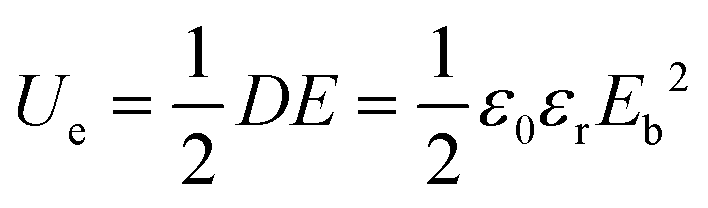
Generally, the energy storage density (U) of the dielectric capacitor can be given by eqn (1):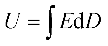 | (1) |
 | (2) |
| D = ε0εrE | (3) |
 | (4) |
![[thin space (1/6-em)]](https://www.rsc.org/images/entities/b_char_2009.gif) δ).
Dielectric properties are related to the polarization mechanism. The principle of energy storage and release arises from the polarization and depolarization process within the dielectric materials. Polarization (P) is defined as the total dipole moment in a dielectric per unit volume and is related to εr under a homogeneous applied field, which is shown as follows:41
δ).
Dielectric properties are related to the polarization mechanism. The principle of energy storage and release arises from the polarization and depolarization process within the dielectric materials. Polarization (P) is defined as the total dipole moment in a dielectric per unit volume and is related to εr under a homogeneous applied field, which is shown as follows:41| P = (εr − 1)ε0E | (5) |
 | ||
| Fig. 2 Four types of polarizations and their frequency dependencies: interfacial polarization, dipolar polarization, ionic polarization and electronic polarization. | ||
The positive and negative charge centers of the atom coincide in the absence of an external electric field. The displacement of the electron distribution in the presence of an applied electric field induces a dipole moment referred to as electronic polarization. The dipole moments of electronic polarization are very small, which occurs in all dielectrics.
The dipole moments generated by cations and anions in materials are neutralized in the absence of an external electric field. When an external electric field is applied, the anions and cations move in opposite directions resulting in polarization, referred to as ionic polarization. The dipole moments of ionic polarization are larger, which can give the material a higher εr. This polarization is common in ceramic materials such as barium titanate (BaTiO3).
Dipolar polarization results from molecules or molecular chains, which usually own inherent dipole moments. When there is no applied electric field, these dipole moments are randomly oriented. When an external electric field is applied, the molecules or molecular chains tend to distribute parallel to the direction of the electric field, thereby exhibiting macroscopic polarization. For polymers, the dipolar polarization depends on the presence of polar groups and the geometry of the polymer chains.41
Interfacial polarization is mainly related to the differences in the electrical characteristics of the constituent phases. When there is no external electric field, space charges distribute uniformly exhibiting non-polarization, while space charges accumulate under an applied electric field at the interface resulting in interfacial polarization.
PI has high electron mobility arising from the conjugated system of benzene rings and the lone pairs of electrons on the O and N of the imide rings, which will lead to the generation of electron polarization. However, the εr of PI is mainly contributed by dipolar polarization of their polar groups. Tong et al. analysed the εr of PIs with different structures as a function of temperature. As the operating temperature increases, only a slight change in the εr of PI is observed.50,51 Moreover, it should be noted that the high glass transition temperature (Tg) of PIs (usually higher than 200 °C) restricts the movement of the molecular chains, which endows PIs with high thermal stability dielectric characteristics in a wide temperature range.
The tanδ is a measure of the rate of energy loss during polarization and depolarization of dielectric materials.47 The tanδ mainly comes from polarization and electrical conduction. As shown in Fig. 2, electronic polarization and ionic polarization generally depend on the band gap of the polymer, and their loss peaks occur in the high frequency range (infrared and UV light levels).41 Dipolar polarization loss is seen at lower frequencies (radio level), and the loss peak of interfacial polarization occurs in the lowest frequency range (power level). PI is a linear dielectric with a low tanδ. However, the promotion strategies of εr usually leads to a higher tanδ. Thus, systematic consideration of the molecular/structure design according to the polarization mechanisms is necessary to improve the dielectric loss of PIs.
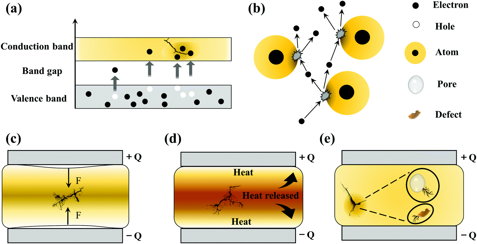
An ideal dielectric material under an electric field should exhibit high insulation and low conductivity. However, due to the combined effect of multiple conduction mechanisms, the current through the dielectric layer becomes larger when a stronger electric field is applied. According to the source of current, the conduction mechanism of the dielectrics can be divided into two types.52 The conduction mechanisms that depend on the electrical properties at the electrode-dielectric contact are called the electrode-limited conduction mechanisms, including Schottky emission, Fowler–Nordheim tunneling, direct tunneling, and thermionic-field emission. The bulk-limited conduction mechanisms only depend on the properties of the dielectric itself, including Poole–Frenkel emission, hopping conduction, ohmic conduction, space-charge-limited conduction, ionic conduction, etc.
Schottky emission, Poole–Frenkel emission and hopping conduction play a dominant role under high temperature conditions. As shown in Fig. 3(a), the Schottky emission describes the mechanism by which electrons in metal electrodes obtain sufficient energy from thermal activation to overcome the energy barrier at the metal/dielectric interface and be injected into the dielectrics to participate in the formation of conduction current. Poole–Frenkel (P–F) emission is sometimes called internal Schottky emission, that is, the thermally excited electrons can be emitted from the trap into the conduction band of the dielectrics as shown in Fig. 3(b). The Coulomb potential energy of the electron in the trapping center can be reduced by the applied electric field. The reduction in potential energy will increase the possibility of electrons being thermally excited out of the trap and entering the conduction band of the dielectrics. Hopping conduction is the tunneling effect in which electrons trapped in a dielectric film “hop” from one trap site to another as shown in Fig. 3(c). The P–F emission corresponds to the thermionic effect, and hopping conduction corresponds to the tunneling effect. Through the thermionic mechanism, carriers can overcome the trap barrier in P–F emission. In hopping conduction, even if the carrier energy is lower than the maximum energy of the barrier between the two trapping sites, carriers can still transit using the tunneling mechanism.
 | ||
| Fig. 3 Schematic energy band diagram of (a) Schottky emission, (b) Poole–Frenkel emission, and (c) hopping conduction in dielectrics (qΦB is the barrier height, Ec is the conduction band, Ev is the valence band and EF is the Fermi level). | ||
When the temperature is higher than a certain threshold, the continuously increasing temperature will cause the internal current of the polymer dielectrics to increase exponentially.53 It can be said that high temperatures have a significant destructive effect on dielectrics. The conduction loss in the dielectrics can be effectively suppressed by taking appropriate measures, such as the increase of the potential barrier at the electrode/dielectric to inhibit charge injection, the introduction of deep traps inside the dielectrics to reduce carrier mobility and the reduction of internal defects in the dielectrics.
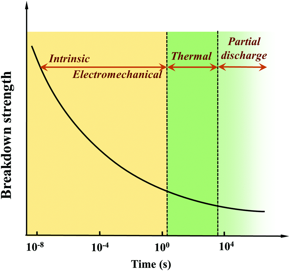 | ||
| Fig. 4 Breakdown mechanisms and Eb as a function of time after the application of a voltage.37 | ||
Intrinsic Eb can be defined as the highest breakdown value of a pure and homogeneous material where the measurement conditions are accurately controlled. Thus, the intrinsic Eb is an ideal value. There are two main types of intrinsic breakdown mechanisms, i.e. tunnel breakdown and avalanche breakdown. As shown in Fig. 5(a), electrons in the dielectrics can obtain enough energy from the electric field to cross the forbidden energy gap between the valence band and the conduction band. As more electrons accumulate in the conduction band, tunnel breakdown is achieved. The tunnel breakdown is related to the band gap of the dielectrics. It increases rapidly with the increase of the electric field, which will inevitably cause the dielectrics to lose the insulating properties. Electrons within dielectrics obtain energy from the electric field and collide with atoms. When the collision energy obtained by the atom exceeds the ionization potential, an electron is liberated (Fig. 5(b)). The collision ionization process proceeds as a chain reaction causing the number of electrons to increase sharply, resulting in an electron avalanche.37 The avalanche breakdown shows a high temperature dependence.
 | ||
| Fig. 5 Different types of breakdown mechanisms after the application of electric fields: (a) electronic breakdown, (b) avalanche breakdown, (c) electromechanical breakdown, (d) thermal breakdown, and (e) partial discharge breakdown. | ||
Electromechanical breakdown generally occurs in solid dielectrics with a low elastic modulus and easy mechanical deformation. Charges are induced on the surface of the dielectrics at high electric fields, and the electrostatic attraction of these charges causes compressive forces in Fig. 5(c). Electromechanical breakdown occurs if the forces exceed the mechanical compressive strength of the dielectrics.37
Thermal breakdown originates from the internal thermal instability of the dielectrics. Under the action of a high electric field, tanδ can cause energy dissipation to be consumed as heat, which increases the temperature of the dielectrics. The enhanced temperature increases the conductivity of the dielectrics exponentially, and the resulting higher conductivity loss will bring more heat. Thermal breakdown may occur when the rate of heat generation exceeds the rate of heat dissipation, as shown in Fig. 5(d). Thermal breakdown is related to the characteristics of the dielectrics and is affected by the cooling condition and ambient temperature during operation. PI dielectrics are often used in high-temperature fields, but the applications also show fatal problems. For example, they have good dielectric properties at room temperature, but the conduction current increases rapidly at high temperatures causing the loss to increase sharply. The temperature increases until the critical current density is reached, which leads to the breakdown of the PI dielectrics. So thermal breakdown is the key mechanism of PIs.
The discussion above mainly concerns the breakdown of a uniform dielectric, but in fact it is very difficult to prepare a continuous and uniform solid dielectric material. In solid dielectrics containing gasses (e.g. in bubbles or pores) or liquids (e.g. residual organic solvents), partial discharge breakdown can occur. As shown in Fig. 5(e), the Eb of gas and liquid is low, and partial discharge will occur when the local electric field strength reaches the threshold. The long-term partial discharges will gradually extend the breakdown to the entire dielectric.
For an idealized PI without defects and impurities, Eb depends on the band gap. Polymers with wider band gaps have a higher breakdown field strength because it is more difficult for electrons to transit from the valence band to the conduction band in the presence of an applied electric field.15 Since the “perfect” PI is difficult to achieve, the breakdown of polymers is usually dependent on other mechanisms such as thermal breakdown and partial discharge breakdown. As mentioned above, thermal breakdown is a crucial mechanism in PIs. When fillers are added to heterogeneous materials such as PI nanocomposites, Eb depends on additional factors including the morphology (such as type, size and shape), dispersion and distribution of the fillers, and the compatibility of the interfaces forhe two-phases. Shen et al. developed a comprehensive phase-field model to investigate the breakdown behavior of polymer nanocomposites arising from electrostatic stimuli.54 Taking poly(vinylidene fluoride) (PVDF)-BaTiO3 nanocomposites as examples, some typical 3D microstructures were simulated. Fig. 6(a) shows a pure polymer matrix (S0) and five types of 3D nanocomposites with a 10% nanofiller volume fraction that were studied, including vertical nanofibers (S1), vertical nanosheets (S2), random nanoparticles (S3), parallel nanofibers (S4), and parallel nanosheets (S5). The ease of breakdown, expressed as the breakdown volume fraction (%) in Fig. 6(b), was the highest for S1 and lowest for S5. Fig. 6(c) illustrates that the Eb values of nanocomposites from S0 to S5 were 230, 151, 195, 216, 223, and 310 kV mm−1, respectively. Only the nanocomposite filled with parallel nanosheets had a higher Eb than the pure polymer matrix. Here, the growth of the breakdown phase was hindered because the parallel nanosheets disperse the electric field. However, the Eb values predicted by this model for polymer nanocomposites were only applicable to room temperature.
 | ||
| Fig. 6 3D microstructure simulations for PVDF–BaTiO3 nanocomposites: (a) simulation of the breakdown phase morphology of nanocomposites with different 3D microstructures, (b) evolution of the breakdown phase volume fraction with the applied electric field, and (c) extracted Eb.54 | ||
An electrothermal breakdown phase-field model that included the contribution of thermal energy generated by Joule heating was also developed.55 The Eb at 298 K (E298Kb) for the PI-SrTiO3 nanocomposite was applied as an example. As shown in Fig. 7(a), the deterioration factor (β) was zero (point A). The β reached a maximum of 0.67 (point B) at a temperature of 500 K. The average electrostatic energy density (fAele) changed little with temperature under an electric field of 100 kV mm−1, while the average Joule heating energy density (fAJoule) increased exponentially with temperature. Electrostatic energy was predominant below TC (395 K; point C) while Joule heating energy was predominant above TC. The increase in the Joule heating accelerated the growth of the breakdown phase, resulting in a decrease in Eb. Fig. 7(b and c) show that when the particles were broken at 300 K, the electrostatic energy density inside the particles was much higher than outside the particles, and the same was true for the Joule heating energy density. However, the Joule heating energy density dominated almost everywhere inside the nanocomposite at 500 K as shown in Fig. 7(d and e). It accumulated mainly at the two shoulders of the fillers where these regions were more likely to be punctured. This was not the case for the electrostatic energy density. The model could predict the Eb as a function of temperature for many common polymer nanocomposites. However, in addition to electrothermal breakdown, other mechanisms (e.g. electromechanical breakdown) can also influence the breakdown process of polymer nanocomposites. Therefore, the development of a phase-field model that can consider all the above breakdown mechanisms should be given priority in order to assist the experimental design.
 | ||
| Fig. 7 Electrothermal breakdown phase-field model according to Shen et al.: (a) effects of the temperature on the Eb (left axis) and the average electrostatic and Joule heating energy densities (right axis), (b) local electrostatic energy density (fAele) and (c) Joule heating energy density (fAJoule) at 300 K, (d) local electrostatic energy (fAele) and (e) Joule heating energy density (fAJoule) at 500 K.55 | ||
2.2. Thermal stability
Thermal stability determines the ability of materials for maintaining the optimum performance under thermal stress. It is a prerequisite for assessing the reliable insulation performance of dielectric materials at high temperatures.47 Polymer dielectrics are susceptible to thermal damage,56,57 and Tg is usually the main parameter for evaluating the stability of polymer dielectrics at high temperatures. For crystalline polymers, the melting point (Tm) is also used to evaluate high temperature performance. When the polymers have a high degree of crystallinity, the role of the crystalline phase is more important, and Tm becomes the dominant factor for evaluating the high temperature performance. The rigid structural units of PIs increase the stiffness of the main polymer chains, and the chemical cross-linking in PIs also severely restricts the intermolecular motion thereby significantly increasing Tg, both of which are effective ways for improving the thermal stability of PIs.3. All-organic PI dielectrics
All-organic polymer dielectrics are ideal materials for capacitor applications due to their high Eb, low quality density, flexibility, low-cost and good processing. In this section, the discussion is divided into two parts. The first part considers the PIs that have already been commercialized. The next parts focus on multiple strategies for improving the performances of all-organic PI dielectrics.3.1. Commercial PI resins
The limitations of commercially available capacitors (e.g. PP, PC and PET) have promoted the development of high temperature capacitor dielectrics based on commercially available heat-resistant polymers.11 In general, the imide cyclic structures in PIs are conducive to high thermal stability and high electrical insulation, so they are considered a promising dielectric for high-temperature applications.Table 2 provides a summary of the thermal stability and dielectric properties for a range of commercial PIs.11 Kapton polyimide films produced by DuPont have a continuous operating temperature of 300 to 350 °C and been widely used as a high-temperature wire and cable insulation material for aircraft. Upilex-S PI films from ICI have high heat-resistance and good isothermal stability at 300 °C. Perfluoro polyimide (PFPI) developed by TRW and SIXEF-44 from Hoechst Celanese are two types of fluorinated polyimides. Most of these PIs were difficult to process due to their high degree of aromaticity, which prompted researchers to develop flexible Ultem PEI from SABIC. Introduction of the ether linkage and alkyl groups increased the flexibility at the expense of thermal stability. The Tg of Ultem is about 215 °C, which is much lower than those of many PIs. Potential candidate materials for capacitor films can be identified from the heat-resistant polymers available. These commercially available PI resins also provide a basis for the development of new capacitor materials for future high temperature applications.
| Structural formula | Name | T g (°C) | ε r | tanδ % |
E b (MV m−1) |
|---|---|---|---|---|---|

|
Kapton | 360 | 3.1@25 °C at 1 kHz | 0.1@25 °C | 154–303 (7.6–127 μm) |
| 2.8@300 °C at 1 kHz | 6@300 °C | ||||
|
Upilex-S | 355 | 3.3@25 °C at 1 kHz | 0.1 | 272 (25 μm) |
| 3.3@300 °C at 1 kHz | 25 °C and 300 °C at 1 kHz | ||||

|
PFPI | >300 | 3.1@25 °C at 1 kHz | 0.1 | — |
| 2.9@300 °C at 1 kHz | 25 °C and 300 °C at 1 kHz | ||||
|
SIXEF-44 | 323 | 2.8 at 1 kHz | 0.1 | — |
| <10% change (from −55 to 300 °C) | 25–250 °C at 100–10 kHz | ||||
|
Ultem | 215 | 3.1 | ∼0.3 | 200 (25 μm) |
| 25–200 °C at 100–10 kHz | 25–200 °C at 100–10 kHz |
3.2. Modification of the molecular structure of PI
PVDF-matrix or PVDF copolymer-matrix nanocomposites have received much attention.58–65 These ferroelectric polymers exhibit high εr, high tanδ and low Tg.13 PIs, however, are potential high temperature capacitor materials due to their inherent high Eb, low tanδ, and high thermal stability. Consequently, research has focused on improving the εr of PI. And the flexibility of synthesis makes it easier for PIs to increase the εr by introducing various types and numbers of functional groups into the molecular structure. It is found that the symmetry of the PI unit structure, the length of the cross-conjugation system, and other adjustments based on the molecular structure scale also play a pivotal role in the improvement of PI's dielectric properties, as shown in Table 3.
| Material | T d5%/Tg (°C) | ε r@1 kHz | tanδ@1 kHz |
E b (MV m−1) | Maximum Ue (J cm−3) | η | Processing of films | Ref. |
|---|---|---|---|---|---|---|---|---|
| All values, including εr, tanδ, Eb, Ue and η, are measured at room temperature, unless the temperature is marked.a The atmosphere of the TGA test is N2.b Thermal imidization.c Solution casting.d Maximum temperature used for thermal imidization.e Chemical imidization.f Room temperature.g Fp represents polymerization.h Fpg represents polymer grafting.i Fpr represents polymerization–reduction.j Fosc represents one-step solution coating.k Fsep represents seeded emulsion polymerization.l Fsm represents Stöber method.m Fe represents electrospinning.n Fcc represents covalent coupling.o Fsem represents seeding method.p Fhm represents hydrothermal method.q Fsgm represents sol–gel method.r Energy storage density. |
||||||||
| 3,4-APBN-PIs | 536(N2)a/267 | 3.62 | 0.009 | — | — | — | TI,b SCc | 66 |
| 2CN-BTDA | 508(N2)/325 | 4.8 | 0.00157 | 219.4 | 1.023 | — | TI, 350 °C,d SC | 69 |
| BPDA-BAPBP | 506(N2)/291 | ∼7 | ∼0.008 | — | — | — | TI, SC | 70 |
| BTDA-BPBPA | 525(N2)/296 | ∼7.1 | ∼0.014 | 295 | 2.77 | — | TI, SC | 13 |
| Crown ether-containing PI | 423.1(N2)/342 | ∼6.4 | ∼0.005 | — | — | — | TI, 300 °C, SC | 71 |
| SPI-1 | —/290 | 5.98 | 0.00373 | 536 | 7.60 | 91.3%@500 MV m−1 | TI, 350 °C, SC | 51 |
| CPI-5 | —/277 | 523 | 0.00324 | 511 | 6.34 | 92.3% | TI, 350 °C, SC | 50 |
| BTDA-HK511(B2) | —/78 | 7.80 | 0.00555 | 676 | 15.77 | — | TI, 170–180 °C, SC | 15 |
| PI-DPEM | 375(air)/163 | 3.5@100 Hz | < 0.02 | — | — | — | CI,e RT,f SC | 72 |
| Poly(pyridine imide) | 527(air)/— | 4.2 | — | — | — | — | CI, 100 °C, SC | 73 |
| PI-ADE | 375(air)/163 | 2.85@10 kHz | 0.005@10 kHz | 367 | — | — | SC | 74 |
| BTDA-HK25 | —/— | 4.5 | < 0.01 | 780 | 12 | > 90% | TI, 250 °C, SC | 75 |
| Polymer 9 | —/— | 6.55 | 0.00626 | — | — | — | CI, 180 °C, SC | 76 |
| 30 wt% CuPc–PI | —/— | ∼13 | ∼0.3 | 97.4 | 0.55 | — | TI, 380 °C, SC | 14 |
| 40 wt% PSF/PI | 463(N2)/285 | 6.4 | 0.0155 | 152.2 | 0.64 | — | TI, 350 °C, SC | 78 |
| 5 wt% LNBR/PI | —/— | 4.79 | 0.0075 | 303.59 | 1.95 | — | TI, 250 °C, SC | 79 |
| 50 wt% PVDF/PI | —/— | 7.7 | ∼0.9 | — | — | — | CI, RT, SC | 80 |
| 50 wt% β-CD/PI | > 300 (N2)/283 | ∼7 | ∼0.06 | 217 | 1.46 | — | TI, 300 °C, SC | 81 |
| 60% pDMTDMG/PI | —/— | 5.1@150 °C | 0.06@150 °C | 464 | 6 | — | Two-phase blending, SC | 82 |
| 15 wt% PEEU/PI | 491 (air)/353 | 4.73 | 0.00299 | 495.65 | 5.14 | — | Two-phase blending, TI, 250 °C, SC | 83 |
| 10 wt% ArPTU/PI | 568 (air)/419 | 4.52 | 0.00349 | 443 | 4.0 | — | Two-phase blending, TI, 250 °C, SC | 84 |
| 0.5 vol% PCBM/PI | —/— | ∼3.3@200 °C | — | 649@200 °C | 3.0@200 °C | > 90%@ 200 °C | Two-phase blending, TI, 350 °C, SC | 85 |
| 25 wt% PcLS/PI | —/— | ∼8.2 | ∼0.07 | ∼345 | 4.33 | — | Two-phase blending, TI, 250 °C, SC | 86 |
| PEI | —/— | ∼6.5 | ∼0.02 | 504 | 2.6@125 °C | 63%@125 °C | Layer-by-layer, SC | 87 |
| 15 vol% PVTC | ||||||||
| PEI | ||||||||
| PEI | —/— | ∼5.2@10 kHz | < 0.02@10 kHz | 535 | 12.15 | 89.9% | Layer-by-layer, SC | 88 |
| 20 vol% PEI/P(VDF-HFP) | ||||||||
| P(VDF-HFP) | ||||||||
| 0.084 vol% AgNWs/PI | > 500/— | ∼126 | ∼0.06 | — | — | — | TI, 250 °C, SC | 91 |
| 12 vol% MWCNTs/PI | ∼560(N2)/— | ∼145 | ∼0.05 | — | 1.957 | — | TI, 250 °C, SC, hot-pressed at 300 °C | 34 |
| 30 wt% rBT/PI | —/— | ∼34 | ∼0.075 | 262.8 | 9.7 | — | TI, °C, SC | 29 |
| 1 vol% BaTiO3/PI | —/— | ∼3.8 | ∼0.025 | 550 | 2.1@150 °C | — | TI, 300 °C, SC | 120 |
| 7 vol% Al2O3/PI | —/— | ∼3.6 | — | 422 | 1.12@150 °C and 250 MV m−1 | 93.7%@150 °C and 250 MV m−1 | TI, 300 °C, SC | 94 |
| 1 vol% MoS2/PI | > 540(N2)/— | 4.4 | < 0.02 | 395 | 3.35 | TI, 300 °C, SC | 96 | |
| 50 wt% PANI-HNTs/PI | 535(N2)/— | ∼12.4 | ∼0.29 | ∼110 | 0.93 | — | TI, 350 °C, SC, Fpg | 105 |
| 4 wt% PPD-CFGO/PI | 602(N2)/— | 36.9 | 0.0075 | 132.5 ± 9.3 | — | — | TI, 400 °C, SC, Fpgh | 1 |
| 20 wt% RGO@R-PANI/PI | 480(N2)/— | 25.84 | 0.11 | — | — | — | TI, 300 °C, SC, Fpri | 32 |
| 1 vol% BT@PDA/PI | 520(N2)/— | 4.4 | ∼0.007 | 315 | 1.94r | — | TI, 300 °C, SC, Foscj | 104 |
| 3 wt% MoS2-g-PMMA/PI | —/— | 4.2 | ∼0.015 | 450 | 3.92@150 °C | 61.7%@150 °C | TI, 200 °C, SC, Fsepk | 121 |
| 3 vol% BaTiO3@SiO2/PI | 576(N2)/— | ∼4.3 | ∼0.095 | 346 | 2.31 | — | TI, 300 °C, SC, Fsml | 106 |
| 2 vol% BT@ZrO2/PI | —/— | ∼3.9 | ∼0.008 | 361 | 2.53 | — | TI, 300 °C, SC, Fem | 107 |
| 20 wt% SiO2@GO/PI | —/— | ∼40 | ∼0.24 | — | — | — | TI, 300 °C, SC, Fsm | 111 |
| 20 wt% BT@GO/PI | —/— | ∼1 37 | ∼0.65 | — | — | — | TI, 300 °C, SC, Fccn | 110 |
| 3 vol% CCTO@Ag/PI | —/— | ∼100 | ∼0.018 | — | — | — | TI, 300 °C, SC, Fsemo | 112 |
| 8.4 vol% AgNW@C/PI | >500(Air)/— | 126 | ∼0.063 | — | — | — | TI, 300 °C, SC, Fhmp | 91 |
| 11 vol% Al2O3@ZrO2/PEI | —/— | 3.89 | ∼0.004 | 585@150 °C | 3.11@150 °C and 400 MV m−1 | 92.6%@150 °C and 400 MV m−1 | SC, Fsgmq | 109 |
| 5 vol% CCTO@TiO2/PI | —/— | 5.85 | ∼0.16 | 236 | 1.6 | — | TI, 240 °C, SC, Fe | 108 |
| P(VDF-CTFE) | —/— | 7.9 | ∼0.025 | 370 | 14.2 | 51.2 | TI, 250 °C, layer-by-layer, SC | 113 |
| 20vol% BT/PI |
||||||||
| PI | >560(Air)/— | ∼26 | ∼0.0012 | ∼130 | 1.95 | — | TI, 300 °C, layer-by-layer, SC | 122 |
| 5 wt% NH2-MWCNT/PI | ||||||||
| PI | ||||||||
| 2 vol% KTN/PI | ∼550(N2)/— | ∼4.7 | ∼0.05 | ∼315 | 3.0 | >88% | TI, 330 °C, layer-by-layer, SC | 115 |
| PI | ||||||||
| 2 vol% KTN/PI | ||||||||
| 5 vol% h-BN/PI | —/— | ∼3.82 | < 0.0025 | 350@150 °C | 1.83@150 °C | — | TI, 350 °C, layer-by-layer, SC | 101 |
| 1 vol% BZT-BCT/PI | ||||||||
| 5 vol% h-BN/PI | ||||||||
| 1 vol% SiO2@BCZT/PI | —/— | ∼3.6 | — | 418.62 | 3.37 | 84.89% | TI, 350 °C, layer-by-layer, SC | 123 |
| 1 vol% BN/PI | ||||||||
| 1 vol% SiO2@BCZT/PI | ||||||||
| 19-layer h-BN | —/— | ∼3.2 | — | — | 2.93@100 °C | >95%@100 °C | CVD | 7 |
| PEI | ||||||||
| 19-layer h-BN | ||||||||
| SiO2 | —/— | — | — | — | 2.12@150 °C | >90%@150 °C | PECVD and roll-to-roll processing | 90 |
| PEI | ||||||||
| SiO2 | ||||||||
| 1.90 wt% RGO-PI | —/— | 579 | 0.25 | 74.4 | — | — | Sequential bidirectional freeze casting technique, TI, hot-pressed | 102 |
| 1.90 wt% BNNS-PI | ||||||||
| 0.05 wt% BT-PI | —/— | 4.1@100 °C | 0.0047@100 °C | 500@100 °C | 3.9@100 °C | 54%@100 °C | TI, 300 °C, layer-by-layer, SC | 124 |
| 2 vol% BT-PI | ||||||||
| 0.05 wt% BT-PI | ||||||||
| 1 vol% BNNS/PI | —/— | 4.96 | < 0.004 | 403@150 °C | 5.29@150 °C and 400 MV m−1 | >90%@150 °C and 300 MV m−1 | TI, 350 °C, layer-by-layer, SC | 114 |
| 0.4 vol% ZnO/PI | ||||||||
| 1 vol% BNNS/PI | ||||||||
| PI | —/— | ∼3.85 | ∼0.0024 | 344 | 1.94 | — | TI, 350 °C, SC | 125 |
| 3 vol% BT-PI | ||||||||
| PI | ||||||||
δ. In Fig. 8(a), Zhang et al. introduced two ortho-position aromatic nitrile groups into PI (2CN-PI), which greatly improved its polarizability and εr.69 As shown in Fig. 8(b–d), the 2CN-PI had a high εr of 4.80, a low tanδ of 1.57 × 10⁻³ at 1 kHz (25 °C), a high Tg value of 325 °C and a Ue of 1.02 J cm−3. The re-exploration of the Clausius–Mossotti equation revealed the essence of designing intrinsic high-k-low-loss polymers. The total polarizability should be maximized, and the chain stacking should be as close as possible, that is, rigid polymer backbone, small-sized polar groups (such as CN) and spatial positions that are conducive to oriented polarization are preferred. This work provides novel ideas for designing intrinsic PIs in the future.
 | ||
| Fig. 8 (a) Schematic illustration of designing high-performance PI dielectrics. Frequency dependence of the (b) εr, (c) tanδ and (d) energy density of 2CN-PI films.69 | ||
The introduction of bipyrimidine units also enables PI to obtain a high εr (7.1 at 100 Hz), which is related to the high polarity of N and electron mobility.70 There are four lone electron pairs in the conjugated system in each bipyrimidine unit, which are provided by the four N of the two pyrimidine rings. The high Tg (291 °C) of the PI was attributed to the incorporation of rigid bipyrimidine units into the polymer backbone and strong intermolecular interactions. However, the synthesis of diamines containing pyrimidine units was complicated and time-consuming, which limited large-scale preparation. Peng et al. also synthesized a new diamine (5,5′-bis[(4-amino) phenoxy]-2,2′-bipyridine (BPBPA)), which contained bipyridine units.13 The PIs were prepared by polymerizing BPBPAs with dianhydrides, which had a high εr (up to 7.2), high Eb (295 MV m−1) and excellent Ue (2.77 J cm−3). The excellent εr was mainly due to the longest cross-conjugated system of the carbonyl bridge in the benzophenone structure. Crown ether groups were also used to increase the polarization of molecular chains in PI films.71 High εr (5.8–6.4) and low tanδ (<0.03) were obtained in the frequency range of 102–105 Hz without loss of thermal stability (Tg = 341–343 °C).
Tong et al. explored the impact of introducing highly polar carbonyl50 and sulfonyl groups 51 on the improvement of PI energy storage performances. For example, polar sulfonyl groups with high dipole moment (4.30 D) and flexible linkages between various configurations of benzene rings were introduced into the PI chains to enhance the dipole density (see Fig. 9(a)). The εr and tanδ over the frequency range of 101–106 Hz are shown in Fig. 9(b). Compared with SPI-3 and SPI-7, –SO2– in SPI-1 and SPI-2 had a higher εr resulting from their greater mobility, i.e. more “effective dipoles”. Compared with meta–meta linked SPI-2, the para–para linked SPI-1 had more symmetry and a lower energy barrier in free rotation, which increased εr and reduced tanδ. Below 103 Hz, the tanδ values of SPI-5 and SPI-7 were very close. As the frequency increased beyond 103 Hz, SPI-5 maintained a relatively low tanδ due to its more flexible ether linkage and symmetrical structure. Fig. 9(c) shows that the εr of SPI-1 was almost constant above 100 °C at each frequency, and stable up to 150 °C. This differed from BOPP which had a maximum operating temperature not exceeding 105 °C. And Fig. 9(d) illustrates that the Ue and η were as high as 7.04 J cm−3 and 91.3% at 500 MV m−1, respectively. The highly polar sulfonyl moiety, moderately flexible structure and aromatic nature of the PI were the main reasons for the excellent heat resistance and dielectric properties.
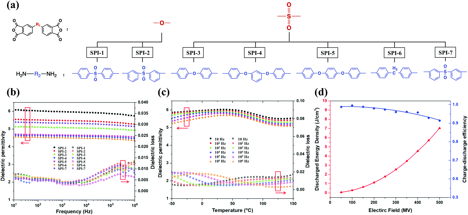 | ||
| Fig. 9 (a) Monomers of sulfonyl-containing polyimides. The εr and tanδ of sulfonyl-containing polyimides: (b) SPI-1 to SPI-7 at room temperature, (c) SPI-1 at elevated temperatures. (d) The Ue and η of SPI-1.51 | ||
Ma et al. used high-throughput DFT computations to identify polymers with high εr and band gap.15 As shown in Fig. 10(a), a series of PIs were selected as potential polymer materials. The PI of B2 (fabricated with B and 2) with the longest cross-conjugated system and polyether segment exhibited the highest εr (7.80) of all samples, but the lowest band gap (3.48 eV). A further PI with a trifluoromethyl group, which resulted in less efficient molecular packing, gave a much lower εr (2.50), but exhibited the highest band gap (3.98). As a result, a negative correlation between the band gap and εr was observed for these samples shown in Fig. 10(b and c).
 | ||
| Fig. 10 (a) Monomers of Polyimides A1–D2. (b) DFT-based initial screening results. (c) εrvs. frequency for various types of PIs at room temperature.15 | ||
δ values (<0.02; 103–107 Hz) and good thermal stability. The crosslinked polymer also showed a relatively low leakage current density due to the inhibition of ion migration and a pinhole-free surface morphology. Liaw et al. used a novel diamine to prepare poly(pyridine imide).73 The polymer also exhibited good thermal stability and high εr (4.20 at 103 Hz), which was attributed to the rigid pyridine heterocyclic diamine and the naphthyl group. Venkat et al. synthesized a fluorinated polyimide post-functionalized with pendant adamantyl esters.74 The PI had a high thermal stability (Tg = 305 °C) and εr was relatively stable (2.85–2.91) from room temperature to 250 °C at 104 Hz.
δ (<0.01) and high εr (4.5) and energy density (12 J cm−3, η > 90%).75 There are also cases of using physical methods (blending of two polymers) to reduce the restriction on the dipole to increase the εr, which will be explained in Section 3.3.
Ma et al. also used pyromellitic dianhydride and various short-chain diamines to produce PIs with high imide density.76 The εr of the synthesized homopolymers and copolymers ranged from 3.96–6.57. An improved understanding of the structure–property relationship of these PIs was obtained by combining these experimental results with the theoretical dielectric calculations from DFT.
Introducing conductive oligomers into the PI matrix is another strategy. Among them, copper phthalocyanine has attracted attention as a semiconductor. Chen et al. synthesized a homogeneous organometallic copolymer of a copper phthalocyanine oligomer grafted to polyimide (CuPc-PI) via a polycondensation between a copper phthalocyanine anhydride oligomer (o-CuPcA) and an amino-capped polyamic acid, as shown in Fig. 11(a and b).14 The CuPc-PI, containing 30 wt% o-CuPcA, showed high εr (23.2; 102 Hz) and energy density (0.55 J cm−3) in Fig. 11(c and d). The tanδ, due to dipolar polarization and interfacial polarization, was increased by increasing the o-CuPcA content and reduced by increasing the frequency.
 | ||
| Fig. 11 (a) The polycondensation between o-CuPcA and amino-capped polyamic acid. (b) The chemical structure of o-CuPcA. (c) The frequency dependent εr of the CuPc–PI films. (d) The Eb and Ue of the CuPc-PI films.14 | ||
3.3. PI blends
By mixing two or more polymers with different molecular structures and dielectric properties to combine their respective advantages, the resulting blend can result in improved energy storage performances. This is a simple and feasible preparation method that can obtain satisfactory interface compatibility. Two high-Tg glassy state dipolar polymers, i.e., PEI and poly(ether-methyl-ether-urea), are blended to improve the free volume for dipoles in the composites.77 This proved that significantly reducing the constraints in dipoles produces a higher εr without compromising the tanδ.
Researchers have tried to improve PI energy storage performances by introducing high-εr polymers such as PSF,78 LNBR,79 PVDF,80 β-CD81 and Sn-polyester.82 Regrettably, it comes at the cost of a drop in breakdown strength. A substantial increase in energy density cannot be guaranteed. At present, researchers are more inclined to pay attention to the synergistic improvement of εr and Eb.
Ahmad et al. designed all-organic blend films made of poly(arylene ether urea) (PEEU) and PI. The blend film with 15 wt% PEEU exhibited a high εr of 4.73, a low tanδ of 0.3%, a high Tg of 353 °C and the highest energy density of 5.14 J cm−3 at 495.65 MV m−1.83 Moreover, the dielectric properties of the PEEU/PI films showed excellent temperature stability in the range of −50 °C to 250 °C. Next, Ahmad et al. introduced aromatic polythiourea (ArPTU) into the PI matrix and found that the 10 wt% ArPTU blend film exhibited the highest Eb of 443 MV m−1, which was 74% higher than that of pure PI, as well as a high Ue of 4 J cm−3.84
Molecular semiconductors have higher electron affinities than dielectric polymers, which can capture the injected and excited electrons through strong electrostatic attraction as shown in Fig. 12(a and b). This can generate a larger trap energy level, compared with the insulating nanostructures in previous high-temperature polymer nanocomposites. As shown in Fig. 12(c), the latter mainly introduces trap sites by modifying the polymer chain conformation and the arrangement at the two-phase interface. Yuan et al. chose three molecular semiconductors, namely ITIC, PCBM, and DPDI, with electron affinities of 3.9, 4.2, and 4.0 eV, respectively.85 The electronegative elements in these molecules were shown in the DFT calculation of the electrostatic potential distribution in Fig. 12(d–f). Quantitative molecular surface analysis revealed more positive electrostatic potential on their surface, indicating the attraction to electrons. The activation energy associated with carrier trapping was determined by the temperature-dependent electrical conductivity results in Fig. 12(g). Obviously, the all-organic composites had higher activation energies than PEI/BNNS, indicating larger trap depths. Molecular semiconductors had a significant impact on the charge injection and transport in polymers, which were more effective than insulating nanostructures in fixing free charges. The emphasis of the evaluation was on Ue achieved at a high η level (above 90%), in order to avoid overwhelming device heating by the energy loss in the applications. At 150 °C, the Ue of the composites ranged from 3.4 to 4.5 J cm−3 with η > 90%, while that of pure PEI is only 1.0 J cm−3 (Fig. 12(h)). What is more noticeable was that the maximum Ue of the composites with η > 90% is still as high as 3.0 J cm−3 at 200 °C in Fig. 12(i). The PI composite films containing a polyconjugated ladder structure (PcLS) treated at a high temperature (480 °C) were also prepared. The PcLS-PI composite film achieved a maximum Ue of 4.33 J cm−3.
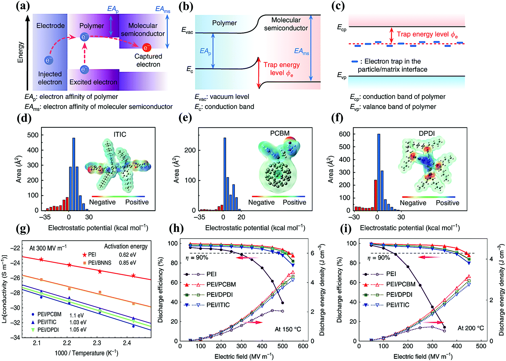 | ||
| Fig. 12 (a) Band diagram showing the possible charge transfer in the all-organic composites. Schematic illustrations of trap energy level in (b) all-organic composites and (c) polymer/insulating particle nanocomposites. Electrostatic potential distribution and area percentage in each electrostatic potential range of (d) ITIC, (e) PCBM and (f) DPDI. (g) Arrhenius function of conductivity for the pure PEI, all-organic composites and PEI/BNNS nanocomposites measured at 300 MV m−1. The energy density and discharge efficiency of PEI, PEI/PCBM, PEI/DPDI and PEI/ITIC composites at (h) 150 °C and (i) 200 °C.85 | ||
3.4. Multi-layer structures
Compared with single-layer polymer composite films formed by blending different polymers, multi-layer polymer films can easily combine the advantages of different polymer layers. In addition, the interface between adjacent layers can lead to interfacial polarization and restrain the growth of breakdown paths, leading to an increase in εr and Eb. And the design of the film as a layered structure also provides a pathway for further enhancing Ue by optimizing the stacking structures. The sandwich structure strategy is applied to improve the energy storage performance of polymer composites, and can be divided into the positive sandwich structure and the reverse sandwich structure. The basic principle of the positive sandwich structure composite is to insert a high-εr polarization layer between two insulating layers with high Eb. The insulating layer will withstand most of the applied voltage and restrain the breakdown of the nanocomposites. The reverse sandwich structure composite has high-εr polarization layers as the outer layers, and a high-Eb insulating layer as the middle layer. Wang et al. prepared positive sandwich structure films (the middle PVTC layer and the outer PEI layers), reverse sandwich structure films and single-layer blend films for comparison.87 The positive sandwich film PEI-15 vol% PVTC-PEI showed excellent temperature stability between 25 °C and 100 °C. For example, its Ue and η were mainly maintained at about 8 J cm−3 and 80%, respectively. However, the Ue of the reverse sandwich structure film 7.5 vol% PVTC-PEI-7.5 vol% PVTC had a sharp decline after 75 °C, which showed that the PEI outer layer can effectively protect the energy storage performances of the middle PVTC layer under high temperature conditions. So far, most layer-structured composite films have been designed to achieve higher Ue. However, enhanced Ue is always accompanied by suppressed η. As shown in Fig. 13(a), Sun et al. introduced a transition layer in the PEI/P(VDF-HFP) blend composite between the linear dielectric layer PEI and the nonlinear dielectric layer P (VDF-HFP), forming a unique asymmetric trilayer linear-transition-nonlinear (LTN) structure.88 Compared to single-layer films (pure PEI, pure PVDF, and blended PEI/PVDF) and PEI-P(VDF-HFP) bilayer composites, asymmetric trilayer composites with the LTN structure exhibited significantly excellent energy storage performance as shown in Fig. 13(d) and (e). The E-20 vol% E/F–F composite had obtained both a high η of 89.9% and a high Ue of 12.15 J cm−3. The composite with the LTN structure was effective for realizing the synergistic improvement of Ue and η. In Fig. 13(f), the Ue of E-20 vol% E/F–F films almost remained constant after 1.5 × 10⁵ charge–discharge cycles, indicating the outstanding cycling stability. Fig. 13(b and c) show that the radar plots intuitively illustrated the influence of the LTN structure configuration of the composite films on the energy storage performance. Compared with the symmetrical NTN structure, the asymmetrical LTN structure exhibited a lower tanδ, higher Ue and significantly improved η.
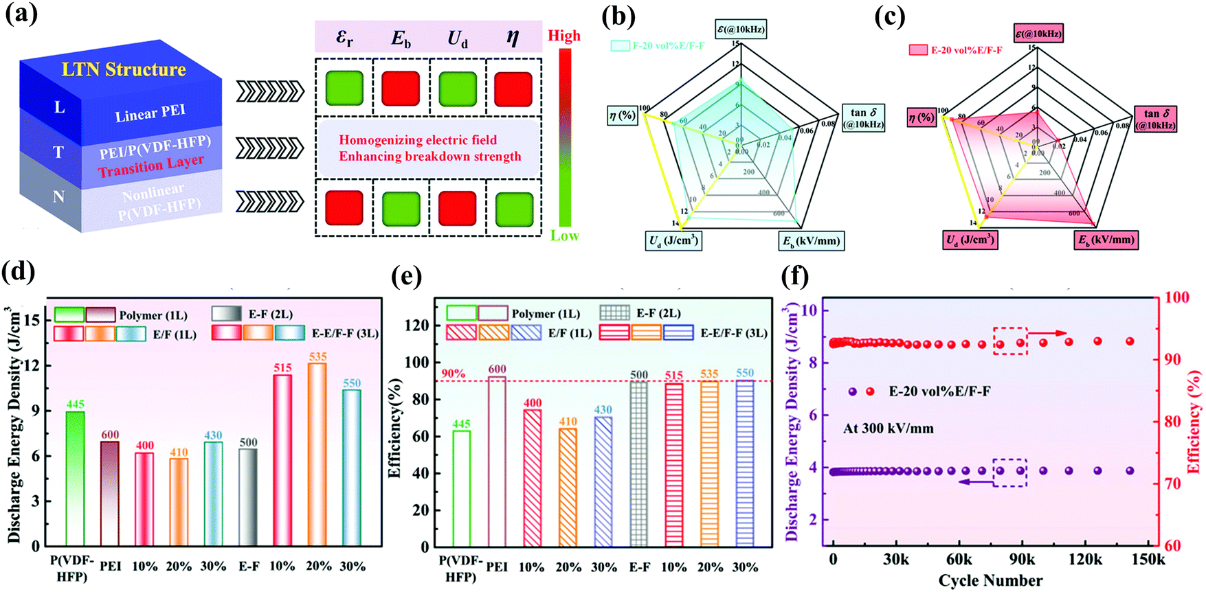 | ||
| Fig. 13 (a) Schematic illustration of the dielectric energy-storage characteristics of the asymmetric LTN structure. The radar plots of the (b) F-20 vol% E/F–F symmetric trilayer composite and (c) E-20 vol% E/F–F asymmetric trilayer composite. The (d) Ue and (e) η of pure PEI, pure P(VDF-HFP), PEI-P(VDF-HFP) bilayer composite and asymmetric trilayer composites. (f) The cycling stability performance of the E-20 vol% E/F–F asymmetric trilayer composite.88 | ||
4. PI nanocomposite dielectrics
High-temperature performance is critical for next-generation polymer dielectric capacitors operating in harsh environments. The properties of polymer matrices play an important role in determining the high temperature resistance and energy storage of composites. Composites of different polymer matrices exhibit different high-temperature dielectric properties, despite using the same fillers and preparation methods.89 Zhou et al. deposited SiO2 on both sides of a variety of polymer films (PEI-SiO2, PEN-SiO2, PI-SiO2, PC-SiO2 and FPE-SiO2) using the same production technique.90 At 150 °C, when η > 90%, the Ue value of the PEI-SiO2, PEN-SiO2, PI-SiO2, PC-SiO2 and FPE-SiO2 composite films reached 2.12, 1.75, 1.24, 1.79, and 2.06 J cm−3, which were 236, 672, 510, 1279 and 644% greater than those of the corresponding pure films, respectively. The preparation of various films demonstrated the versatility of this method. Both the PEI-SiO2 and PI-SiO2 films achieved satisfactory performance while the former attained the highest Ue value.4.1. Effects of fillers on PI nanocomposites
δ, were desirable characteristics. Li et al. prepared a ternary PEI/BTNP/BNNS nanocomposite with optimized filler compositions to provide a Ue of 2.92 J cm−3 at 150 °C.93 Ai et al. also showed that the introduction of Al2O3 or HfO2, which possessed a large band gap and a moderate εr, significantly improved Eb, Ue and η of the composites.94
The diameter and shape of nanoparticle fillers in the PI matrix caused changes in dielectric properties. Compared with BaTiO3 nanoparticle/PI (BT-NP/PI) composites, the introduction of BT nanowires showed more obvious improvement on the dielectric properties of the composites.95 Cheng et al. incorporated wide-band gap two-dimensional MoS2 into PI, and the energy density of the nanocomposite film increased to 3.35 J cm−3.96 Li et al. also explored the strong dependence of conductive behavior and Eb on the filler morphology of polymer composites.97 In addition, the effect of filler particle size was also studied. For example, the effect of alumina nanofiller particle size on the dielectric response of PEI nanocomposites was investigated.98 The composition range in which the dielectric enhancement occurs was broader for larger-size nanoparticles. Large size nanofillers required a higher volume content to achieve similar interfacial effects of smaller size nanofillers.
 | ||
| Fig. 14 Distribution of fillers in the polymer: (a) 0D fillers, (b) self-assembled 1D or 2D fillers and (c) oriented 1D or 2D fillers. Multilayer film preparation process: (d) layer-by-layer solution casting, (e) freeze-drying and (f) vapor deposition or magnetron sputtering. | ||
Multi-layer structures can be used to change the distribution of the physical field controlled by fillers, and thus improve the dielectric properties.40 The multilayer structure has been constructed using a variety of methods, such as layer-by-layer solution casting,101 freeze-drying,102 vapor deposition7 and magnetron sputtering,103 as shown in Fig. 14(d–f). For instance, when boron nitride nanosheets (BNNS) and reduced graphene oxide (RGO) were distributed in PI and assembled into a novel micro-sandwich structure, a high permittivity (∼579) and high energy density (14.2 J cm−3) were obtained.102 When a hexagonal boron nitride (h-BN) film was prepared using chemical vapor deposition (CVD) and transferred to a PEI film, the energy density of the film was 1.19 J cm−3 at 200 °C.7
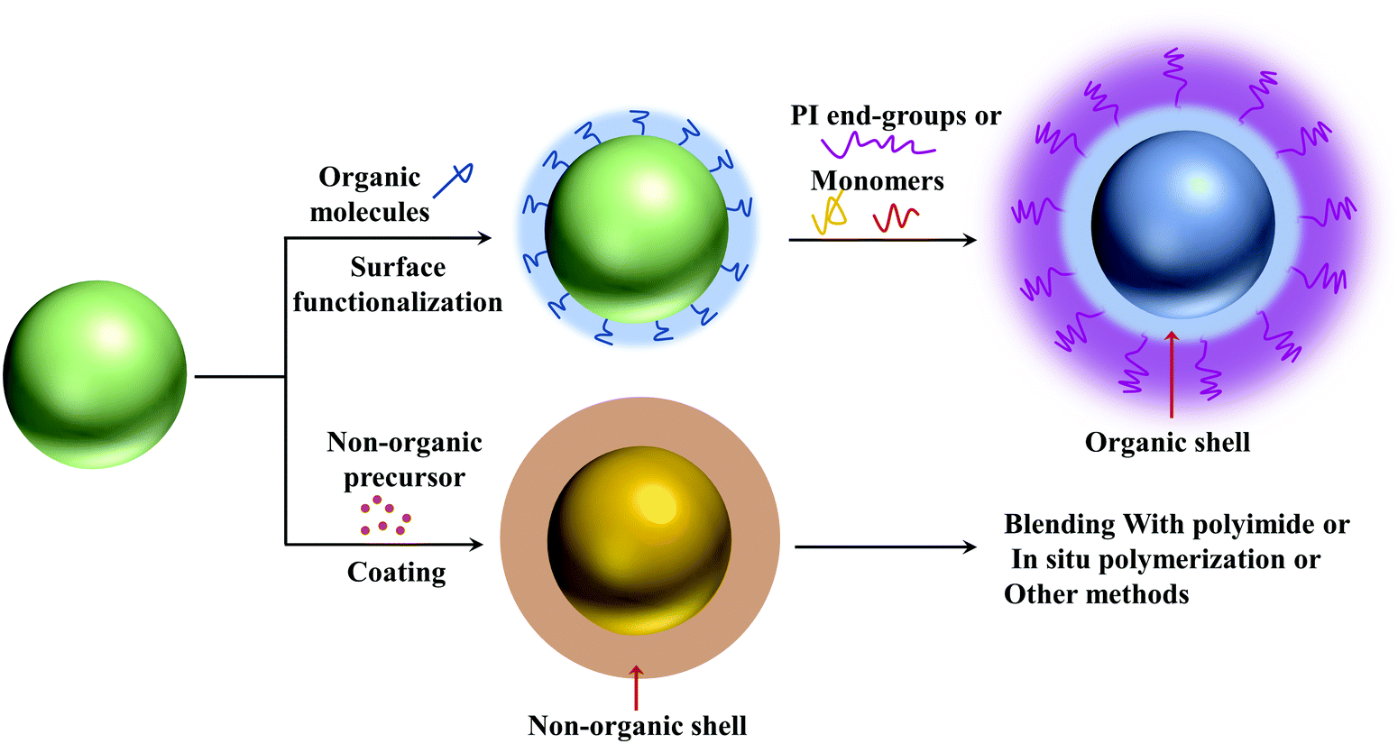 | ||
| Fig. 15 General methods for the synthesis of core–shell nanofillers for PI nanocomposites. | ||
4.1.4.1. Organic shell layers. The interaction between the nanoparticles and polymers is critical to the microstructure and even the final performances of nanocomposites. Organic shells can provide strong interaction with the nanofillers and polymer matrix, thereby improving uniform dispersion of the nanoparticles. And because of the similar chemical structure, the polymer matrix and the nanofillers with organic shells have better compatibility.
Wu et al. designed PI nanocomposites with a core–shell structure of barium titanate@polydopamine (BT@PDA) nanoparticles.104 The existence of the PDA shells optimized the dispersion uniformity and interface compatibility of BT nanoparticles in the PI matrix, thereby reducing the local electric field distortion in the nanocomposites. The PI nanocomposite containing 1 vol% BT@PDA nanoparticles exhibited the highest energy density of 1.94 J cm−3 at 315 MV m−1.
Zhu et al. modified the surface of halloysite nanotubes (HNTs) with polyaniline (PANI) to prepare PANI-HNTs/PI nanocomposite films, which exhibited an εr value of 17.3 with a low tanδ of 0.2 at 100 Hz, and a Ue of 0.93 J cm−3.105 Fang et al. coated PANI on graphene oxide (GO) using in situ polymerization to obtain GO@PANI, which then reduced with hydrazine to fabricate RGO@R-PANI.32 The obtained “insulator–conductor–insulator” structures were evenly distributed in the PI matrix. RGO nanosheets were completely isolated by R-PANI, which was conducive to the formation of a microcapacitor structure and prevented current leakage. The εr and tanδ values of the 20 wt% RGO@R-PANI/PI nanocomposite film were 25.84 and 0.11, respectively. Furthermore, the Td5% of the 20 wt% RGO@R-PANI/PI was 480 °C, indicating that the nanocomposite film has great potential in the field of high temperature dielectric materials.
Fang et al. introduced oxygen functional groups on the surface of GO to prepare NH2- and carboxyl-functionalized GO (PPD-CFGO), which participated in the in situ polymerization of PI.1 Since the polymer chains were anchored on the surface, the GO was effectively prevented from irreversible agglomeration. The εr of the 4 wt% PPD-CFGO/PI nanocomposite film was up to 36.9, which was 12.5 times higher than that of pure PI, while the tanδ was only 0.0075.
4.1.4.2. Non-organic shell layers. Organic shells may cause additional energy loss at high temperatures due to molecular relaxation and relatively poor thermal stability.10,44 It is expected that inorganic shells have better thermal stability, allowing nanofillers to obtain low energy loss. When high-εr fillers are introduced into low-εr polymers, the large difference in εr between the two phases can cause a local electric field concentration. The introduction of an inorganic buffer layer with a moderate εr is usually an effective method to achieve the desired dielectric properties of the nanocomposites. Wang et al. prepared BaTiO3@SiO2 nanofibers by electrospinning prior to the preparation of BT@SiO2/PI nanocomposite films.106 SiO2 has an extremely low tan
δ and moderate εr. The SiO2 layers that isolated the PI and BT nanofibers alleviated the electric field concentration between the two phases and enhanced the Eb of the PI nanocomposite films. Compared with the pure PI (maximum Ue = 1.42 J cm−3; Eb = 308 MV m−1), the composite film containing 3 vol% BT@SiO2 had a maximum Ue of 2.31 J cm−3 at an Eb of 346 MV m−1. The TGA results indicated that the BT@SiO2/PI nanocomposite films had good thermal stability below 500 °C. Wang et al. also adopted the same method to prepare the 2 vol% BT@ZrO2/PI composite film, which achieved a maximum Ue of 2.53 J cm−3 at an Eb of 361 MV m−1.107 The PI nanocomposites filled with CaCu3Ti4O12@TiO2 (CCTO@TiO2) nanofibers have also been studied, which obtained a maximum energy density of 1.6 J cm−3.108
Ren et al. described the PEI nanocomposites filled with core–shell structured nanoparticles composed of a ZrO2 core and an Al2O3 shell, as shown in Fig. 16(a and b).109 The introduction of the core–shell structures had achieved both improved Eb and εr, along with greatly reduced energy loss, so that high Ue was obtained. For example, Fig. 16(c) shows that the Ue of the PEI/Al2O3@ZrO2 nanocomposite is 3.11 J cm−3 and η was 92.6% at 150 °C and 400 MV m−1. In Fig. 16(d), compared to pure PEI and PEI/ZrO2 nanocomposites, the core–shell structured nanocomposites with a wide band gap Al2O3 shell show impressive improvements in dielectric and capacitance properties, including electrical resistivity, εr, Eb, Ue and η. In terms of microscopic mechanism, Fig. 16(e) shows that the hopping distance decreases from 1.32 nm of pure PEI to 1.28 and 1.12 nm of the PEI/ZrO2 and PEI/Al2O3@ZrO2 nanocomposites. The reduction in the hopping distance indicated a higher level of trap density caused by the encapsulation of the Al2O3 shell. As shown in Fig. 16(f–h), the space charge behavior in pure PEI and nanocomposites was simulated. After an electric field of 50 MV m−1 was applied, electrons and holes were gradually injected from the electrode, leading to homocharge accumulation near the electrodes. Compared with pure PEI, the space charge injection was restrained after adding ZrO2 nanoparticles, and further suppressed by using core–shell Al2O3@ZrO2 nanoparticles.
 | ||
| Fig. 16 (a) Schematic of the synthesis and (b) TEM of the Al2O3@ZrO2 nanoparticles. (c) The Ue and η, (d) leakage current density and (e) comparison of the dielectric and capacitive parameters of pure PEI, PEI/ZrO2 nanocomposites and PEI/Al2O3@ZrO2 nanocomposites at 150 °C. Simulation results of space charge distribution of (f) pure PEI, (g) PEI/ZrO2 nanocomposites and (h) PEI/Al2O3@ZrO2 nanocomposites with a decay time of 7200 s under 50 MV m−1.109 | ||
Conductive fillers often use shell structure strategies to buffer the huge difference in the dielectric permittivity of the polymer/filler two-phase interface, thereby suppressing the leakage current and reducing tanδ. Liu et al. prepared BT@GO/PI composites by the incorporation of covalently bonded BT@GO hybrids.110 The εr was as high as 285 (100 Hz), which was 80 times that of the pure PI film, and tanδ was 0.25. Similarly, Liu et al. obtained a SiO2@GO/PI composite film, which has a εr of 73 and a low tanδ of 0.38.111
In addition to coating the ceramic dielectrics on the filler surface, conductive materials such as C and Ag were also considered as new surface coatings to modify the dielectric properties of nanocomposites. Yang et al. prepared a PI embedded with CCTO/Ag nanoparticles by functionalizing the surface of CCTO nanoparticles with an Ag coating.112 At the 3% CCTO@Ag loading, the εr of the CCTO@Ag/PI nanocomposite was as high as 103 at 102 Hz. This could be attributed to the increased conductivity of the silver layer between CCTO and PI, which enhanced the space charge polarization and the Maxwell–Wagner–Sillars effect. The electric field distortion in the CCTO/PI and CCTO@Ag/PI nanocomposites was numerically simulated (COMSOL Multiphysics®). The introduction of CCTO nanoparticles resulted in high εr and high tanδ due to the pores and electric field distortion. Although Ag particles on the surface of the CCTO were conductors, the low tanδ (0.018 at 102 Hz) for CCTO@Ag/PI was due to the improved electrical distortion and blocked charge transfer by the insulating PI chains. Wang et al. prepared functionalized core–shell structure AgNW/PI hybrid films.91 The hybrid films exhibited good thermal stability (Td5% > 500 °C). The maximum εr was 126 at 102 Hz, while a relatively low dielectric loss was maintained.
4.2. Effect of multi-layer structures on PI nanocomposites
It is generally believed that the introduction of high-εr nanofillers significantly reduces the breakdown strength due to the local electric field concentration, which limits the increase in energy density to a large extent. Therefore, the simple surface modification and core–shell structure design techniques discussed in Sections 4.1.3 and 4.1.4 are explored from the perspective of fillers. Recently, dielectric polymer nanocomposites with multilayer structures have emerged to solve the paradox between high-εr and high-Eb in single-layer composite films. By systematically changing the interface, chemical structure and ratio of the constituent layers, the electric field distribution can be adjusted to greatly improve the energy density.40Table 3 summarizes the properties of multilayered PI nanocomposite films. Xie et al. used PI as the bottom insulating layer to provide high Eb, and the P(VDF-CTFE)/BT nanocomposite as the top layer to ensure high εr.113 The linear/ferroelectric bilayer dielectric material exhibited enhanced Eb and εr, which was attributed to the interface barrier and interface polarization effects between the two layers. The bilayer structure revealed the influence of the synergistic double interface effects on the energy storage performances of nanocomposites, and achieved an ultra-high Ue of 14.2 J cm−3.The structural characteristics of the sandwich structure nanocomposites bring in additional opportunities to adjust the energy storage performance. Positive sandwich structure nanocomposites have been constructed. Cai et al. used the BNNS/PI nanocomposites as the outer layers and the ZnO/PI nanocomposite as the middle layer to prepare positive sandwich structure nanocomposites (ZnO/PI-S).114 The outer layers served as an effective barrier to leakage current, thereby simultaneously improving the Eb and η, while the ZnO/PI middle layer was used to increase the εr. Due to the advantages of filler selection and structural design, the Ue of the ZnO/PI-S film can reach 5.29 J cm−3 at 150 °C. Moreover, the ZnO/PI-S film exhibited reductions in Ue and η of less than 5% over 10000 cycles at 150 °C. Chi et al. prepared composite films using 0.5Ba(Zr0.2Ti0.8)O3–0.5(Ba0.7Ca0.3)TiO3/PI (BZT-BCT/PI) with different volume fractions as the middle layer and 5 vol% h-BN/PI as the top and bottom layers.101 The h-BN in the top and bottom layers introduced good thermal and insulating properties, which improved heat dissipation and decreased the energy loss in the three-layer composite film. At 25 °C and 150 °C, the breakdown strengths and storage densities of the composite films with 1 vol% BZT-BCT were 360 and 350 MV m−1, 2.3 and 1.83 J cm−3, respectively.
The reverse sandwich structure nanocomposites also have been designed. For example, Chen et al. used pure PI (high Eb) as the middle layer with KTa0.5Nb0.5O3 nanoparticle/PI (KTN/PI) composite films as two outer layers to prepare a three-layer KTN/PI structure (t-KPI) composite film.115 The maximum Ue of t-KPI containing 2 vol% KTN was 3.0 J cm−3 at an Eb of 300 MV m−1, which was much higher than that of the single-layer KTN/PI (1.5 J cm−3, Eb 210 MV m−1).
The above sandwich-structured composite films were prepared by in situ polymerization and layer-by-layer solution casting. These solution-based methods were tedious and unsafe, and many polymers were insoluble. Azizi et al. prepared h-BN films using CVD prior to transfer onto PEI to obtain h-BN/PEI/h-BN composite films.7 At 100 °C, the Ue and η of h-BN-coated PEI could attain 2.93 J cm−3 and >90%, respectively. It was interesting to note that the h-BN/PEI/h-BN films operated efficiently and provided high energy densities at a temperature close to the Tg of the polymer, i.e. at a temperature where the dielectric properties of pure PEI usually failed. The film also showed excellent cyclability and dielectric stability at high temperatures over 55000 consecutive charge–discharge cycles. However, the preparation of the h-BN/PEI/h-BN films required multiple steps, including the transfer of BN obtained by CVD to PEI, hot pressing and removal of the catalyst layer. Zhou et al. demonstrated that improved high-temperature dielectric polymers could be prepared via a combined dielectric–barrier–discharge plasma-enhanced chemical vapor deposition (PECVD) and roll-to-roll processing.90 The method was readily adaptable to large-scale production of various surface-functionalized polymer films, as shown in Fig. 17(a). BOPP films modified each side with SiO2 (BOPP-SiO2) were prepared. The wide-band gap SiO2 layer increased the potential barrier at the electrode/dielectric interface, which impeded the charge injection and greatly reduced space charge densities. Compared with the pure BOPP films, the BOPP-SiO2 films had an improved Ue, as shown in Fig. 17(b and e). As shown in Fig. 17(c and d), various polymer dielectric films were prepared, such as PI, FPE, PEI, PEN, and PC films. At 150 °C, when η > 90%, the maximum Ue of PEI-SiO2, PEN-SiO2, PI-SiO2, PC-SiO2 and FPE-SiO2 composite films reached 2.12, 1.75, 1.24, and 1.79 J cm−3, respectively. At 100 °C and η > 90%, Ue was 3.0 J cm−3 for the PEI–SiO2 film versus 2.9 J cm−3 for the h-BN/PEI/h-BN film. Cheng et al. prepared BN/PI films using physical vapor deposition (PVD) technology, which discharged an energy density of 0.493 J cm−3 with an η of over 90% at 150 °C.103
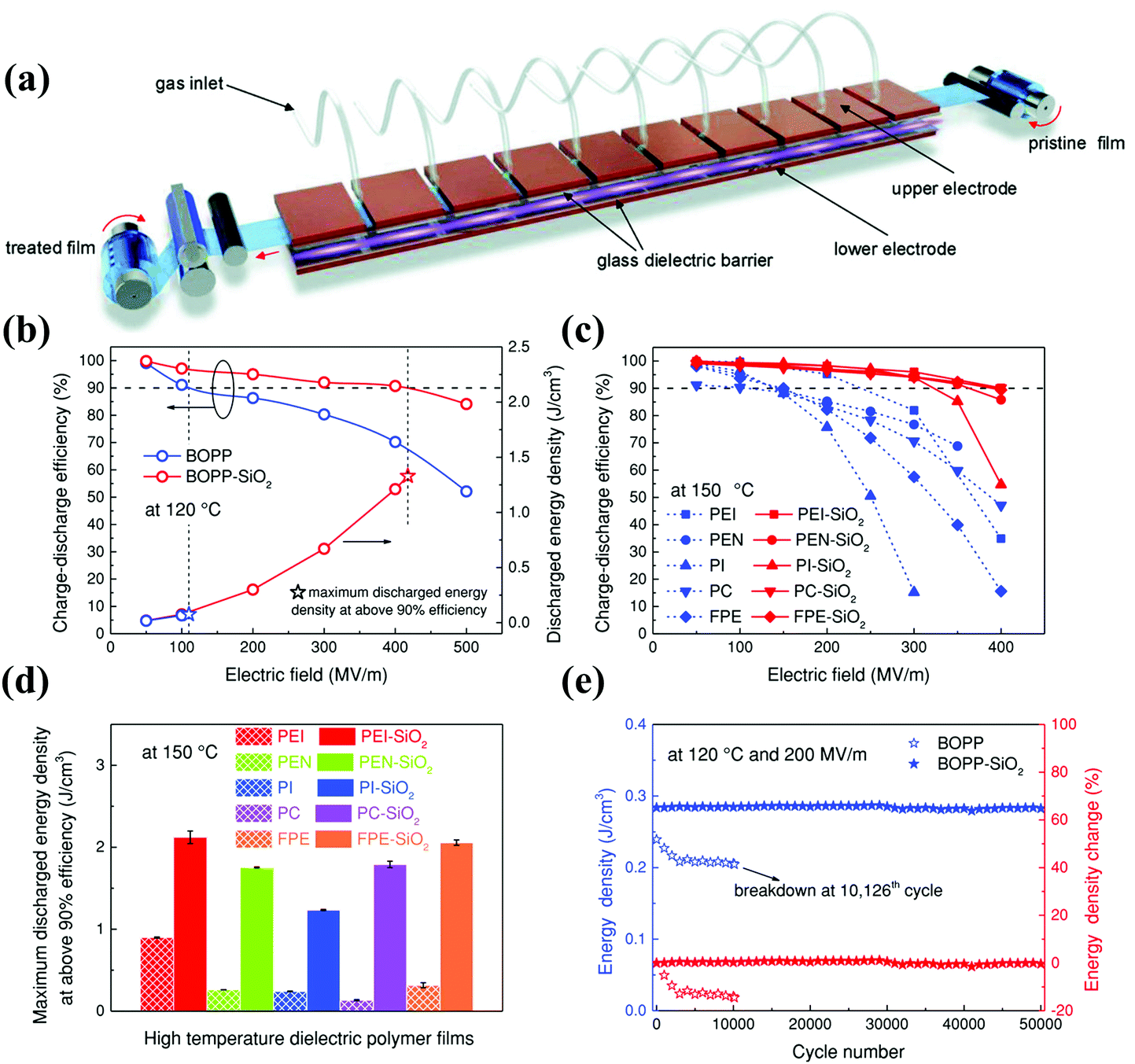 | ||
| Fig. 17 Preparation and dielectric performances of various surface-functionalized polymer films: (a) schematic of the roll-to-roll PECVD method, (b) η and Ue of BOPP and BOPP-SiO2 films at 120 °C, (c) η at 150 °C of five dielectric films, (d) maximum Ue above 90% efficiency at 150 °C of five dielectric films before and after coating, and (e) Ue obtained from cyclic fast discharge tests of BOPP and BOPP-SiO2 films.90 | ||
Guo et al. fabricated novel RGO-PI/BNNS-PI micro-sandwich composites by assembling conductive RGO and insulating BNNS layers in a PI matrix using a sequential bidirectional freeze casting technique.102 The large difference in electrical conductivities originated from the alternate stacking of RGO and BNNS has led to a high εr and a moderate Eb. The separated RGO and BNNS layers ensured that phonons were transmitted between the same species through the interface, resulting in higher thermal conductivity, as shown in Fig. 18(a). The micro-sandwich structure films achieved a high εr (∼579), low tanδ (∼0.25), high thermal conductivity (1.49 W m−1 K−1) and high energy density (14.2 J cm−3) by optimizing the filler content as shown in Fig. 18(b–e). Dong et al. fabricated a series of o-BNNS-AgNW/PI nanocomposites by combining the ice-templating self-assembly and hot-pressing technology.116 The oriented distribution of BNNS and the thermal conduction bridge formed by introducing AgNWs achieved a significant improvement in thermal conductivity. In addition, the nanocomposites maintained excellent electrical insulation properties and improved dimensional stability.
 | ||
| Fig. 18 Phonon pathways and dielectric properties of BNNS-PI, RGO-PI, and RGO-PI/BNNS-PI nanocomposites with different RGO to BNNS weight ratios: (a) phonon transport pathways in composites containing randomly mixed fillers of graphene and BNNS (A) and composites with a micro-sandwich structure (B), (b) εr, (c) tanδ, (d) AC conductivity, and (e) Eb and Ue.102 | ||
5. The devices of PI
As an excellent polymer, PI, due to its outstanding high temperature resistance, flexibility, and ease of synthesis, has made great progress in both structural and functional materials, especially in the field of energy utilization. In the energy conversion field, PI has been employed for the fabrication of devices. For example, He et al. reported a new type of dynamic piezo-thermoelectric generator, in which Bi2Te3 based devices supported by the flexible PI substrate were fixed on the outer surface of a copper tube to form an annular multi-stage energy converter.117 The generator provided a feasible solution to utilize the low-grade mechanical/thermal energy and industrial waste heat of heating fluids. A high-performance flexible thermoelectric device with PI as the substrate was also introduced, which can be used in self-powered wearable mechatronics and flexible chip cooling in the Internet of Things. Liu et al. designed and manufactured a wearable thermoelectric generator that used flexible Cu/PI electrodes.118 The device achieved a high peak power density of 13.8 mW cm−2 at a temperature difference of 50 K. Moreover, it withstood 10000 bending cycles, which indicated that the proposed wearable thermoelectric generator may provide a real-time power supply for some applied wearable electronic products in the future.
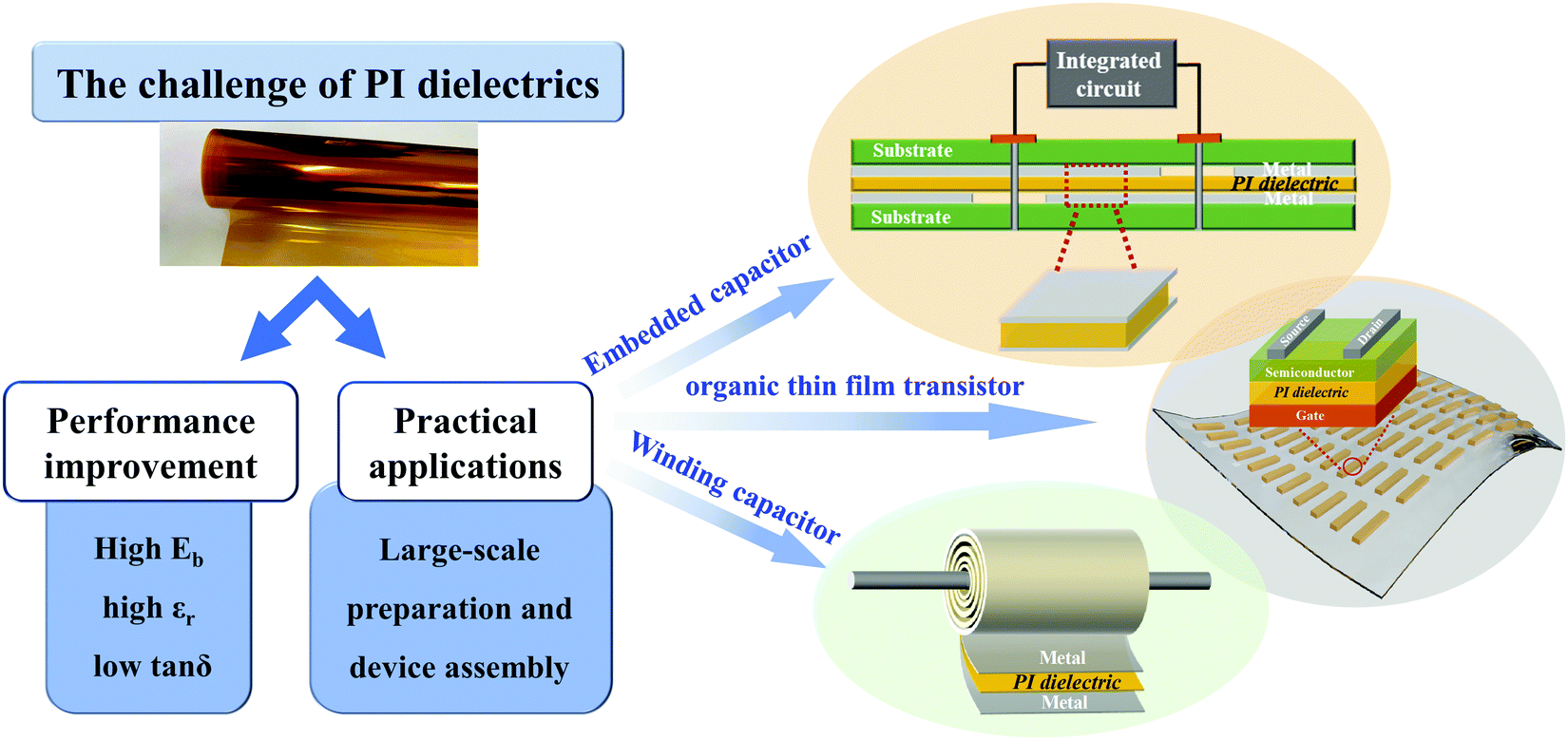
The current field of dielectric energy storage is mainly dominated by BOPP capacitor films. However, as mentioned in the previous part of the review, BOPP has a lot of drawbacks at high temperatures, forcing our research to focus on the development of PI. The academic and commercial circles have made a lot of efforts on the performance control and processing technology of PI dielectrics in this regard, as shown in Table 3. The synthesis of PI basically adopts the methods of thermal imidization, and the highest imidization temperature is mostly above 300 °C. This may be to obtain a dense structure of PI films and ensure that the PI has a sufficiently high degree of imidization. In addition to traditional solution casting methods, new PI film preparation methods such as CVD and freeze casting techniques have also begun to emerge. In terms of performance improvement, the joint adjustment mechanism of Eb, εr, and tanδ still requires continuous attention. From the perspective of application, the performances of the new all-organic PI and PI nanocomposites summarized in this review have been greatly improved, but there is no matching large-scale preparation equipment and commercial-level capacitor assembly technology. This is one of the reasons hindering the realization of commercial-grade PI capacitor assembly technology. We look forward to overcoming the challenges to apply PI dielectrics into film capacitors (such as winding capacitors, embedded capacitors etc.) and organic thin film transistors, as shown in Fig. 19. In general, there have not been enough attempts to realize PI capacitor devices. From laboratory research results to commercial products, every step here requires a lot of technical effort and interdisciplinary coordination. Fortunately, various research institutions and companies have understood the necessity of developing large-scale high-temperature-resistant dielectric films and capacitor devices.
 | ||
| Fig. 19 The challenges and the devices of PI dielectrics in the future. | ||
6. Summary and outlook
In the past few years, the research on the energy storage performances of intrinsic PI and PI composites has been intensified from the macro-scale to the micro-scale, especially at high temperatures. The focus of PI dielectric energy storage performance improvement has always been on the enhancement of εr and Eb, but it has paid a price in terms of energy loss, cost and processability. And from basic research to large-scale applications, its future still has a long way to go. Through reviewing previous work and looking forward to the future, it is believed that these strategies require researchers to pay attention.(1) From the current view, all-organic composite materials are most promising for practical applications. It can still maintain good processability while obtaining good energy storage performances. And the film forming process can be compatible with the current production process. Commercial films that can be mass-produced (such as Kapton) for organic or inorganic surface coating are also one of the feasible methods. The surface coating can have a higher uniformity of the surface structure of the polymers. Depending on the application, different types and thicknesses of coatings can be deposited on the surface of polymer films. The key factor that needs to be considered is that the selected coating material should adhere well to the polymer films and have a temperature resistance similar to or higher than that of the polymer films.
(2) Then, PI synthesis is very flexible, so the molecular structure modification of PI has great potential to be tapped. In current research, the design and synthesis of intrinsic PI dielectrics are basically focused on how to improve εr and Tg. However, more attention should be paid to the problem of tanδ in the later stage. Especially in high temperature applications, the reduction of the tanδ of the polymer dielectrics will reduce the possibility of thermal instability to improve the efficiency and reliability of the capacitor. Dipolar polarization can increase the εr while maintaining low tanδ by methods such as introducing conjugated structures or highly polar groups into the polymer main chains or side chains. To clarify the structure–property relationships of polymer dielectrics and select the appropriate polymer molecular structure and additional groups, the “co-design” method can be employed.119 This method includes high-throughput computing, materials synthesis, testing and validation. The combination of theory and experiment could greatly improve the efficiency of research. The screening conditions for polymers should not be limited to εr and band gap. These properties, together with high thermal stability, low tanδ, film formation, and mechanical properties should be considered collectively to improve the overall performances. In addition, the novel PI modified in molecular structure is basically in the laboratory preparation stage, and the reaction process and yield need to be continuously optimized. Its complicated organic synthesis method and precisely controlled film manufacturing process are far from large-scale production. Therefore, new film manufacturing methods also need to be explored.
(3) Compared with the traditional solution-mixing methods, the core–shell structure strategy provides more possibilities for optimizing the microstructure and even the electrical properties of nanocomposites. The designed polymer shell and polymer matrix have a similar chemical structure, which is critical to greatly improve the overall performance of nanocomposites. The introduced inorganic shell acts as a buffer layer to minimize the local electric field enhancement, thereby increasing the Eb of the nanocomposites. Significant progress has been made in the development of nanocomposites for high-εr and energy storage through the core–shell structure strategy. By adjusting the type and thickness of the shell layer and the two-phase interface, the nanocomposites that meet the expectations can be prepared. However, it is still very laborious to maintain a precise control of the synthesis of core–shell nanoparticles and the coordinated regulation of the overall performances of the nanocomposites. For example, how to ensure the quality of core–shell structured nanoparticles in large-scale production. And how to design the nanocomposites with low tanδ, good thermal stability and other ideal characteristics while having high εr and high Eb.
(4) Regardless of whether the multi-layer structures are all-organic composites or nanocomposites, the electric field distribution can be effectively adjusted through the combination of dielectric layers and insulating layers. While ensuring high εr, the composites can maintain a good insulating ability, thereby increasing the energy density. Candidates with high Tg that are expected to be used in the high-temperature dielectric fields have been studied to determine the effect of multilayer structures on performance, but there is still a lack of systematic exploration of their high-temperature dielectric properties, especially their temperature-dependent breakdown strength. In addition, problems concerning the optimization of structural design and the development of scalable processing methods for multi-layer structure films still need to be solved urgently.
(5) Further research should consider the effect of thermal conductivity on the performance of high-temperature capacitors. A high Tg or Tm is not sufficient to protect a polymer from failures caused by extended heating. Increasing the thermal conductivity can improve the heat dissipation and reduce the potential energy losses. Therefore, thermal conductivity is an important parameter of high-temperature capacitor films that should not be overlooked. The thermal conductivity of polymers can be improved by controlling the stacking and orientation of the chains. It can also be promoted by adding thermally conductive fillers to build conductive pathways.
(6) The application of capacitor films requires high-quality, low-cost, and fast mass production technology. The high-performance capacitor films obtained in the laboratory should be integrated into a simple energy storage device related to their potential applications, together with a large-scale production process.
(7) The depletion of non-renewable energy sources such as petroleum and coal has attracted widespread interest in the use of renewable polymer materials. Research into bio-dielectric materials such as cellulose should be expanded. In addition, a reasonable structural design inspired by nature, which improves performances by imitating the structure or characteristics of natural materials, may prove to be an effective solution.
Conflicts of interest
There are no conflicts to declare.Acknowledgements
This work was financially supported by the National Natural Science Foundation of China (No. 51977114) and Fundamental Research Funds for the Central Universities (No. FRF-NP-19-008 and FRF-TP-20-02B2, FRF-BR-20-03B).Notes and references
- X. Fang, X. Liu, Z.-K. Cui, J. Qian, J. Pan, X. Li and Q. Zhuang, J. Mater. Chem. A, 2015, 3, 10005–10012 RSC.
- M. Guo, J. Jiang, Z. Shen, Y. Lin, C.-W. Nan and Y. Shen, Mater. Today, 2019, 29, 49–67 CrossRef CAS.
- B. Fan, F. Liu, G. Yang, H. Li, G. Zhang, S. Jiang and Q. Wang, IET Nanodielectr., 2018, 1, 32–40 CrossRef.
- J. M. Wang, L. Z. Zhang, L. F. Wang, W. W. Lei and Z. S. Wu, Energy Environ. Mater., 2021, 0, 1–35 Search PubMed.
- C. Buttay, D. Planson, B. Allard, D. Bergogne, P. Bevilacqua, C. Joubert, M. Lazar, C. Martin, H. Morel, D. Tournier and C. Raynaud, Mater. Sci. Eng., B, 2011, 176, 283–288 CrossRef CAS.
- M. Rabuffi and G. Picci, IEEE Trans. Plasma Sci., 2002, 30, 1939–1942 CrossRef CAS.
- A. Azizi, M. R. Gadinski, Q. Li, M. A. AlSaud, J. Wang, Y. Wang, B. Wang, F. Liu, L. Q. Chen, N. Alem and Q. Wang, Adv. Mater., 2017, 29, 1701864 CrossRef PubMed.
- D. Tan, L. Zhang, Q. Chen and P. Irwin, J. Electron. Mater., 2014, 43, 4569–4575 CrossRef CAS.
- H. Palneedi, M. Peddigari, G.-T. Hwang, D.-Y. Jeong and J. Ryu, Adv. Funct. Mater., 2018, 28, 1803665 CrossRef.
- H. Luo, X. Zhou, C. Ellingford, Y. Zhang, S. Chen, K. Zhou, D. Zhang, C. R. Bowen and C. Wan, Chem. Soc. Rev., 2019, 48, 4424–4465 RSC.
- J. S. Ho and S. G. Greenbaum, ACS Appl. Mater. Interfaces, 2018, 10, 29189–29218 CrossRef CAS PubMed.
- Q. Li, L. Chen, M. R. Gadinski, S. Zhang, G. Zhang, H. U. Li, E. Iagodkine, A. Haque, L.-Q. Chen, T. N. Jackson and Q. Wang, Nature, 2015, 523, 576–579 CrossRef CAS PubMed.
- X. Peng, W. Xu, L. Chen, Y. Ding, T. Xiong, S. Chen and H. Hou, React. Funct. Polym., 2016, 106, 93–98 CrossRef CAS.
- L. Chen, Y. Ding, T. Yang, C. Wan and H. Hou, J. Mater. Chem. C, 2017, 5, 8371–8375 RSC.
- R. Ma, A. F. Baldwin, C. Wang, I. Offenbach, M. Cakmak, R. Ramprasad and G. A. Sotzing, ACS Appl. Mater. Interfaces, 2014, 6, 10445–10451 CrossRef CAS PubMed.
- D. H. Wang, B. A. Kurish, I. Treufeld, L. Zhu and L.-S. Tan, J. Polym. Sci., Part A: Polym. Chem., 2015, 53, 422–436 CrossRef CAS.
- A. Alias, Z. Ahmad and A. B. Ismail, Mater. Sci. Eng., B, 2011, 176, 799–804 CrossRef CAS.
- J. W. Zha, B. H. Fan, Z. M. Dang, S. T. Li and G. Chen, J. Mater. Res., 2010, 25, 2384–2391 CrossRef CAS.
- M. A. Olariu, C. Hamciuc, L. Okrasa, E. Hamciuc, L. Dimitrov and Y. Kalvachev, Polym. Compos., 2017, 38, 2584–2593 CrossRef CAS.
- J. W. Zha, H. T. Song, Z. M. Dang, C. Y. Shi and J. Bai, Appl. Phys. Lett., 2008, 93, 192911 CrossRef.
- J. W. Zha, Z. M. Dang, H. T. Song, Y. Yin and G. Chen, J. Appl. Phys., 2010, 108, 094113 CrossRef.
- J. W. Zha, Z. M. Dang, T. Zhou, H.-T. Song and G. Chen, Synth. Met., 2010, 160, 2670–2674 CrossRef CAS.
- J. W. Zha, G. Chen, Z. M. Dang and Y. Yin, J. Electrost., 2011, 69, 255–260 CrossRef CAS.
- X. Wang, Q. G. Chi, Q. Q. Lei, L. Gao and C. X. Yu, IEEE Trans. Dielectr. Electr. Insul., 2014, 21, 1471–1477 CAS.
- Q. G. Chi, J. F. Dong, C. H. Zhang, C. P. Wong, X. Wang and Q. Q. Lei, J. Mater. Chem. C, 2016, 4, 8179–8188 RSC.
- Z. M. Dang, T. Zhou, S. H. Yao, J. K. Yuan, J. W. Zha, H. T. Song, J. Y. Li, Q. Chen, W. T. Yang and J. Bai, Adv. Mater., 2009, 21, 2077–2082 CrossRef CAS.
- C. Qian, T. Zhu, W. Zheng, R. Bei, S. Liu, D. Yu, Z. Chi, Y. Zhang and J. Xu, ACS Appl. Polym. Mater., 2019, 1, 1263–1271 CrossRef CAS.
- Y. H. Wu, J. W. Zha, Z. Q. Yao, F. Sun, R. K. Y. Li and Z. M. Dang, RSC Adv., 2015, 5, 44749–44755 RSC.
- S. Yue, B. Wan, Y. Liu and Q. Zhang, RSC Adv., 2019, 9, 7706–7717 RSC.
- Z. M. Dang, Y. Q. Lin, H. P. Xu, C. Y. Shi, S. T. Li and J. B. Bai, Adv. Funct. Mater., 2008, 18, 1509–1517 CrossRef CAS.
- J. W. Zha, Q. Liu, Z. M. Dang and G. Chen, IEEE Trans. Dielectr. Electr. Insul., 2016, 23, 113–120 CAS.
- H. Feng, X. Fang, X. Liu, Q. Pei, Z. K. Cui, S. Deng, J. Gu and Q. Zhuang, Composites, Part A, 2018, 109, 578–584 CrossRef CAS.
- G. Sun, S. Zhang, Z. Yang, J. Wang, R. Chen, L. Sun, Z. Yang and S. Han, Prog. Org. Coat., 2020, 143, 105611 CrossRef CAS.
- W. Xu, Y. Ding, S. Jiang, J. Zhu, W. Ye, Y. Shen and H. Hou, Eur. Polym. J., 2014, 59, 129–135 CrossRef CAS.
- T. Akhter, S. C. Mun, S. Saeed, O. O. Park and H. M. Siddiqi, RSC Adv., 2015, 5, 71183–71189 RSC.
- J. W. Zha, F. Sun, S. J. Wang, D. Wang, X. Lin, G. Chen and Z. M. Dang, J. Appl. Phys., 2014, 116, 134104 CrossRef.
- L. Yang, X. Kong, F. Li, H. Hao, Z. Cheng, H. Liu, J. F. Li and S. Zhang, Prog. Mater. Sci., 2019, 102, 72–108 CrossRef CAS.
- Y. Qiao, X. Yin, T. Zhu, H. Li and C. Tang, Prog. Polym. Sci., 2018, 80, 153–162 CrossRef CAS.
- J. Wei and L. Zhu, Prog. Polym. Sci., 2020, 106, 101254 CrossRef CAS.
- Y. Wang, J. Chen, Y. Li, Y. Niu, Q. Wang and H. Wang, J. Mater. Chem. A, 2019, 7, 2965–2980 RSC.
- B. Fan, M. Zhou, C. Zhang, D. He and J. Bai, Prog. Polym. Sci., 2019, 97, 101143 CrossRef CAS.
- J. W. Zha, M. S. Zheng, B. H. Fan and Z. M. Dang, Nano Energy, 2021, 89, 106438 CrossRef CAS.
- Prateek, V. K. Thakur and R. K. Gupta, Chem. Rev., 2016, 116, 4260–4317 CrossRef CAS PubMed.
- X. Zhang, B. W. Li, L. Dong, H. Liu, W. Chen, Y. Shen and C. W. Nan, Adv. Mater. Interfaces, 2018, 5, 1800096 CrossRef.
- D. Q. Tan, Adv. Funct. Mater., 2019, 1808567 Search PubMed.
- X. Huang and P. Jiang, Adv. Mater., 2015, 27, 546–554 CrossRef CAS PubMed.
- Q. Li, F. Z. Yao, Y. Liu, G. Zhang, H. Wang and Q. Wang, Annu. Rev. Mater. Res., 2018, 48, 219–243 CrossRef CAS.
- N. Zhu, G. Liang, L. Yuan, Q. Guan and A. Gu, IET Nanodielectr., 2018, 1, 67–79 CrossRef.
- X. M. Zhang, J. G. Liu and S. Y. Yang, Rev. Adv. Mater. Sci., 2016, 46, 22–38 CAS.
- H. Tong, A. Ahmad, J. Fu, H. Y. Xu, T. Fan, Y. D. Hou and J. Xu, J. Appl. Polym. Sci., 2019, 136, 47883 CrossRef.
- H. Tong, J. Fu, A. Ahmad, T. Fan, Y. Hou and J. Xu, Macromol. Mater. Eng., 2019, 304, 1800709 CrossRef.
- F. C. Chiu, Adv. Mater. Sci. Eng., 2014, 1–18 CAS.
- Y. Zhou and Q. Wang, J. Appl. Phys., 2020, 127, 240902 CrossRef.
- Z. H. Shen, J. J. Wang, Y. Lin, C. W. Nan, L. Q. Chen and Y. Shen, Adv. Mater., 2018, 30, 1704380 CrossRef PubMed.
- Z. H. Shen, J. J. Wang, J. Y. Jiang, Y. H. Lin, C. W. Nan, L. Q. Chen and Y. Shen, Adv. Energy Mater., 2018, 8, 1800509 CrossRef.
- J. W. Zha, J. Lv, T. Zhou, J. K. Yuan and Z. M. Dang, J. Adv. Phys., 2012, 1, 48–53 CrossRef.
- J. W. Zha, F. Sun and Z. M. Dang, IEEE Int. C. Sol. Diel., 2013, 923–926 Search PubMed.
- S. Liu, S. Xue, S. Xiu, B. Shen and J. Zhai, Sci. Rep., 2016, 6, 26198 CrossRef CAS PubMed.
- G. Wang, X. Huang and P. Jiang, Sci. Rep., 2017, 7, 43071 CrossRef CAS PubMed.
- X. Zhang, C. Tan, Y. Ma, F. Wang and W. Yang, Compos. Sci. Technol., 2018, 162, 180–187 CrossRef CAS.
- Q. Zhao, L. Yang, K. Chen, Y. Ma, H. Ji, M. Shen, H. Huang, H. He and J. Qiu, Nano Energy, 2019, 65, 104007 CrossRef.
- Z. H. Dai, T. Li, Y. Gao, J. Xu, J. He, Y. Weng and B.-H. Guo, Compos. Sci. Technol., 2019, 169, 142–150 CrossRef CAS.
- Prateek, R. Bhunia, S. Siddiqui, A. Garg and R. K. Gupta, ACS Appl. Mater. Interfaces, 2019, 11, 14329–14339 CrossRef CAS PubMed.
- G. Chen, X. Lin, J. Li, S. Huang and X. Cheng, Appl. Surf. Sci., 2020, 513, 145877 CrossRef CAS.
- J. W. Zha, S. C. Yao, Y. Qiu, M. S. Zheng and Z. M. Dang, IET Nanodielectr., 2019, 2, 103–108 CrossRef.
- D. H. Wang, J. K. Riley, S. P. Fillery, M. F. Durstock, R. A. Vaia and L. S. Tan, J. Polym. Sci., Part A: Polym. Chem., 2013, 51, 4998–5011 CrossRef CAS.
- D. H. Wang, B. A. Kurish, I. Treufeld, L. Yang, L. Zhu and L. S. Tan, MRS Proc., 2013, 1541 Search PubMed.
- I. Treufeld, D. H. Wang, B. A. Kurish, L. S. Tan and L. Zhu, J. Mater. Chem. A, 2014, 2, 20683–20696 RSC.
- T. Zhu, Q. Yu, W. Zheng, R. Bei, W. Wang, M. Wu, S. Liu, Z. Chi, Y. Zhang and J. Xu, Polym. Chem., 2021, 12, 2481–2489 RSC.
- X. Peng, Q. Wu, S. Jiang, M. Hanif, S. Chen and H. Hou, J. Appl. Polym. Sci., 2014, 131, 40828 Search PubMed.
- T. Yang, W. Xu, X. Peng and H. Hou, RSC Adv., 2017, 7, 23309–23312 RSC.
- J. Zou, H. Wang, X. Zhang, X. Wang, Z. Shi, Y. Jiang, Z. Cui and D. Yan, J. Mater. Chem. C, 2019, 7, 7454–7459 RSC.
- D. J. Liaw, K. L. Wang, F. C. Chang, K. R. Lee and J. Y. Lai, J. Polym. Sci., Part A: Polym. Chem., 2007, 45, 2367–2374 CrossRef CAS.
- N. Venkat, T. D. Dang, Z. Bai, V. K. McNier, J. N. DeCerbo, B. H. Tsao and J. T. Stricker, Mater. Sci. Eng., B, 2010, 168, 16–21 CrossRef CAS.
- Z. Li, G. M. Treich, M. Tefferi, C. Wu, S. Nasreen, S. K. Scheirey, R. Ramprasad, G. A. Sotzing and Y. Cao, J. Mater. Chem. A, 2019, 7, 15026–15030 RSC.
- A. F. Baldwin, R. Ma, C. Wang, R. Ramprasad and G. A. Sotzing, J. Appl. Polym. Sci., 2013, 130, 1276–1280 CrossRef CAS.
- Q. Y. Zhang, X. Chen, T. Zhang and Q. M. Zhang, Nano Energy, 2019, 64, 103916 CrossRef CAS.
- P. Li, J. J. Yu, S. H. Jiang, H. Fang, K. M. Liu and H. Q. Hou, e-Polymers, 2020, 20, 226–232 CAS.
- X. Mao, B. Wu, F. F. Zhang, C. Y. Wang, T. Deng and X. Z. Tang, J. Mater. Sci.: Mater. Electron., 2019, 30, 16080–16086 CrossRef CAS.
- X. Mao, J. Yang, L. R. Du, W. F. Guo, C. Z. Li and X. Z. Tang, JOM, 2017, 69, 2497–2500 CrossRef CAS.
- C. Zhang, Y. Yu, Y. Ding, T. Yang, G. Duan and H. Hou, J. Mater. Sci.: Mater. Electron., 2017, 29, 1182–1188 CrossRef.
- S. Nasreen, M. L. Baczkowski, G. M. Treich, M. Tefferi, C. Anastasia, R. Ramprasad, Y. Cao and G. A. Sotzing, Macromol. Rapid Commun., 2018, 40, 1800679 CrossRef PubMed.
- A. Ahmad, H. Tong, T. Fan and J. Xu, J. Polym. Sci., 2021, 59, 1414–1423 CrossRef CAS.
- A. Ahmad, H. Tong, T. Fan and J. Xu, J. Appl. Polym. Sci., 2021, 138, 50997 CrossRef CAS.
- C. Yuan, Y. Zhou, Y. Zhu, J. Liang, S. Wang, S. Peng, Y. Li, S. Cheng, M. Yang, J. Hu, B. Zhang, R. Zeng, J. He and Q. Li, Nat. Commun., 2020, 11, 3919 CrossRef CAS PubMed.
- X. J. Liao, Y. C. Ding, L. L. Chen, W. Ye, J. Zhu, H. Fang and H. Q. Hou, Chem. Commun., 2015, 51, 10127–10130 RSC.
- C. Wang, G. H. He, S. Chen, D. Zhai, H. Luo and D. Zhang, J. Mater. Chem. A, 2021, 9, 8674–8684 RSC.
- L. Sun, Z. Shi, B. He, H. Wang, S. Liu, M. Huang, J. Shi, D. Dastan and H. Wang, Adv. Funct. Mater., 2021, 31, 2100280 CrossRef CAS.
- X. Huang, B. Sun, Y. Zhu, S. Li and P. Jiang, Prog. Mater. Sci., 2019, 100, 187–225 CrossRef CAS.
- Y. Zhou, Q. Li, B. Dang, Y. Yang, T. Shao, H. Li, J. Hu, R. Zeng, J. He and Q. Wang, Adv. Mater., 2018, 30, 1805672 CrossRef PubMed.
- L. Wang, X. Piao, H. Zou, Y. Wang and H. Li, Appl. Phys. A: Mater. Sci. Process., 2014, 118, 243–248 CrossRef.
- C. W. Beier, J. M. Sanders and R. L. Brutchey, J. Phys. Chem. C, 2013, 117, 6958–6965 CrossRef CAS.
- H. Li, L. L. Ren, D. Ai, Z. B. Han, Y. Liu, B. Yao and Q. Wang, InfoMat, 2020, 2, 389–400 CrossRef CAS.
- D. Ai, H. Li, Y. Zhou, L. Ren, Z. Han, B. Yao, W. Zhou, L. Zhao, J. Xu and Q. Wang, Adv. Energy Mater., 2020, 1903881 CrossRef CAS.
- M. Wang, W. L. Li, Y. Feng, Y. F. Hou, T. D. Zhang, W. D. Fei and J. H. Yin, Ceram. Int., 2015, 41, 13582–13588 CrossRef CAS.
- D. Cheng, H. Wang, B. Liu, S. Wang, Y. Li, Y. Xia and C. Xiong, J. Appl. Polym. Sci., 2019, 136, 47991 CrossRef.
- H. Li, D. Ai, L. Ren, B. Yao, Z. Han, Z. Shen, J. Wang, L. Q. Chen and Q. Wang, Adv. Mater., 2019, 31, 1900875 CrossRef PubMed.
- Y. Thakur, T. Zhang, C. Iacob, T. Yang, J. Bernholc, L. Q. Chen, J. Runt and Q. M. Zhang, Nanoscale, 2017, 9, 10992–10997 RSC.
- M. Dong, Z. Tong, P. Qi and L. Qin, J. Mater. Sci.: Mater. Electron., 2021, 32, 524–542 CrossRef CAS.
- X. Zhang, J. Jiang, Z. Shen, Z. Dan, M. Li, Y. Lin, C. W. Nan, L. Chen and Y. Shen, Adv. Mater., 2018, 30, 1707269 CrossRef PubMed.
- Q. Chi, Z. Gao, T. Zhang, C. Zhang, Y. Zhang, Q. Chen, X. Wang and Q. Lei, ACS Sustainable Chem. Eng., 2018, 7, 748–757 CrossRef.
- F. Guo, X. Shen, J. Zhou, D. Liu, Q. Zheng, J. Yang, B. Jia, A. K. T. Lau and J. K. Kim, Adv. Funct. Mater., 2020, 1910826 CrossRef CAS.
- S. Cheng, Y. Zhou, J. Hu, J. He and Q. Li, IEEE Trans. Dielectr. Electr. Insul., 2020, 27, 498–503 CAS.
- Z. Q. Wu, H. H. Zhou, Q. Guo, Z. G. Liu, L. Gong, Q. Y. Zhang, G. J. Zhong, Z. M. Li and Y. H. Chen, J. Alloys Compd., 2020, 845, 156171 CrossRef CAS.
- T. Zhu, C. Qian, W. Zheng, R. Bei, S. Liu, Z. Chi, X. Chen, Y. Zhang and J. Xu, RSC Adv., 2018, 8, 10522–10531 RSC.
- J. Wang, Y. Long, Y. Sun, X. Zhang, H. Yang and B. Lin, Appl. Surf. Sci., 2017, 426, 437–445 CrossRef CAS.
- J. Wang, Y. Sun, P. Wang, X. Yu, H. Shi, X. Zhang, H. Yang and B. Lin, J. Alloys Compd., 2019, 789, 785–791 CrossRef CAS.
- J. Wang, Y. Long, Y. Sun, X. Zhang, H. Yang and B. Lin, J. Mater. Sci.: Mater. Electron., 2018, 29, 7842–7850 CrossRef CAS.
- L. Ren, H. Li, Z. Xie, D. Ai, Y. Zhou, Y. Liu, S. Zhang, L. Yang, X. Zhao, Z. Peng, R. Liao and Q. Wang, Adv. Energy Mater., 2021, 11, 2101297 CrossRef CAS.
- L. Liu, Y. Zhang, F. Lv, W. Tong, L. Ding, P. K. Chu and P. Li, RSC Adv., 2016, 6, 86817–86823 RSC.
- L. Liu, F. Lv, Y. Zhang, P. Li, W. Tong, L. Ding and G. Zhang, Composites, Part A, 2017, 99, 41–47 CrossRef CAS.
- Y. Yang, H. Sun, D. Yin, Z. Lu, J. Wei, R. Xiong, J. Shi, Z. Wang, Z. Liu and Q. Lei, J. Mater. Chem. A, 2015, 3, 4916–4921 RSC.
- B. Xie, Q. Zhang, L. Zhang, Y. W. Zhu, X. Guo, P. Y. Fan and H. B. Zhang, Nano Energy, 2018, 54, 437–446 CrossRef CAS.
- L. X. Cai, J. M. Wu, H. M. Qin, Z. W. Li, S. Wang, G. H. Hu and C. A. X. Xiong, J. Appl. Polym. Sci., 2021, 138, 51268 CrossRef CAS.
- G. Chen, J. Lin, X. Wang, W. Yang, D. Li, W. Ding, H. Li and Q. Lei, J. Mater. Sci.: Mater. Electron., 2017, 28, 13861–13868 CrossRef CAS.
- J. Dong, L. Cao, Y. Li, Z. Wu and C. Teng, Compos. Sci. Technol., 2020, 196, 108242 CrossRef CAS.
- Y. Zhou, S. Zhang, X. Xu, W. Liu, S. Zhang, G. Li and J. He, Nano Energy, 2020, 69, 104397 CrossRef CAS.
- Y. Liu, L. Yin, W. Zhang, J. Wang, S. Hou, Z. Wu, Z. Zhang, C. Chen, X. Li, H. Ji, Q. Zhang, Z. Liu and F. Cao, Cell Rep. Phys. Sci., 2021, 2, 100412 CrossRef CAS.
- A. Mannodi-Kanakkithodi, G. M. Treich, T. D. Huan, R. Ma, M. Tefferi, Y. Cao, G. A. Sotzing and R. Ramprasad, Adv. Mater., 2016, 28, 6277–6291 CrossRef CAS PubMed.
- P. Hu, W. Sun, M. Fan, J. Qian, J. Jiang, Z. Dan, Y. Lin, C.-W. Nan, M. Li and Y. Shen, Appl. Surf. Sci., 2018, 458, 743–750 CrossRef CAS.
- J. Y. Li, J. X. Zhang, S. Z. Zhang and K. L. Ren, Macromol. Mater. Eng., 2021, 306, 2100079 CrossRef CAS.
- Y. Chen, B. Lin, X. Zhang, J. Wang, C. Lai, Y. Sun, Y. Liu and H. Yang, J. Mater. Chem. A, 2014, 2, 14118–14126 RSC.
- Q. Chi, B. Wang, T. Zhang, C. Zhang, Y. Zhang, X. Wang and Q. Lei, J. Mater. Sci.: Mater. Electron., 2019, 30, 19956–19965 CrossRef CAS.
- J. S. Ru, D. M. Min, M. Lanagan, S. T. Li and G. Chen, Mater. Des., 2021, 197, 109270 CrossRef CAS.
- Q. Chi, Z. Gao, C. Zhang, Y. Cui, J. Dong, X. Wang and Q. Lei, J. Mater. Sci.: Mater. Electron., 2017, 28, 15142–15148 CrossRef CAS.
| This journal is © The Royal Society of Chemistry 2022 |