
Development of encapsulation strategies towards the commercialization of perovskite solar cells
Sai
Ma†
,
Guizhou
Yuan†
,
Ying
Zhang
,
Ning
Yang
,
Yujing
Li
* and
Qi
Chen
 *
*
Beijing Key Laboratory of Construction Tailorable Advanced Functional Materials and Green Applications, MIIT Key Laboratory for Low-dimensional Quantum Structure and Devices, Experimental Center of Advanced Materials, School of Materials Science & Engineering, Beijing Institute of Technology, Beijing 100081, China. E-mail: qic@bit.edu.cn; yjli@bit.edu.cn
First published on 5th November 2021
Abstract
After a decade of research and development on perovskite solar cells (PSCs), the achievements targeting device stability have fallen far behind the progress made in the photoelectric conversion efficiency, which is a major obstacle in their commercialization. Although an in-depth understanding of the origin of the intrinsic and extrinsic degradation mechanisms is being rapidly acquired for these materials, the device architecture and module, together with synthetic strategies developed to improve the stability of the functional layers within the device (to inhibit phase and crystal structure transition, ion migration, morphology degradation, and surface and bulk chemical reactions), a consensus is forming that systematic encapsulation is indispensable in the device and module architecture to effectively resist harsh outdoor ageing stressors. This review, by focusing on the fundamental and technological development in the encapsulation studies of PSCs, discusses the role of encapsulation in preventing moisture and oxygen intrusion, which relies mainly on the selection of encapsulation materials, optimization of the encapsulation architecture and a more broadened sense of encapsulation to avoid the leakage of lead and improve the intrinsic stabilities of various materials in the device. Therefore, this review firstly summarizes the current state-of-the-art encapsulation approaches in various optoelectronic devices (light-emitting diodes, organic photovoltaic cells, and silicon solar cells) for their possible implications on PSCs. Then, targeting the moisture and oxygen stability, photostability, thermal stability, damp-heat stability, and thermal cycling stability, this review highlights the impact of encapsulation on these stabilities specifically. Furthermore, the authors advocate the establishment of standard and consistent procedures for the assessment of encapsulation materials and the stability of encapsulated devices for a more quantificational investigation and comparison. Finally, the current encapsulation materials are summarized for diverse techniques, developing a systematic concept of encapsulation, namely internal encapsulation, such as grain boundary encapsulation, surface and interface encapsulation, and device-level external encapsulation. This review thus offers an outlook on future material design, which may hopefully inspire future development of encapsulation technologies for PSCs.
 Sai Ma | Sai Ma received his BS degree from the Department of Materials Science and Engineering at Taiyuan University of Technology (TYUT), and MS degree from the Department of Materials Science and Engineering at the Beijing Institute of Technology (BIT). Currently, he is a PhD candidate at the Beijing Institute of Technology. His research focuses on the degradation mechanism of hybrid perovskite materials and photovoltaic devices under harsh outdoor ageing stressors. Currently, he is working on the development of perovskite-specific systematic encapsulation technology to address the stability issues of perovskite solar cells. |
 Guizhou Yuan | Guizhou Yuan received his Bachelor's degree in 2016 from the College of Chemistry & Molecular Engineering, Qingdao University of Science and Technology. Subsequently, he received his Master's degree in 2019 from the Department of Chemistry and Chemical Engineering, BIT. Currently, he is a PhD candidate in the School of Materials Science & Engineering, BIT, which he joined in 9/2019. His research interest is the long-term stability of perovskite solar cells. |
 Ying Zhang | Ying Zhang received her Bachelor's degree from the School of Materials Science & Engineering, Beijing Institute of Technology, in 2019. She is currently a Master's student under the supervision of Professor Qi Chen at the Beijing Institute of Technology. She is devoted to exploring manufacturing processing for highly efficient and stable perovskite solar cells. |
 Ning Yang | Ning Yang received her Master's degree from the School of Chemistry and Chemical Engineering, Beijing Institute of Technology in 2019. Currently, she is a PhD candidate under the supervision of Prof. Qi Chen at the School of Materials Science & Technology, Beijing Institute of Technology. Her current research interest is developing high-efficiency and stable large-scale perovskite solar cells. |
 Yujing Li | Prof. Yujing Li obtained his BS degree from the Department of Chemical Engineering at Tsinghua University, Beijing and PhD degree from the Department of Materials Science and Engineering at University of California, Los Angeles. He is currently working as professor at the School of Materials Science and Engineering at the Beijing Institute of Technology (BIT). He is interested in pursuing fundamental understanding of the degradation mechanism of materials and energy conversion devices. His research is mainly focused on the design of highly stable nanoscale structures and hybrid materials for photovoltaic, photocatalytic, and electrocatalytic applications. |
 Qi Chen | Prof. Qi Chen obtained both his BS and MS degrees from Tsinghua University, and received his PhD degree at University of California, Los Angeles (UCLA). From 2013–2016, he worked as a Postdoc Fellow at the California Nanosystems Institute (CNSI), UCLA. Currently, he is a Professor at the Beijing Institute of Technology. His research focuses on hybrid material design, processing and applications in optoelectronics for energy harvesting and storage. To date, he has published over 100 SCI papers with a total citation count of 20 |
Broader contextHalide perovskite (PVSK) materials are vulnerable to the environment due to their intrinsic instability upon exposure to oxygen, water, heat, and light. Encapsulation is of high necessity for the development of commercialized PSC modules to effectively resist the harsh outdoor ageing stressors. This review examines the current encapsulation technologies for various optoelectronic devices to determine their implications on PSCs and highlights the unique impacts of encapsulation specifically on PSC stability. It also advocates the establishment of standards, metrics, and consistent procedures for the objective assessment of encapsulation materials and the stability of encapsulated devices. Finally, it summarizes the current encapsulation materials used in different techniques. Mostly importantly, this review extends the concept of systematic encapsulation to a broader scope of device protection. In particular, internal encapsulation within PSC devices is proposed with a focus on interfaces and contacts, suggesting guidelines for future material design, which may hopefully expedite the future development of encapsulation for PSCs and PVSK-based devices. |
1. Introduction
Organic–inorganic hybrid halide perovskites represent an attractive family of semiconductor materials for optoelectronic applications, with excellent characteristics such as high absorption coefficient,1 low exciton binding energy,2 tunable band structure,3 and long carrier diffusion length,4 among others.5 In particular, they have achieved revolutionary progress in photovoltaic (PV) devices with power conversion efficiency evolving rapidly from 3.8% in 2009 to 25.5% in 2020 in single-junction devices.6–12 In 2021, the record efficiency of multiple-junction solar cells has also shown tremendous advances of up to 29.5% for monolithic tandem perovskite/Si solar cells and 21.3% for flexible tandem PSCs.13 These marvelous achievements, mainly in efficiency, are competitive with other established photovoltaic technologies (i.e., silicon, CIGS, CdTe and GaAs),14 thus meeting the requirements of commercial applications.15 In addition, the cost of perovskite-based PV technology is estimated to be lower than that of c-silicon solar cells thanks to their straightforward solution processing protocols and low material cost, which afford them great potential for commercialization.16Considering the PV tri-angle requirements for commercialization (i.e., efficiency, cost and stability), long-term stability is currently the most critical challenge for perovskite solar cells (PSCs).15,17 The device lifetime is mainly limited by two factors: the intrinsic instability of halide perovskite materials, and their moderate resistance to various external ageing stressors. Recently, it has been accepted that the intrinsic instability issues mainly stem from the soft ionic crystal nature of perovskite materials, which usually leads to their chemically active nature, including phase and crystal structure transition, ion migration, phase separation, surface and bulk chemical reaction, thermal decomposition, morphology degradation, and hygroscopicity.18
For instance, the α-FAPbI3 crystal phase, which is essential for certified devices with high efficiency, is inevitably subjected to an α-to-δ phase transition below 185 °C. The FA0.83Cs0.17Pb(I1−xBrx)3 and MAPb(I1−xBrx)3 perovskite films undergo photoinduced halide migration and phase separation, which was observed using in situ photoluminescence spectroscopy and in situ synchrotron X-ray diffraction (XRD).19 Besides, the photogenerated holes can oxidize iodide ions into neutral iodine and a large population of excited electrons can reduce Pb2+ to Pb0.20 Moreover, PSCs frequently suffer from marked performance degradation at high temperature due to the PbI2-rich and RbBr-based aggregation-induced degradation in perovskite materials. Although many intrinsic stability issues still exist in perovskite materials, a variety of chemical strategies have been reported to improve their intrinsic stability such as doping, passivation, compositional engineering, dimensional engineering, and grain boundary modification.21–26 There is some useful literature on the fundamental explanation of the decomposition mechanism and summary of useful strategies to address the stability issues in perovskite materials, which can be referred to as good learning material.27–29
Alternatively, halide perovskite materials are found to be unstable in real operation conditions, which significantly limits the device lifetime. Mainly, the ionic crystal structure and weakly-bonded organic components of perovskite materials make them vulnerable to moisture, oxygen, and heat. Consequently, the halide perovskite absorbers degrade rapidly upon exposure to these external ageing stressors, leading to a deterioration in device performance. Thus, to prevent the degradation of the device due to environmental factors, encapsulation has been employed and proven to be a straightforward and effective method to further improve the environmental stability of PSCs. A few successful attempts have been documented thus far. For example, by encapsulation with ethylene vinyl acetate (EVA), glass, and a butyl rubber edge seal, solar cells could withstand a damp heat test (85 °C/85% RH) for 1000 h with less than 10% degradation in performance. When encapsulated in the softer EVA, the PSCs withstood the temperature cycling test (−40 to 85 °C) and retained over 90% of their initial performance after 200 temperature cycles.30 The submodules (substrate area: 100 cm2) encapsulated with polyurethane (PU) maintained 97.52% of their initial efficiency after 2136 h under outdoor conditions (−10 to 70 °C).31 Recently, our group reported that PSCs encapsulated by nonpolar paraffin achieved a 1000 h operational lifetime at continuous maximum power point output in the ambient environment.32
Although encouraging progress has been made on the encapsulation of PSCs, a fundamental understanding of the encapsulation mechanisms and operational principles specifically required for PSCs is urgently needed for the development of mature and feasible encapsulation technologies for industrial application. Early in 2014, a two-step encapsulation approach with efficiency losses of less than 12% upon encapsulation was the first report for PSCs.33 This work highlighted the thermal and mechanical damage to perovskite materials resulting from the traditional high-temperature encapsulation processes widely used for c-silicon solar cells. Later, a UV-curable adhesive (UVCA) was employed in PSCs, which avoids direct contact with the device due to the volatile gases released by UVCA, which can destroy perovskite materials. It was also found that the encapsulant should possess a suitable elastic modulus, which is critical to achieve mechanical stability under the stresses of temperature fluctuations.30 Indeed, these findings have initiated studies on the encapsulation of PSCs, which faces multidisciplinary challenges involving chemistry, materials science, and electronics engineering, wherein the well-established understanding and techniques feasible for conventional solar cells can hardly be directly adopted for PSCs. We believe that a cumulative understanding from different disciplines will provide sufficient momentum to promote the development of viable encapsulation technology for PSCs.
Accordingly, in this review, we summarize the development of encapsulation for PSCs and the main challenges for ongoing research. The objective of this review is to elaborate the rational encapsulation strategies compatible with perovskite-based devices, the impact of encapsulation on various material and device stabilities, and the basic requirements of encapsulation materials. Initially, we review the intrinsic stability issues of halide perovskite materials with competent solutions and address the significance of encapsulation to improve the device resistance under the harsh and complex outdoor environment conditions. Secondly, we summarize the well-established encapsulation technologies and encapsulation materials for other optoelectronic devices as possible implications for PSCs. It should be noted, the optimization of encapsulation technologies and the selection of device external encapsulation materials are fundamental solutions to solve the first-priority problem of moisture and oxygen intrusion. Next, we elaborate the impact of encapsulation on device stability with focus on suppressing the leakage of lead, isolating moisture and oxygen, improving photostability and/or photooxidation stability, thermal and/or thermochemical stability, and resisting decomposition under damp-heat and thermal cycling tests. Also, we advocate the establishment of standard and consistent procedures for the assessment of encapsulation materials and encapsulated device stability in a more quantitative manner. Besides, the multi-functional encapsulation materials and systematic encapsulation strategies including grain boundary encapsulation, surface and interface encapsulation, device external encapsulation specifically designed for PSCs are also discussed. In the last part of this review, we summarize the current encapsulation materials, the material properties and key parameters for encapsulation. In addition, the technological progress in the encapsulation of PSCs and an outlook for future research and development in this field are included.
2. Established encapsulation techniques for optoelectronic devices
The stability of perovskite solar cells needs to be improved from two aspects, namely, intrinsic material stability and device stability against environmental factors. Based on the recent in-depth understanding on the origin of the degradation mechanisms in PSCs, synthetic approaches, such as doping, compositional engineering, dimensional engineering, grain boundary modification, and development of new functional electron/hole transporting materials, have been employed.21–26,34 Consequently, the device stability issues related to the phase and crystal structure transition, ion migration, morphology degradation, and surface and bulk chemical reaction, have been significantly addressed and improved.27–29,35 In this regard, external encapsulation is essential to further improve the stability of PSCs under their operation conditions.30–32,36–39 The essential purpose for the encapsulation of PSCs is to prevent moisture and oxygen intrusion, wherein efforts are focused on the selection of suitable encapsulants compatible with the current sealing protocols. However, to date, the reported encapsulation technique is far from mature.30,33 The device-level external encapsulation materials (encapsulants) adopted for PSCs has not yet met the industrial requirements. Herein, for LED and Si solar cells, they have already achieved industrial success and been tested by the market. The established encapsulation technologies and encapsulation materials used in these two fields may provide essential implications in the development of encapsulated PSCs. For OPVs, as photovoltaic technology still under development but with very similar technological problems to PSCs, their encapsulation protocol may also afford important lessons worthy of attention. Therefore, we provide a detailed summary of the well-established encapsulation technologies and device external encapsulation materials for these electronic devices, which can shed light on the development of encapsulation technology for PSCs.40–482.1 LED
Light-emitting diodes (LEDs) can generate light via the electroluminescence emitted by a semiconductor material upon the controlled injection of electrons and holes. As newly commercialized light-emitting devices, LEDs have received considerable attention in solid-state lighting owing to their advantages of environment-friendly, energy saving, and highly efficient nature with sufficient stability and low cost.49,50 The core materials in LED devices are mainly inorganic semiconductors such as GaN, GaAsP, InGaN and SiC, which possess excellent stability against light and heat. However, there is the possibility of delamination of their chips and circuits due to mechanical vibration or thermal shock. Besides, the accumulation of photons during the light extraction process will lead to the generation of thermal junctions, which can increase the non-radiative recombination rate and deteriorate the device performance. Thus, the performance and reliability of the device depend heavily on the encapsulation and the intrinsic properties of the encapsulant. Due to the mildness of their operation environment, the main purpose of encapsulation is to prevent the intrusion of moisture and oxygen and the generation of thermal junctions.51,52 The process for the encapsulation of LEDs involves three steps, as follows: (1) the LED chip is fixed on a bracket; (2) the PN junction is electrically wired to the electrodes of the bracket; and (3) the encapsulation materials are applied to ensure internal structural stability. A typical encapsulation process is shown in Fig. 1a.40 A detailed schematic of the encapsulation is shown in Fig. 1c.40 The key to the encapsulation of LEDs relies on the selection of encapsulation materials that can effectively isolate the device from moisture and oxygen, dissipate heat, and hence improve their operational reliability and extend their lifetime.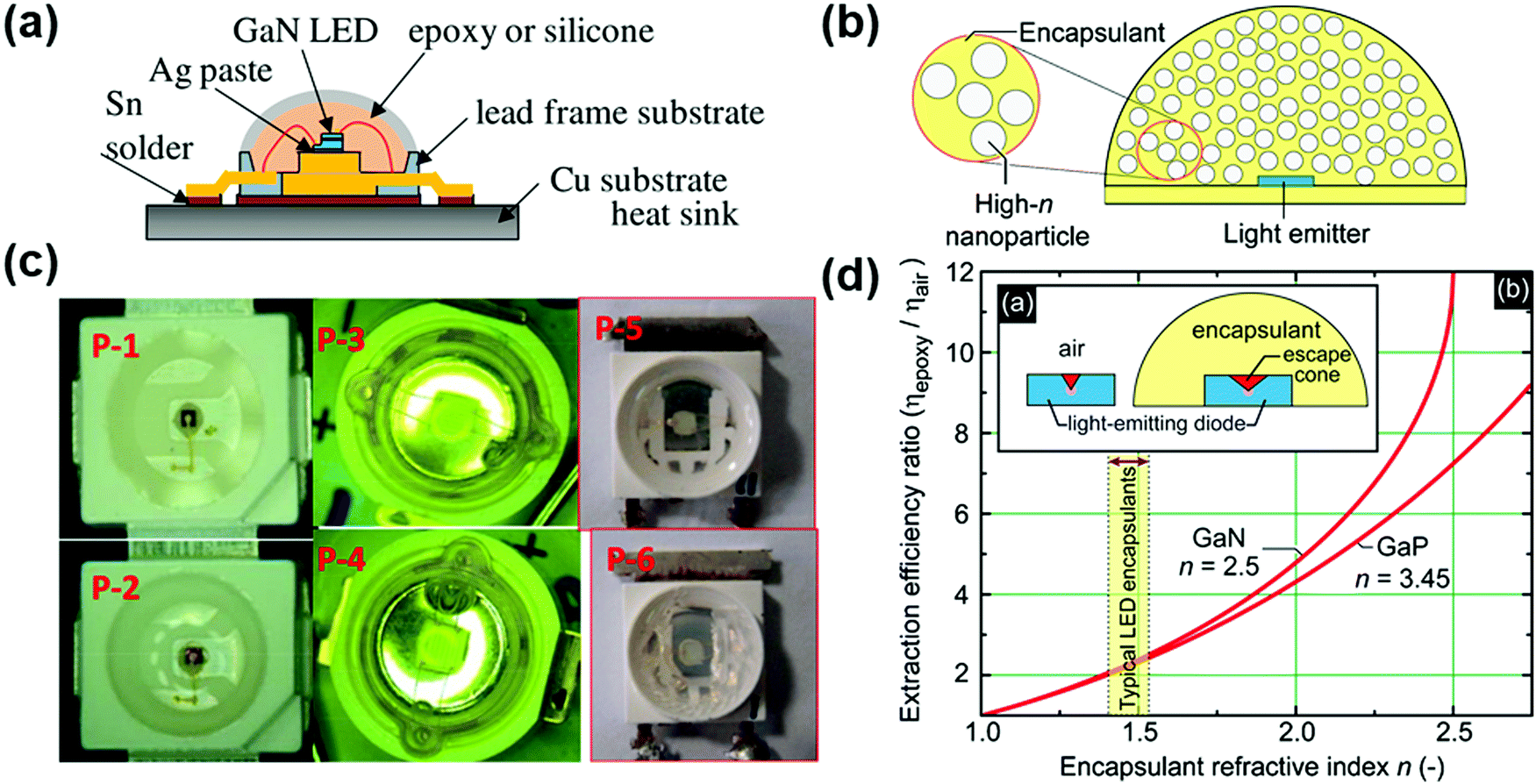 | ||
| Fig. 1 (a) Schematic of the NTF-010-K1 lead-frame for the encapsulation of P-3 and P-4. Reproduced with permission from ref. 40. Copyright 2016, Elsevier B. V. (b) Conceptual drawing of high-n nanoparticle-loaded encapsulant. Reproduced with permission from ref. 41. Copyright 2008, AIP Publishing. (c) Top-view of the LED encapsulation employed in this study. Reproduced with permission from ref. 40. Copyright 2016, Elsevier B. V. (d) (a) Escape cone of an LED without and with encapsulation and (b) light-extraction efficiency ratio for GaN and GaP as a function of the encapsulant refractive index. Reproduced with permission from ref. 41. Copyright 2008, AIP Publishing. | ||
The encapsulation materials should fulfill the following requirements: (1) an appropriate refractive index to well match the chip and improve the light extraction rate. (2) Excellent resistance to heat, oxygen, and ultraviolet irradiation. (3) A suitable coefficient of thermal expansion (CTE) that matches the LED chip to prevent delamination. (4) Extraordinary adhesion and low hygroscopicity.40,41 In this regard, two major encapsulants are commonly used for the encapsulation of LEDs. Epoxy resin is one of the widely used encapsulation materials, which is prone to ageing and discoloration, leading to a serious reduction in the light output efficiency.42 Silica gel is another commonly used encapsulation material, which has good light-thermal stability and high light transmittance.41 The transmittance of silica gel can usually reach over 97% for a wide range of light wavelengths, which can largely improve the light extraction efficiency.
Increasing the refractive index of the LED encapsulation materials can further reduce the total reflection at the interface between the film and the encapsulation material. Doping high-refractive-index scattering particles is an effective way to increase the refractive index of the encapsulation material. Mont et al. reported that the refractive index of a composite silica gel material could reach up to 1.68 through the doping of nano-TiO2 particles with a high refractive index.41 High-refractive index nanoparticles are usually dispersed uniformly in an encapsulant, as illustrated in Fig. 1b.41 By modulating the localized doping concentration, a designed refractive index gradient can be realized in the silicone material, which can further improve the light extraction efficiency (Fig. 1d).41 Besides, the UV resistance of the encapsulation materials can be enhanced by doping ZnO, and hence the lifetime of the LED can be improved.49 Thus, based on the above-mentioned analyses, it can be concluded that silicone encapsulation materials may act as good candidates for the encapsulation of optoelectronic devices.
2.2 OPV
Organic photovoltaic solar cells (OPVs) are emerging economically competitive photovoltaic technology, which feature manufacturing adaptability, low-cost processing, light weight, and flexible device architecture, attracting significant attention from scholars and the industry.43,44,53 However, organic materials are mostly reductive and highly hygroscopic, which make their components sensitive to moisture and oxygen in the ambient environment, leading to the fragility of OPV devices (Fig. 2a).45 Encapsulation technology is considered an effective solution to inhibit moisture and oxygen invasion. Fig. 2b shows the gas permeation rate through polymeric barriers described by the “solution-diffusion” model, whereby the gas molecules dissolve in the barrier, and then diffuse along a concentration gradient through the barrier.53 The total permeation rate is influenced by both the sorption and the diffusion properties of the permeant in the barrier. Meanwhile, the encapsulation materials have to meet the basic requirements of high light transmittance and mechanical strength, high electrical insulation and UV ageing resistance, reliable compatibility with devices, and low processing cost.53 Abdel-Fattah et al. investigated the air stability of bulk heterojunction (BHJ) OPV cells encapsulated with a low band gap polymer, with the cell constructed using thieno(3,4-b)-thiophene/benzodithiophene copolymer, [6,6]-phenyl C71 butyric acid methyl ester (PTB7:PC71BM) and titanium oxide (TiOx).44 This device retained its initial power conversion efficiency (PCE) in air for 20 days without significant loss. In recent years, some promising encapsulation materials, including inorganic materials such as alumina, and organic materials such as ethylene vinyl acetate (EVA)54 and polyvinyl butyral (PVB)53 are being developed for OPVs.55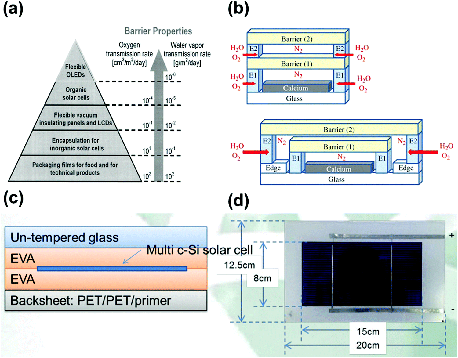 | ||
| Fig. 2 (a) Barrier requirements for different applications. Reproduced with permission from ref. 45. Copyright 2006, Electrochemical Society. (b) A calcium film encapsulated with a nitrogen gas-phase spacer between freestanding barrier films and Russian doll encapsulation architecture. Reproduced with permission from ref. 53. Copyright 2013, Elsevier Ltd. (c) Schematic of an encapsulated crystalline silicon photovoltaic solar cell. (d) A crystalline silicon photovoltaic panel. | ||
Alumina and silicon-containing materials are currently the most widely used inorganic encapsulation materials, which possess sufficient mechanical strength and high light transmittance, excellent moisture and heat resistance, and strong corrosion resistance. However, the main problems with inorganic encapsulation materials are the costly equipment required for large-scale encapsulation,56 such as plasma-enhanced chemical vapor deposition (PECVD)57 and atomic layer deposition (ALD),57 and the harsh conditions during processing, which can damage the active materials in OPVs, and thereby reduce their performances. In addition, inorganic encapsulation films are sometimes inefficient due to the existence of defects in the films, which can provide pathways for water vapor and oxygen to permeate.58
EVA, a copolymer of ethylene and vinyl acetate, is currently one of the most commonly used encapsulation materials adaptable to lamination processing. After over 30 years of research and development, the processing protocol has become mature and stable, with low cost, large-scale capability and reproducibility.59,60 EVA is cured and crosslinked after the encapsulation layers are properly fabricated and laminated at about 150 °C for 20 min. However, the main problem with EVA is its poor ageing resistance and discoloration (yellowing).61 Besides, higher lamination temperatures may also have an influence on the active materials of OPV devices. For a more detailed analysis on EVA, please refer to the following section on the encapsulation of Si solar cells.
PVB, another commonly used encapsulation material, which is different from the cross-linking EVA, is a thermoplastic material that does not cross-link during curing, whereby its chemical composition remains unchanged.55 Thus, with improved stability compared with EVA, PVB can serve as a more durable encapsulant. In addition, PVB films feature optical transparency, adhesion to glass, solar cells, and plastic, and resistance to heat, UV light and environmental influences.53 Channa et al. demonstrated solution-based barrier coatings using a composite of poly(vinyl butyral) (PVB) and mica flakes as the protection layer for a poly(3-hexylthiophene) (P3HT)-based OPV against photobleaching. The stability measurement showed that the lifetime of the OPV was extended from a few hours to over 240 h during the 1 sun test (65 °C, ambient RH%), corresponding to an extended lifetime by a factor of 9 compared to the devices encapsulated with pristine PVB.62 Bonucci et al. reported that the application of the edge-sealing EVA in addition to the standard lamination foil used in the encapsulation process could strongly reduce the moisture permeation and degradation.63
Organic silica gel, consisting of organic and inorganic materials, has achieved great development in recent years.64 Its inorganic skeleton, mainly connected by silicon-oxygen backbones (polysiloxane), possesses excellent thermal stability, chemical stability and mechanical properties, whereas its organic molecular side chain enables good flexibility, hydrophobicity, and excellent adhesion to other materials (such as glass, metal, and polyvinyl fluoride). Owing to its unique molecular structure, it also features good elasticity and toughness.65 Therefore, organic silica gel can better meet the encapsulation requirements of OPVs. By adjusting the molecular structure and components of organic silica gel, it can be adapted to the lamination and encapsulation operation at a lower temperature.66–68
2.3 Si solar cells
As the predominant photovoltaic technology, crystalline silicon solar cells have achieved commercial success after decades of development. The PCE of silicon solar cells has exceeded 27% owing to their appropriate band gap for optical absorption and excellent lattice quality for carrier transport.69,70 The lifetime of silicon solar cells can reach up to 20 years due to the excellent intrinsic stability of their covalently bonded atoms and well-developed encapsulation technology.71 Research and development on encapsulation technology of silicon photovoltaic may enlighten the development of encapsulation for PSCs.The current silicon photovoltaic industry mainly adopts three encapsulation strategies, namely, single-sided glass vacuum laminated encapsulation, double-sided glass vacuum laminated encapsulation, and non-glass encapsulation.72 Considering its practical cost and ease of processing, single-sided glass vacuum lamination encapsulation is the mainstream technique, which is processed as follows. Highly transparent tempered glass, encapsulation materials, the solar cell, encapsulation materials, and corrosion-resistant TPT (Tedlar/polyester/Tedlar) back plate are stacked in this order and laminated at high temperature and high pressure under vacuum to form solar cell modules.73,74 However, the high lamination temperature (about 150 °C) may not be suitable for the perovskite materials. A commercial silicon solar cell module can be fabricated by installing an aluminum alloy frame on the periphery of the module followed by wiring with positive and negative electrodes. In this standard encapsulation process, EVA is usually used as the encapsulation material to achieve the bonding effect between the upper tempered glass and the solar cell, as well as between the solar cell and the back plate TPT.73 A crystalline silicon solar cell and a photovoltaic panel are displayed in Fig. 2c and d, respectively.46 Recently, the encapsulation material and facility for this technology have become relatively mature, which can guarantee the lifetime of silicon solar cells for 20–25 years.
Despite the mature development of silicon photovoltaic encapsulation materials, there are still issues that require further research, such as achieving stronger adhesion with glass to reduce the path of moisture and oxygen intrusion, higher optical index matching with glass and solar cells to reduce optical loss, better electrical insulation during module operation, higher resistance to long-term corrosion and ageing, and proper mechanical strength to release stress shock.73,74 F. J. Pern et al. conducted a series of accelerated exposure test (AET) studies on crystalline-Si (c-Si) solar cells encapsulated with various superstrates, pottants, and substrates. EVA gradually turned to a yellow-brownish color upon exposure to 7.5 ultraviolet (UV) suns at 85 °C, and rapidly to dark brownish upon exposure to 9.0 UV suns at 145 °C for the glass/EVA/solar cell/EVA/glass encapsulation configuration. Exposure to 9.0 UV suns also caused severe delamination of polyester/EVA or silicone layers laminated in a polymer/EVA or silicone/solar cell/EVA or silicone/polymer configuration. For all the c-Si solar cells tested, irregular changes in their I–V parameters were observed, which could be attributed to the transmittance changes and delamination of the superstrate/pottant layers.75,76 Claudio Ferrara and Daniel Philipp investigated the performance degradation of photovoltaic modules and found that the destruction of the solar cell modules began with the yellowing or browning of the encapsulation materials due to environmental ageing.77 Thus, the stability of encapsulation materials has become the limiting factor in the lifetime of solar cells. Perovskite materials are more susceptible to degradation by external pressure sources such as moisture, oxygen, light, and heat due to the characteristics of their ionic crystals. Therefore, the encapsulation requirements of PSCs are more stringent than the current encapsulation technology of silicon photovoltaics.
In 1991, F. J. Pern and A. W. Czanderna discovered that acetic acid and polyconjugated (C![[double bond, length as m-dash]](https://www.rsc.org/images/entities/char_e001.gif) C)n double bonds of various lengths existed in an aged EVA film, together with a reduced concentration of UV light stabilizer in the film.47 Simultaneously, Bernt-Åke Sultan proposed that EVA contains a small amount of acetic acid and trace acetaldehyde in the final product due to the deacetylation reaction during thermal degradation, together with unsaturated double bonds and lactone structures.48,78 Subsequently, F. J. Pern and A. W. Czanderna discovered that the conjugated CC double bond and short-chain α,β-unsaturated carbonyl groups formed by deacetylation of the EVA film during ageing could lead to its discoloration.79 In 1996, F. J. Pern found that the ageing and discoloration of EVA are mainly affected by the cross-linking agents, curing conditions, degree of EVA cross-linking, UV radiation intensity, EVA film formulation system, and laminating curing conditions.80 In recent years, based on the understanding of these degradation mechanisms, the ageing resistance of EVA film has been successfully improved through the optimization of the cross-linking agents, antioxidants, and light stabilizers in the EVA film formulation. Meanwhile, new types of encapsulants are also being developed, such as acrylic resin adhesives, silicone rubbers, polyvinyl butyral (PVB), polyolefin elastomer (POE), and thermoplastic polyolefin (TPO).
C)n double bonds of various lengths existed in an aged EVA film, together with a reduced concentration of UV light stabilizer in the film.47 Simultaneously, Bernt-Åke Sultan proposed that EVA contains a small amount of acetic acid and trace acetaldehyde in the final product due to the deacetylation reaction during thermal degradation, together with unsaturated double bonds and lactone structures.48,78 Subsequently, F. J. Pern and A. W. Czanderna discovered that the conjugated CC double bond and short-chain α,β-unsaturated carbonyl groups formed by deacetylation of the EVA film during ageing could lead to its discoloration.79 In 1996, F. J. Pern found that the ageing and discoloration of EVA are mainly affected by the cross-linking agents, curing conditions, degree of EVA cross-linking, UV radiation intensity, EVA film formulation system, and laminating curing conditions.80 In recent years, based on the understanding of these degradation mechanisms, the ageing resistance of EVA film has been successfully improved through the optimization of the cross-linking agents, antioxidants, and light stabilizers in the EVA film formulation. Meanwhile, new types of encapsulants are also being developed, such as acrylic resin adhesives, silicone rubbers, polyvinyl butyral (PVB), polyolefin elastomer (POE), and thermoplastic polyolefin (TPO).
As previously mentioned in the OPV section, PVB is a thermoplastic material, whose intrinsic properties have already been elaborated. Here, we further discuss PVB with quantitative investigation. Yamada et al. reported an anti-reflection (AR) moth-eye structure made of acrylic resin deposited on a polyethylene terephthalate (PET) substrate. The structure was optimized in the 400–1170 nm wavelength range and achieved a reflectance of less than 1.0%. A c-Si solar cell enclosed in a PVB layer with uniform thickness was coated with the moth-eye film and found to display increased electric generation (EG) up to 15%, which was affected by the incident angle.81 Yin et al. discovered that the use of high reflective PVB foils could effectively enhance the utilization of incident light in solar cells. By optimizing the deposition of the ZnO:B films, high efficiencies of 8.8% and 10% for single-junction thin film amorphous silicon solar cells (a-Si:H, intrinsic layer thickness <200 nm) and amorphous/microcrystalline silicon tandem solar cells (a-Si:H/μc-Si:H, intrinsic amorphous silicon layer thickness <220 nm) could be achieved, respectively.55 Chen et al. incorporated PVB into dye-sensitized solar cells (DSSCs) as a quasi-solid polymeric electrolyte (SPE) thin film. The SPE devices exhibited a conversion efficiency of 5.46% at 100 mW cm−2, approximately 94% that of the corresponding liquid-electrolyte cells, with long-term durability over 3000 h.82 Huang et al. demonstrated the use of graphene (GN) as a filler to enhance the thermal conductivity of PVB composites. It showed a thermal conductivity of 4.521 W m−1 K−1 with 30 (wt%) GN, nearly 20.55 times higher than that of pure PVB, demonstrating its unique cooling function as an encapsulation material for solar cells and electronic devices.83,84
Two other materials based on a polyolefin backbone, namely POE and TPO, have also been demonstrated as encapsulants. Different from the state-of-the-art EVA encapsulant, these materials feature replacement of the vinyl acetate side groups to avoid the formation of acetic acid.85–88 Adothu et al. studied the effect of the degree of crystallinity on the thermal stability of TPO compared with the EVA. The differential scanning calorimetry (DSC) results showed that no crosslinking reaction was involved in TPO at elevated temperature, which is different from that observed for EVA. EVA showed almost the same degree of crystallinity before and after lamination, whereas TPO showed a slightly higher degree of crystallinity. The first derivative of thermogravimetry (DTG) indicated the onset of thermal degradation at 400 °C for TPO and 280 °C for EVA, implying that the TPO encapsulant possesses higher thermal stability, and hence can be an alternative to the EVA encapsulant.89 Adothu et al. also found that thermal properties of TPO remained almost unchanged, whereas EVA showed significant changes after 50 days of UV exposure. Additionally, the 180° peel adhesion test suggested that TPO displayed higher adhesion strength than EVA.90 Oreski et al. fabricated test modules with different encapsulation films including POE, TPO and EVA, and found that the devices with POE and TPO showed minor losses in their electrical performance after their manufacture. Furthermore, after the accelerated ageing test, no significant power losses were observed for the POE- and TPO-encapsulated modules. However, the test modules with EVA showed severe degradation after 3000 h of damp heat exposure, beginning with corrosion at the silver grid and above the ribbons.85
2.4 Perovskite solar cells
Although encapsulation is accepted as an indispensable procedure for the commercialization of PSCs, the development of encapsulation for PSCs is falling far behind the research progress in improving the intrinsic stability of PSCs.91 The priority of encapsulation in the field of PSCs is to solve the problem of moisture and oxygen intrusion.32 The fundamental solution relies on the selection of the encapsulation materials and optimization of encapsulation technology, which can be inspired by the in-depth investigation and well-developed encapsulation strategies in optoelectronic technologies such as LEDs, OPVs, and silicon photovoltaics. As mentioned in the previous sections, there are some mature encapsulation technologies for these devices. For LEDs, the combination of organic silica gel and heat sealing seems to be the most favored technique, owing to the excellent adhesion and low hygroscopicity, improved resistance to heat-ultraviolet ageing, and high light transmittance. For OPVs, EVA, PVB, organic silica gel, and alumina/silicon-containing compounds combined with vacuum lamination encapsulation are the most widely used technology.53 For c-Si photovoltaics, the state-of-the-art encapsulation technology with EVA, PVB, POE, TPO, organic silica gel and single-sided glass vacuum lamination effectively ensures their lifetime for over 20 years.In addition to the lessons from the well-established encapsulation technology for other optoelectronic devices, the unique encapsulation strategies specifically developed for PSCs have also made some preliminary progress. The encapsulation approaches of PSCs can be classified into three categories, as follows: (1) single-layer hydrophobic or multi-layer thin film encapsulation, (2) UV-curable adhesive encapsulation inherited from other organic electronic technologies, and (3) glass–glass vacuum laminated encapsulation adopted mainly from Si solar cells, all of which have been demonstrated to improve the stability of PSCs to some extent.56 A schematic illustration of the mainstream encapsulation methods is presented in Fig. 3.31,92–94 However, these methods also have limitations, such as insufficient anti-ageing, electrode corrosion induced by encapsulation materials, and damage to the absorber during the encapsulation process. To date, the encapsulation has effectively improved the stability of PSCs, whereby the encapsulated devices have achieved less than 10% efficiency loss under the damp heat test (85 °C/85% RH), maintained over 90% of their initial efficiency after 200 cycles of temperature cycling test (−40 to 85 °C), and retained 80% of their initial efficiency after 1000 h of maximum power point output (MPP) test.36 In the case of the decomposition mechanism, especially upon encapsulation, some fundamental research works have been reported. It has been discovered that the degradation may be induced by the deeper defect energy levels in the perovskite layer and deteriorated interface caused by phase separation and ion migration under ambient conditions.37 Moreover, the gas products of perovskite could corrode the silver electrode layer, resulting in voids in the hole-transport layer (typically spiro-OMeTAD) at high temperature and humidity (85 °C/80% RH).38,39
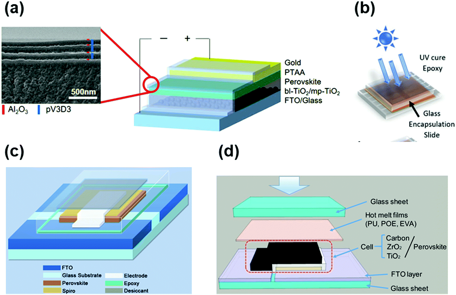 | ||
| Fig. 3 (a) (right) Schematic illustration of an encapsulated PSC and (left) cross-sectional SEM image of the TFE. Reproduced with permission from ref. 94. Copyright 2017, Wiley-VCH. (b) A schematic of the fabrication and testing routine used to create perovskite solar cells incorporating polyvinylpyrrolidone (PVP)/epoxy encapsulation. Reproduced with permission from ref. 93. Copyright 2018, Wiley-VCH. (c) Diagram of the encapsulated cell. Reproduced with permission from ref. 92. Copyright 2016, Wiley-VCH. (d) Scheme of the encapsulation of printable PSCs based on hot melt films and glass sheets. Reproduced with permission from ref. 31. Copyright 2019, Wiley-VCH. | ||
In the case of the design rationale for the encapsulation of PSCs, the priority is to solve the problem of moisture and oxygen intrusion, followed by the target to improve the intrinsic stability of the device such as preventing the leakage of lead, improving the moisture and oxygen stability, photostability and thermal stability, damp-heat stability, and thermal cycling stability. To prevent moisture and oxygen intrusion, vacuum lamination encapsulation seems to be the most suitable technique, followed by UV-curable adhesive encapsulation, and single-layer or multi-layer hydrophobic thin film encapsulation is the worst. Shi et al. reported that a device encapsulated with UV-cured epoxy retained 60% of its initial efficiency after 150 h of dark storage at 23–25 °C and an average of 50% RH condition, while the efficiency of the device encapsulated with a hot melt film remained unchanged after 200 days of storage under the same environmental condition.95 Dong et al. investigated a device encapsulated with UV-curable epoxy and found that it maintained 85% of its initial efficiency after 144 h of continuous illumination at 85 °C and 65% RH.92 Lee et al. showed that a device encapsulated with a multilayer thin-film stack of organic/inorganic layers retained 97% of its original efficiency after 300 h exposure to 50 °C and 50% RH environment.94 Some other encapsulation techniques to improve the moisture and oxygen stability could also be helpful and listed for reference.93,96–98 Therefore, given that the priority is to prevent moisture and oxygen intrusion, it relies on the selection of external encapsulation materials for the device and optimization of encapsulation technology, such as UV-curable adhesive encapsulation and vacuum lamination encapsulation. Single-layer or multi-layer hydrophobic thin film encapsulation, together with grain boundary encapsulation and interface encapsulation can be considered as internal encapsulation in the broadened sense of encapsulation to further improve the intrinsic stability of the device, which will be discussed later in detail in Section 3.
By considering these encapsulation technologies in different optoelectronic devices, some insights should be discerned, as follows: (1) single-layer or multi-layer hydrophobic thin film encapsulation can be considered an internal encapsulation strategy, which belongs to the extended meaning of systematic encapsulation. It is difficult to be classified as an independent fundamental approach due to its limited ability to prevent moisture and oxygen intrusion.56 (2) UV-curable adhesive encapsulation shows relatively improved resistance to moisture and oxygen intrusion, but it also has limitations, e.g., the resin adhesive is prone to ageing and yellowing, and a weak adhesion strength between the resin and the encapsulation substrate can lead to the invasion of moisture and oxygen.42 (3) Vacuum lamination encapsulation seems to be the most promising technology to prevent moisture and oxygen intrusion, but EVA requires a high temperature lamination process, and thus needs to be modified or replaced to be compatible with PSCs. Besides, hydrophobic fillers with weaker adhesion strength to the encapsulation substrate, e.g., organic silica gel and alumina/silicon-containing compounds, should be used to further improve the moisture and oxygen isolation.56
In short, the recent development in the encapsulation of PSCs has achieved some success by leveraging technologies from other optoelectronics, but these technologies are not entirely suitable for the encapsulation of PSCs. In addition to their unique characteristics designed for specific optoelectronic devices, problems also arise due to the insufficient understanding on PSCs under encapsulated conditions such as the destructive effect of the processing on device performance, chemical compatibility with perovskites, ageing resistance of encapsulation materials, and degradation mechanism of encapsulated PSCs. Therefore, more efforts are urgently needed to explore encapsulation technology designed specifically for perovskite photovoltaics. In the following section, we further elaborate the working principle of existing encapsulation strategies for PSCs with respect to their effect on various device stabilities, the classification of encapsulation materials, and propose an outlook for the future development of encapsulation technologies.
3. Impacts of encapsulation on PSCs
Different from other optoelectronic devices, halide perovskite solar cells suffer from instability not only due to moisture and oxygen, but also due to more diverse ageing stressors.20,99–103 Conventional encapsulation technology and device external encapsulation materials that have been widely adopted mainly focus on blocking moisture and oxygen, which unfortunately has limited capability in the protection of perovskite PV.30–32,36–39 Specifically, the encapsulated devices suffer from more severe and complex outdoor conditions such as rainfall, hail, sandstorm, insolation, and temperature fluctuations, which may lead to ion migration, overflow of volatile byproducts, film fracture, interface stratification, and module rupture.95,104–106 Additional requirements for the encapsulation of PSCs include inhibited lead leakage, improved material stability against moisture and oxygen, photostability and thermal stability, damp-heat stability, and thermal cycling stability.99,101,103 Therefore, in a broader sense, systematic encapsulation is needed for PSCs to meet the requirements for their practical applications by addressing the stability issues on multiple scales including grain boundary encapsulation, surface and interface encapsulation, and device external encapsulation.107–109 In this section, the detailed requirements are summarized to derive the fundamental targets and design rationale of a systematic encapsulation to address device stability under various conditions, and the corresponding requirements of the encapsulation materials. We also advocate the establishment of standard and consistent procedures for the stability testing of encapsulation materials and encapsulated devices for a more quantificational investigation and comparison.3.1 Lead leakage
As is known, the toxicity of lead (Pb) imposes potential health risks to human beings and severe pollution to the ecosystem in terms of genotoxicity, carcinogenicity, nephrotoxicity, neurotoxicity, immunotoxicity and reproductive toxicity.99 It has been reported that halide perovskite and its degradation products can cause significant toxicity, among which perovskite itself shows more severe toxicity than that of its individual degradation byproduct. The ecotoxicity and cytotoxicity follows the sequence of: Pb2+ > perovskite > PbI2PbO.110 From a more quantitative perspective, a study estimated the total Pb consumption (160 t per year) by assuming the deployment of halide perovskite (MAPbI3) photovoltaic in equivalence to the demand of current electricity (38 μg kW−1 h−1) in the United States as an indicator of the maximum possible Pb contamination over the lifetime of this technology. Assuming a damage rate 1% of PV modules each year, 1.6 tons of lead will be released into the environment, which may induce serious damage to the ecological system.100 Therefore, the influence of Pb species in PSCs on the environment and human health deserves more attention.
Regarding the toxicity of PSCs, we can adopt the well-established solution for the cadmium telluride (CdTe) solar cells, which also suffer the toxicity issues associated with Cd (and to a lesser extent Te). Although the heavy metal element Cd is severely toxic, CdTe is a thermally and chemically stable covalent compound with a low solubility product constant, Ksp, of 10−34, and accordingly lower toxicity (compared to pure Cd and Te).111 In contrast, the organic–inorganic hybrid perovskite materials are unstable ionic compounds with a Ksp 29 orders of magnitude higher than that of CdTe, which significantly increases their toxicity.112 Thus, to address this issue, intensive research efforts have been devoted to exploiting low-toxic/lead-free alternatives for photovoltaic applications such as tin–lead (Sn–Pb) alloyed halide perovskites, tin/germanium (Sn/Ge)-based metal halide perovskites, bismuth/antimony (Bi/Sb)-based metal halide perovskites and derivatives, copper (Cu)-based perovskites and other candidates.113 Zuo et al. reported an inverted structure based on Pb-Sn alloyed perovskites with a mitigated ecological impact (Fig. 4a).114 Wang et al. investigated an alternative mixed organic–inorganic perovskite, wherein partial Pb(II) atoms are substituted by In(III), as shown in Fig. 4b.115 However, the intrinsic stability issue of these materials, together with their low optoelectronic performance in the device, needs to be further addressed.
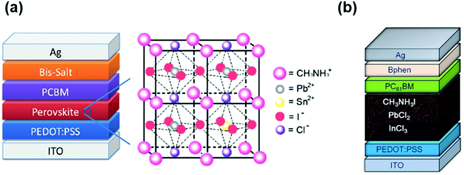 | ||
| Fig. 4 (a) Planar heterojunction solar cell based on CH3NH3Sn1−xPbxI3: device schematic structure (left) and crystal structure (right). Reproduced with permission from ref. 114. Copyright 2014, Wiley-VCH. (b) Schematic of the CH3NH3Pb0.85In0.15I3Cl0.15-based perovskite solar cell. Reproduced with permission from ref. 115. Copyright 2016, Wiley-VCH. | ||
Currently, the appropriate encapsulation of PSCs, together with cost-effective and environmentally friendly recycling programs seems to be the most straightforward and effective way to prevent Pb leakage.113 After analyzing the Pb leakage rate of an encapsulated module under different simulated weather conditions, Jiang et al. elaborated that the encapsulation methods and encapsulation materials are the critical factors in inhibiting the leakage of Pb.116 The effects of the three main encapsulation configurations were compared in this work. For the configuration adopting the conventional UVCA encapsulation method (method B), the perovskite solar modules were encapsulated by 1 mm-thick glass substrates using an ultraviolet resin at the bottom sides and coated at the edges of the modules (Fig. 5a). As a contrast to method B, 1 mm-thick glass substrates using thermo-compressed Surlyn adhesive resin films and epoxy resin (ER)-based polymer films were further added at the top sides as two other configurations, method C and method D, respectively (Fig. 5a). The rate of Pb leakage was greatly reduced for the method C and method D encapsulation configurations compared to the method B configuration, mainly due to the higher mechanical strength of the top illuminated sides. Notably, the leakage rate was reduced from 30 to 0.08 mg h−1 m−2 for the Method D configuration compared to that of method B, which was related to the self-healing ability of the ER when heated to temperatures higher than its glass transition temperature (Tg) of around 42 °C (Fig. 5b). This work highlighted that a special encapsulant, added on the top illuminated sides, with superior mechanical strength and optimal self-healing ability can largely prevent the leakage of Pb.
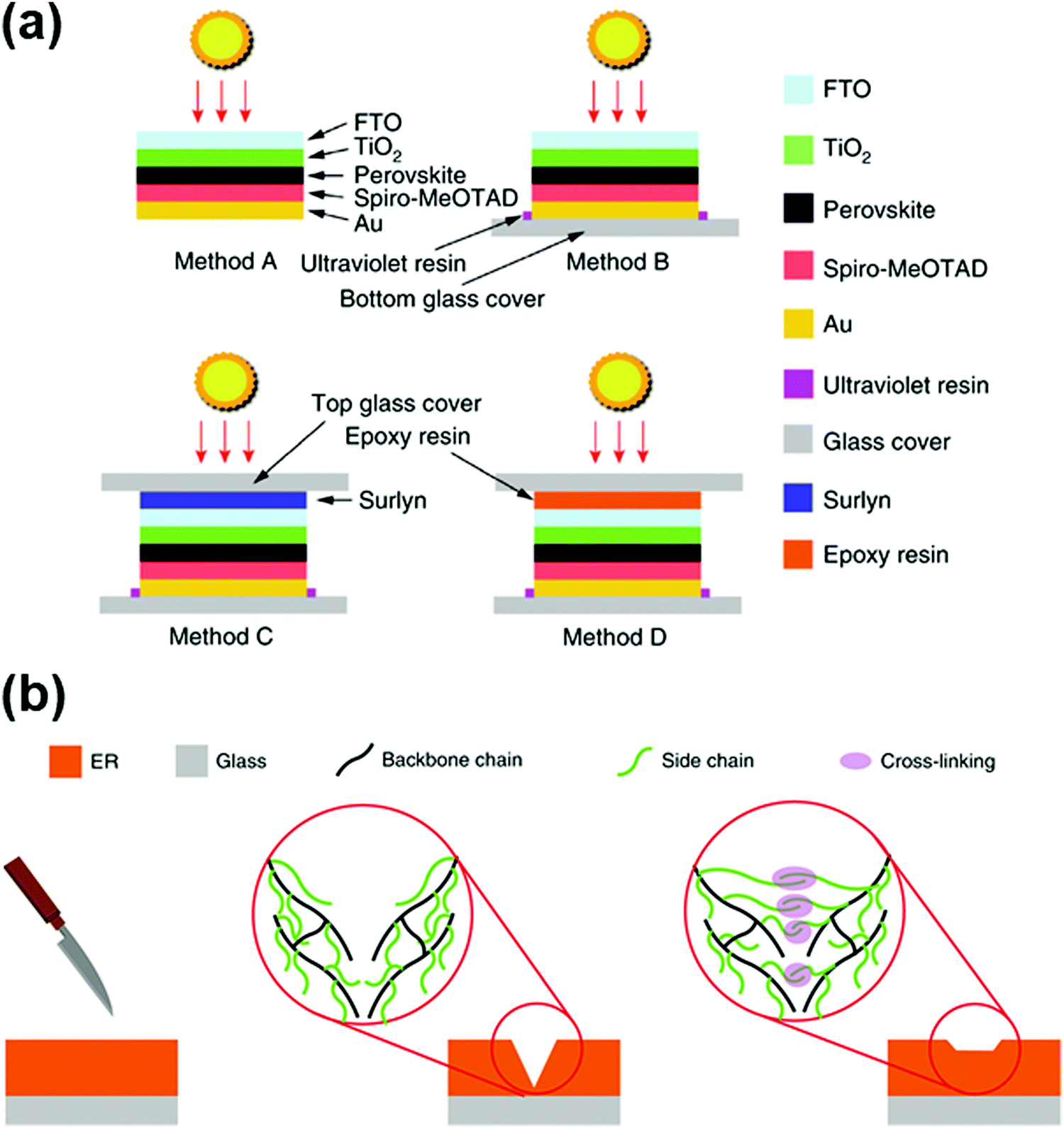 | ||
| Fig. 5 (a) Schematic showing encapsulation methods A, B, C and D. (b) Schematic showing the self-healing process of the ER encapsulant. Reproduced with permission from ref. 116. Copyright 2019, Springer Nature. | ||
3.2 Moisture and oxygen stability
Moisture and oxygen seem to be a double-edged sword for the fabrication and application of PSCs. On one hand, a proper humidity level during the annealing procedure is essential in achieving a large grain size and high-quality films, resulting in enhanced optoelectronic properties and improved mass transport processes.117 For instance, larger individual crystal and grain sizes (greater that 500 nm) with reduced pinholes and grain boundaries were obtained when the perovskite films were annealed under ambient conditions with 35% ± 5% RH.118,119 Besides, an enhanced structure reconstruction can be enabled by depositing the perovskite layer under controlled humidity conditions, resulting in substantially decreased carrier recombination. The mechanism of perovskite film formation with moisture involvement is likely to originate from the hygroscopic organic species in the CH3NH3PbX3 phases and their ionic crystal nature, where moisture may enhance the reconstruction process during film formation by partially dissolving the reactant species and accelerating mass transport within the film.117However, several groups discovered that moisture could induce reversible or irreversible degradation of perovskite films. For example, Kulbak et al. demonstrated that MAPbBr3-based devices showed a steady decay for all device parameters, leading to an average loss of 85% in efficiency, 25% in open circuit voltage, 71% in current density, and 35% in fill factor, while the CsPbBr3-based cells showed no significant decay after exposure to ambient air at a relative humidity (RH) of 60–70% for 16 days. One possible reason for this in the much higher volatility of MABr compared to CsBr. The decomposition of the perovskites with water vapor resulted in the gradual volatilization of MABr, whereas this reaction occurred at a much slower rate for CsBr. Besides, the polar organic MA cation endows MAPbBr3 a more hydrophilic nature than CsPbBr3, and thus allows water molecules to permeate faster through the edges of the devices, accelerating the decomposition rate.120,121 Noh et al. reported that MAPbI3 began to decompose at relatively high humidity (≥55%) in less than 1 day, displaying a color change from dark brown to yellow, compared with the very little degradation at low humidity (<50%) for 4 days. They intentionally exposed the solar cells to relatively high humidity (55%) for 1 day, while keeping the humidity to 35% on the following days. Interestingly, the MAPb(I1−xBrx)3 (x = 0 and 0.06) PSCs exhibited serious degradation in PCE in just less than 1 day, whereas the other MAPb(I1−xBrx)3 (x = 0.2 and 0.29) PSCs maintained their PCEs for 20 days. The low sensitivity to humidity for the cells based on MAPb(I1−xBrx)3 (x ≥ 0.2) could be associated with their compact and stable structure because the substitution of the larger I ions with the smaller Br ions in MAPb(I1−xBrx)3 leads to a reduction in the lattice constant and a transition to a cubic phase.122,123
In general, water molecules initially penetrated the perovskite structure to form an intermediate monohydrate and dihydrate phase. Meanwhile, the hydrate structures could fully revert to the dehydrated phase after 48 h in dry air (Fig. 6a).33 The incorporation of water molecules induced significant structural deformation by separating the [PbI6]4− octahedra, which caused the dehydrated structure to transform from a 3D network of octahedra to a 1D chain of octahedra for the monohydrate and a 0D framework with isolated octahedra for the dihydrate. Besides, the water molecules in perovskite crystals form strong hydrogen bonds to the organic cations, weakening the bond between the cation and the [PbI6]4− octahedra and allowing easier deprotonation of the cation and/or degradation of the film (Fig. 6b).33,124 Furthermore, the perovskite structure with water saturation could undergo irreversible degradation, creating the volatile hydroiodic acid, aqueous methylammonium iodide, and lead iodide.124 In addition to perovskite active materials, the typically used hole transport material spiro-OMETAD suffers from rapid moisture-induced degradation due to the existence of a hygroscopic lithium salt (lithium bis-(trifluoromethane)sulfonimide, Li-TFSI) as an important additive.
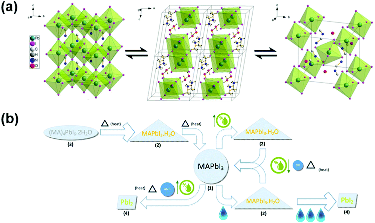 | ||
| Fig. 6 (a) (left) shows the structure of MAPI3 in its cubic phase, (middle) shows the structure of the monohydrate phase, CH3NH3PbI3·H2O, and (right) displays the structure of the dihydrate, (CH3NH3)4PbI6·2H2O. The position of the hydrogens on the CH3NH3+ ions and water are not assigned in (left) and (right). Reproduced with permission from ref. 33. Copyright 2015, American Chemical Society. (b) Degradation reaction pathway of MAPbI3 into three different pseudo-octahedral Pb–I crystalline solid complexes. Reproduced with permission from ref. 124. Copyright 2017, American Chemical Society. | ||
Oxygen also shows positive and negative impacts in terms of the efficiency and stability of PSCs. On one hand, PTAA and spiro-OMETAD, the commonly used hole transport materials for high-efficiency PSCs, require a subtle degree of oxidation to generate sufficient hole carriers in the highest occupied molecular orbital (HOMO) energy level as p-type semiconductors.125–127 Cappel et al. determined the concentrations of oxidized spiro-OMeTAD within devices under different operating and storage conditions by UV-vis spectroscopy. The relative concentrations of spiro-OMeTAD+ were found to be over 10% upon illumination in standard solid-state dye-sensitized solar cells (DSSCs), wherein no chemical dopant but oxygen and lithium ions was added during the fabrication of the solar cell. The oxidized spiro-OMeTAD was generated as a byproduct of oxygen reduction at the TiO2 surface during illumination.126 Besides, the trap states can be largely reduced and shifted downward to the valence band maximum (VBM) due to the strong affinity of oxygen molecule (O2) and oxygen atom (O) to halide vacancies, indicating that O2/O serve as p-type dopants for perovskite. This O2/O passivation can also substantially suppress the nonradiative recombination and enhance the photoluminescence (PL) of MAPbI3 by over 3 orders of magnitude, while prolonging the PL lifetime from several nanoseconds to hundreds of nanoseconds.128–131
On the other hand, the intrusion of excessive oxygen molecules would induce stability problems in the essential components, such as the hole transport materials, electron transport materials and perovskite active materials. For the hole transport materials, their conductivity, transparency, structure, and band alignment with the active layers can be regulated through the oxidation process, which influences the series resistance, shunt resistance, built-in field, free carrier extraction and defect density. Kasparavicius et al. investigated the thermal properties and long-term stability of a series of oxidized hole transport materials (HTMs). It was noticed that the oxidized HTMs started to degrade and partially reverted back to the unoxidized state and partially reacted with tBP when annealed at 100 °C.132 Wang et al. reported that the charge recombination at the TiO2/spiro-OMeTAD interface increased due to the higher amount of oxidized spiro-OMeTAD during the initial long-wavelength illumination (>450 nm).133 Thus, the oxidation process needs to be precisely controlled, and the oxidation mechanism needs to be further understood.28 For the electron transport materials (ETMs), the most typically used ETM TiO2 is a well-known photoactive catalyst used for water splitting and photocatalytic degradation of organic molecules.134,135 The adsorbed oxygen molecules at the oxygen vacancies in TiO2 can form superoxide species upon UV light exposure, which would eventually oxidize the metal halide perovskite materials.134 For perovskite active materials, Aristidou et al. suggested that molecular oxygen can reversibly adsorb and diffuse through iodide vacancies, whereby a trap state near the conduction band can be created. The charged O2− superoxide is formed upon the excitation of the perovskite, which initiates an acid–base reaction with the MA+ cation through deprotonation, forming water molecules, iodine, lead iodide, and methylamine gas.136–139
Based on the above-mentioned analyses, it can be found that moisture and oxygen influence the stability of the materials and devices through sophisticated pathways. Two strategies are usually employed to address the moisture and oxygen stability issues, as follows: (1) improving the intrinsic structural stability of the material against the destructive effects of moisture and oxygen, and (2) employing encapsulation to prevent moisture and oxygen intrusion.
Targeting the moisture stability, strategies including crystallinity engineering, element doping, grain boundary and interface modification, transport layer doping and electrode optimization have been developed. For instance, by incorporating a small amount of additive (e.g. 4-tert-butylpyridine, TBP) in the PbI2 precursor solution, a unique PbI2 nanostructure can be formed, whereby a high concentration CH3NH3I can be adopted to fabricate smooth and PbI2 residue-free high-quality perovskite films with improved efficiency and stability.26 Also, pure and highly crystalline CH3NH3PbI3 films can be formed at room temperature through the novel design of PbI2·(Py)2 precursor films.25 Besides, the partial substitution of I− with the smaller Br− or thiocyanate ion (SCN−), or replacing MA+ with the larger FA+ or with Cs+ can improve the moisture stability (35–90% RH) of PSCs by forming more stable lattice after A/B/X-site doping.123,140–144 Furthermore, modification with hydrophobic materials or insulating molecules at the grain boundaries and interfaces can effectively protect the perovskite from moisture-induced degradation, such as 2D perovskite, tetraethyl orthosilicate (TEOS), alkylalkoxysilane, oleic acid, and hydrophobic thiols (Fig. 7a).145–151 In addition, an HTM doped with hydrophobic P3HT and random copolymer (RCP) resulted in improved moisture stability by blocking the moisture in air.99,152 Jung et al. incorporated n-hexyl trimethyl ammonium bromide through post-treatment of the perovskite to create a wide-bandgap interlayer between the perovskite and HTL.8 Devices employing this layer generated substantially improved stability. The device structures are shown in Fig. 7b. For electrode optimization, carbon- and metal oxide-based electrodes, such as carbon, AZO, SnOx, ITO and MoOx, have been demonstrated and considered as promising hydrophobic electrodes to further block moisture.153,154
 | ||
| Fig. 7 (a) Schematic of surface molecular structure of perovskite film and mechanism of SAM formation between [EATZ]+ and perovskite film. Reproduced with permission from ref. 151. Copyright 2019, Wiley-VCH. (b) (left) Structure of an n–i–p perovskite solar cell based on DHA using P3HT as the hole-transport material. FTO, fluorine-doped tin oxide; d-TiO2, dense titanium dioxide; and mp-TiO2, mesoporous titanium dioxide. (Right) Schematic structure of the interface between WBH and P3HT. Reproduced with permission from ref. 8. Copyright 2019, Nature. (c) Schematic diagram of the device structure in this work: FTO/NiMgLiO/PVK/PCBM/BCP/Bi/Ag; where the Bi interlayer has superior shielding capability, prohibiting both inward and outward permeation. Reproduced with permission from ref. 161. Copyright 2019, Nature. (d) (left) Schematic representation of the structure of the perovskite solar cell, where an inverted p–i–n configuration was used, with the general FTO/PEDOT:PSS/perovskite/PCBM/PEIE/Ag structure. (right) Scheme of the solar cell adapted as a photocathode for solar H2 production. The structure remains the same, but an extra metal-encapsulating layer of FM and Pt as a HEC is added on top of the Ag layer. Reproduced with permission from ref. 102. Copyright 2016, Nature. (e) Schematic representation of the encapsulated device. Reproduced with permission from ref. 112. Copyright 2016, Royal Society of Chemistry. (f) Thin-film encapsulation with a flexible barrier. Reproduced with permission from ref. 163. Copyright 2015, Elsevier Ltd. (g) Schematic cross-section of the encapsulated perovskite solar cells. Reproduced with permission from ref. 96. Copyright 2015, Royal Society of Chemistry. | ||
In addition to improving the intrinsic structural stability, a more intuitive and direct manner to prevent water and oxygen molecule intrusion can be achieved through systematic encapsulation in a broad sense, such as grain boundary encapsulation, interface encapsulation and external encapsulation, as previously mentioned. For grain boundary encapsulation, Liu et al. demonstrated an in situ nanoscale encapsulation with silica oligomers at the grains of an FA-based perovskite to protect them from the ambient moisture, which could enhance the thermodynamic stability of the perovskite grains based on theoretical calculation.107 There are also other reports investigating the stabilizing effect of hydrophobic 2D plate-like perovskite crystallites formed at the 3D perovskite grain boundaries against moisture.149,150,155
For interface encapsulation, hydrophobic organic materials with long side-chains, polymer interlayers, and insulating oxide contact layers have been employed to keep water molecules from getting to the perovskite layer. The hydrophobic long side-chain organic materials, such as aminovaleric acid iodide (HOOC(CH2)4NH3I), alkylalkoxysilane, hydrophobic thiols, oleic acid, and polydimethylsiloxane, have been applied to the interface between the perovskite and carrier transport layer to prevent the invasion of water and oxygen, which combined with external encapsulation achieved 102–104 h moisture stability (20–80% RH) (Fig. 7e).145–147,156,157 The insulating oxide such as AZO, SnOx, ITO, and MoOx has been applied to the interface between transport layer and electrode to further resist the intrusion of water and oxygen through the electrode layer.153,154
For instance, Zhao et al. demonstrated the design of an SnOx/Ag/SnOx sandwich structure, which is regarded as an effective electrically conductive permeation barrier, to protect both the perovskite and the ultrathin silver electrode against the detrimental impact of moisture, whereby the devices maintained 81% of their initial performance after 4500 h of continuous exposure to the ambient atmosphere (23 °C and 50% RH).97,158–160 Rosungnern et al. showed that a solution-processed MoOx layer could act as a buffer layer against high moisture to suppress the generation of defects in the perovskite. The crystal structure of the perovskite with an MoOx capping layer remained unchanged after exposure to 85% RH for 30 days. The thickness of MoOx was approximately 17 nm, as determined by atomic force microscopy (AFM).153 Wang et al. found that the PSCs with a 15 nm-thick MoOx interlayer retained over 91% of their initial PCEs after exposure to 65% ± 5% RH for 30 days. In contrast, the PSCs without the MoOx interlayer sustained only 81% of their initial PCEs after 22 days. The PSCs with an MoOx interlayer showed superior stability because of the self-encapsulation effect facilitated by the hydrophobic MoOx.154 Wu et al. introduced a bismuth (Bi) interlayer between the BCP and Ag in the PSC devices with FAMACs- and MA-based perovskite.161 The Bi-interlayer-based devices exhibited greatly improved stability when exposed to humidity, thermal and light stressors, owing to the mitigated in-and-out diffusion of ions in the perovskite, while maintaining the ohmic contact between the PCBM/BCP and Ag layers (Fig. 7c).161 Zhang et al. reported a novel room-temperature post-device ligand (PDL) treatment strategy, which, on one hand, could eliminate unexpected impurities possibly introduced during the device fabrication processes, and on the other hand, improve the water stability of the device. Besides, this post-device treatment showed a special ‘stitching effect’ by self-healing the defects in the perovskite generated during the fabrication. The control devices showed fast degradation after exposure to ambient atmosphere, while the PDL-treated devices retained almost 100% of their initial PCEs after storage in 50–85% RH conditions for two weeks.162
Although abundant achievements have been reported targeting the moisture stability through grain boundary encapsulation and interface encapsulation, the commercial PSCs or modules still rely mainly on device-level external encapsulation, as “encapsulation” in a general sense, against more complex water and oxygen environments for practical application. To rely on external encapsulation to block water and oxygen intrusion, quite a few successful reported investigations can serve as references, but there are still problems to be solved. For instance, although Han et al. revealed that the encapsulated devices demonstrated improved stability, they still suffered from significant degradation after prolonged ageing at high humidity.96 The impacts of the external encapsulation on the moisture and oxygen stability can mainly be discussed from three aspects.
(1) Overall, the electrical feedthrough can be the primary pathway for water oxygen intrusion. Weerasinghe et al. pointed out that the ingress of moisture was mainly through the electrical contacts given that the completely encapsulated devices were stable for over 500 h in ambient moisture (Fig. 7f).163 Thin film encapsulation can be promising for flexible perovskite solar cells if a low-WVTR barrier can be deposited. Shi et al. also pointed out that the devices with FTO feedthroughs outperformed the devices with gold film feedthroughs. They demonstrated that a clean and metal-free surface could be highly effective for PIB to serve as an optimal moisture barrier through the Ca test.95
(2) The structure-function relation between the physical properties of the encapsulants and their performance as moisture barrier layers is worthy of in-depth investigation. Kempe et al. utilized butyl rubber as edge encapsulation with an adhesion width of 1.25 cm modeling the module architecture, together with the incorporation of a desiccant. They concluded that the encapsulation structure could be adequate for a 25-year lifetime due to its effectiveness in mitigating the moisture ingress.164 McKenna et al. compared the degradation rates of polymer-encapsulated CH3NH3PbI3−xClx films at 60 °C in air and concluded that the polymers with a low WVTR and an appropriate Tg well above the typical operating temperatures would be favored as barrier layers to improve the stability. Notably, the PMMA-encapsulated films showed no significant degradation after 384 h ageing. For other polymers, the total performance degradation could be observed at 380 h for polycarbonate (PC), 75 h for ethyl cellulose (EC), and 150 h for poly(4-methyl-1-pentene)) (PMP), following the same trend as their WVTRs (g m−2 per 24 h), i.e., 55.2 for PMMA, 115 for PC, 594![[thin space (1/6-em)]](https://www.rsc.org/images/entities/char_2009.gif) 000 for EC, and 775 for PMP, respectively.101 The requirements of WVTR for the encapsulation materials can be found in Fig. 2a and Tables 5–7.45,56 Some other quantitative research regarding the dependence of the degradation rates on the WVTR is listed for reference.94,165,166 Han et al. noted that direct contact with the perovskite device should be avoided when employing UV-cured adhesives to prevent the decomposition products from corroding the device (Fig. 7g).96 Wong-Stringer et al. found that the encapsulation system containing PVP and epoxy could serve as an efficient barrier to moisture and oxygen. They proposed that the PVP polymer could act as a barrier to mitigate the influence of epoxy on the PV device before it was fully cured.93 Recently, out group also reported that an encapsulation system with nonpolar paraffin and epoxy demonstrated negligible device efficiency degradation after 2200 h of storage in the ambient environment with 50% RH, given that the hydrophobic encapsulation materials and the nonpolar paraffin are chemically compatible with perovskite absorber.32
000 for EC, and 775 for PMP, respectively.101 The requirements of WVTR for the encapsulation materials can be found in Fig. 2a and Tables 5–7.45,56 Some other quantitative research regarding the dependence of the degradation rates on the WVTR is listed for reference.94,165,166 Han et al. noted that direct contact with the perovskite device should be avoided when employing UV-cured adhesives to prevent the decomposition products from corroding the device (Fig. 7g).96 Wong-Stringer et al. found that the encapsulation system containing PVP and epoxy could serve as an efficient barrier to moisture and oxygen. They proposed that the PVP polymer could act as a barrier to mitigate the influence of epoxy on the PV device before it was fully cured.93 Recently, out group also reported that an encapsulation system with nonpolar paraffin and epoxy demonstrated negligible device efficiency degradation after 2200 h of storage in the ambient environment with 50% RH, given that the hydrophobic encapsulation materials and the nonpolar paraffin are chemically compatible with perovskite absorber.32
(3) Lastly, encapsulation technologies with appropriate encapsulation materials and compatible encapsulation processing protocols are worthy of attention. Matteocci et al. noted that the typical processing conditions during the encapsulation, such as thermal stress, UV curing, and high pressure, could result in a loss of efficiency after encapsulation. An optimized encapsulation procedure could sustain the initial PCE value for over 1300 h of shelf-life.167 Fu et al. also investigated the influence of thermal stress in the encapsulation process on device performance, where the as-fabricated submodules could maintain 97.52% of their initial efficiency after 2136 h in outdoor conditions.31 There are also some novel encapsulation techniques developed for PSCs-based systems. For instance, the fusible InBiSn alloy was employed as an encapsulation material in a photoelectrocatalytic system developed for hydrogen evolution by fully immersing it in an aqueous solution. Self-encapsulation was proposed in semi-transparent devices with enhanced water-soaking stability (Fig. 7d).102
3.3 Stability against light immersion ageing
Light illumination is indispensable during the operation of PSCs, which can also lead to device instability. Thus, it is not feasible to use a semiconductor material for photovoltaic applications that is unstable due to prolonged light exposure. Therefore, light may also serve as a double-edged sword for the operation of PSCs. On one hand, the photo-enhanced ion conduction, i.e., the migration of iodine ions from the lattice site to the interstitial site, relies on its oxidation by the holes generated by photons.20,102 Besides, the light-induced lattice expansion in hybrid perovskite thin films can relax the local lattice strain, and hence lower the energy barrier for carrier transport at the perovskite-contact interfaces, which improves the open circuit voltage, fill factor and photostability.168 However, many studies have reported destructive changes, e.g., phase segregation and compositional degradation, occurring in perovskite films and the transport layers induced by illumination, including photooxidation reactions, photochemical reactions, and ion migration. The light-induced reactions in the perovskite film are briefly summarized as follows.(1) The influence of the photooxidation reaction (coupling of light and oxygen) on the transport layer materials and perovskite materials has been elaborated in Section 3.2. In the case of photochemical reactions, the photogenerated holes can oxidize iodide ions to form coupled neutral interstitial iodine and iodide vacancies. Meanwhile, a large population of excited electrons trapped at the iodide vacancies can reduce Pb2+ to Pb0 (Fig. 8a).169 Several studies have corroborated the existence of Pb0, together with a variety of defects, upon continuous illumination for ∼101 min to hours. The Pb0 species slowly decreased after the removal of illumination, as determined by X-ray photoemission spectroscopy (XPS).169–171 Furthermore, these works have also clarified the wavelength range of light that can cause the photochemical reaction in the perovskite active layers. Cappel et al. investigated the structural evolution of a mixed-ion perovskite ((FAPbI3)0.85(MAPbBr3)0.15) by taking advantage of the element specificity and chemical sensitivity of core-level photoelectron spectroscopy under visible laser illumination (515 nm). They observed that the laser illumination caused partially reversible chemistry in the surface region, which could be related to the phase separation into Br−- and I−-rich phases and the formation of Pb0 in the perovskite.169 Li et al. investigated the degradation of a CH3NH3PbI3 film irradiated by a blue laser (408 nm) under ultrahigh vacuum, wherein the Pb0 species started to appear in the XPS spectrum after 120 min of irradiation, indicating the decomposition of the film. The decomposition ceased after about 480 min of irradiation when the Pb0/Pb ratio reached about 33%.170 Besides, Tang et al. found that CH3NH3PbI3 could be converted to Pb0 when exposed to vacuum and white light illumination (composed of two broad peaks at 450 nm and 560 nm). They observed the formation of a series of lead salts (e.g., PbO, Pb(OH)2 and PbCO3) when CH3NH3PbI3 degraded under environmental conditions, i.e., under the combination of light, oxygen and moisture.171
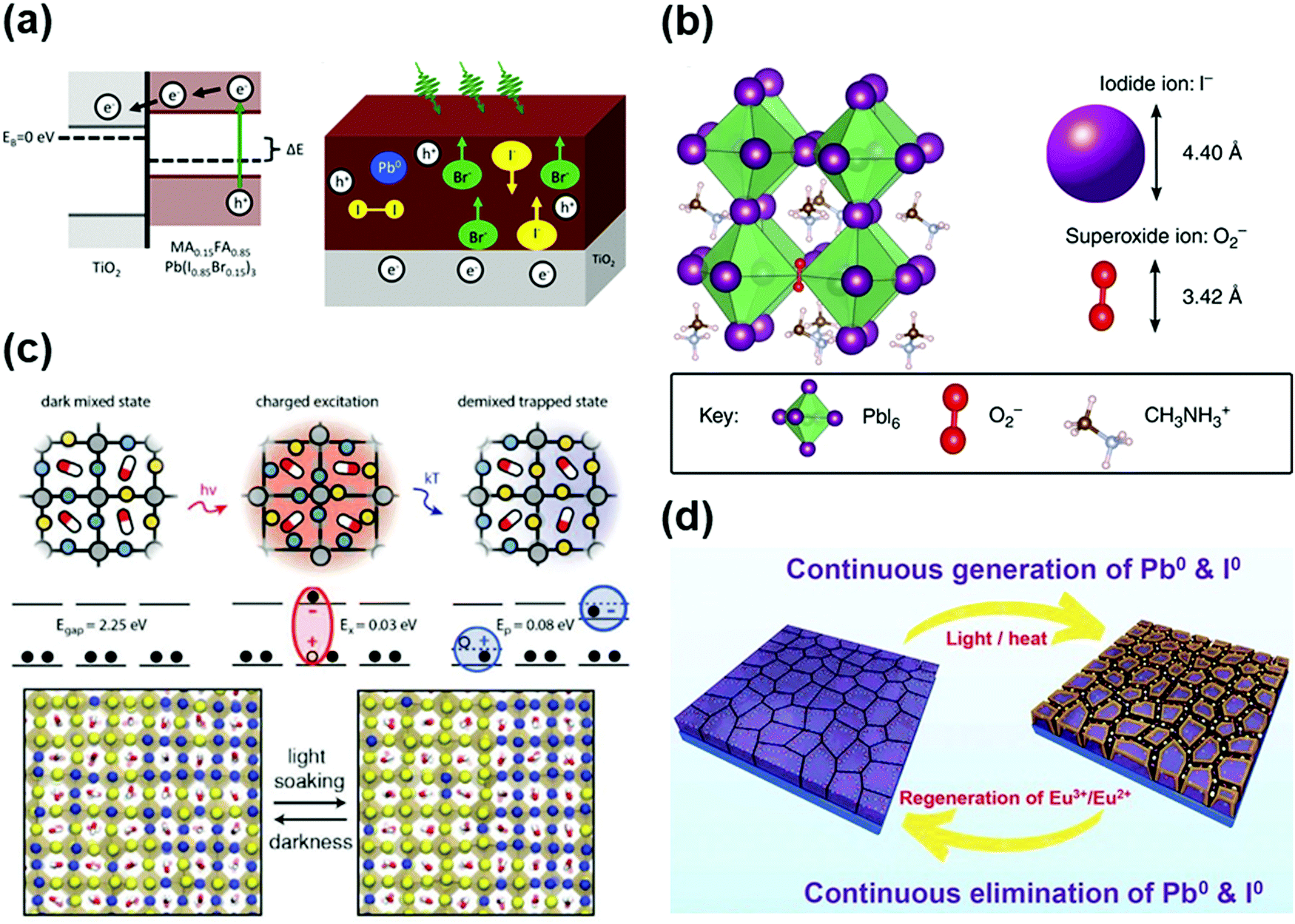 | ||
| Fig. 8 (a) (left) Illumination leads to charge separation to the substrate and a change in the Fermi level. (right) Schematic image of the composition changes in the perovskite film under illumination: Pb0 and I2 are formed. The surface becomes more halide rich. Br− moves to the surface. Reproduced with permission from ref. 169. Copyright 2017, American Chemical Society. (b) (left) Atomic structure of CH3NH3PbI3 showing superoxide ion, O2, occupying an iodide vacancy, VxI (for clarity, a pseudo-cubic sub region of the structure is shown and not the full tetragonal supercell used in the calculations). (right) Comparison of relative size of iodide and superoxide anions (using ionic radius of I, and for the superoxide ion, interpolation between the covalent radius of O2 and ionic radius of O2). Reproduced with permission from ref. 137. Copyright 2017, Nature. (c) Schematic of phase separation and reversibility in MAPb(IxBr1−x)3, where yellow and blue spheres represent I− and Br−, respectively, the red and white pill shapes represent MA, and the lead atoms (not shown) are located in the center of the octahedra. Photoinduced polaron trapping and associated energy scales associated with phase separation. Reproduced with permission from ref. 174. Copyright 2017, American Chemical Society. (d) Schematic of the ability of Eu2+–Eu3+ ion pairs to eliminate Pb0 and I0 defects. Reproduced with permission from ref. 184. Copyright 2019, Science. | ||
(2) Ion migration and phase segregation are correlated with the migration of halide vacancies under early-stage (∼101–2 seconds) and longer-term (∼hours) illumination, respectively, which influence the A-site cation distribution. For instance, deQuilettes et al. demonstrated that an increase in photoluminescence intensity in MAPbI3 films over a timescale of ∼101 min under illumination is correlated with the migration of I− species away from the illuminated area and the presence of point defects, particularly halide vacancies.172 Hoke et al. also reported that APb(BryI1−y)3 perovskites could undergo reversible phase segregation into Br−- and I−-rich phases under light exposure.173 Bischak et al. proposed that the photoinduced phase separation in mixed halide hybrid perovskites could be mediated through strain-induced phase separation at the regions with photogenerated polarons and their accompanying lattice distortions (Fig. 8c).174 The lattice could be deformed through interactions among the highly concentrated carriers and the highly soft ionic lattice, as illustrated in Fig. 8b.137 In addition to the light-induced halide segregation, Christians et al. demonstrated that the Cs+, FA+ and MA+ cations could be redistributed throughout the film within hours of illumination.158
Similarly, carrier transport materials also suffer from photo-instability. It was reported that photo-excited dimerization could create disorder and inhibit charge migration in fullerene-based ETMs.175 Besides, TiO2-based devices showed a rapid decay in open circuit voltage and photocurrent within hours of UV light exposure under inert conditions, given that the degradation pathway induces rapid recombination across the TiO2–perovskite interface.
Furthermore, oxygen and light impose coupling effects on the stability of materials and devices. Oxygen, upon illumination, mainly interrupts the ETMs and perovskite absorbers in the devices. Aristidou et al. suggested that molecular oxygen reversibly adsorbed and diffused through iodide vacancies, whereby they created a trap state near the conduction band.137 The charged O2− superoxide is formed when the perovskite is in the excited state, which initiates an acid–base reaction with the MA+ cation by deprotonation into water molecules, iodine, lead iodide, and methylamine vapor.
Some useful strategies have been developed to improve the intrinsic photostability and/or photooxidation stability of ETMs, HTMs and perovskite absorbers. For ETMs, replacing TiO2 with SnO2, Al2O3 or fullerene and implementing a UV filter have been demonstrated and considered to be effective means to mitigate the photo-oxidation.158,176 Zhao et al. fabricated a thick fullerene-decorated TiO2 backbone film directly on top of a perovskite film through a simple room temperature solution process in PSCs with an inverted configuration. The fullerene-decorated TiO2-based device with encapsulation retained ∼90% of its initial PCE (18.1% vs. 20.3%) after 350 h MPP tracking test under ambient conditions at ∼30 °C and 50% ± 5% RH, owing to the passivation and filling of the fullerene mixture.177 For HTLs, Yang et al. synthesized In-doped CuCrO2 nanoparticles (NPs) and fabricated them into HTM layers, whereby the device retained 90% of its initial PCE after 800 h of continuous radiation without encapsulation in a glovebox.178 Besides, Li et al. utilized CsBr as a TiO2–perovskite interface modifier that can inhibit the photocatalytic activity of TiO2, which effectively improved the UV resistance.179 Ito et al. reported that the introduction of Sb2S3 at the TiO2–CH3NH3PbI3 interface could stabilize the interface against light exposure.180 Gao et al. introduced an inorganic salt, potassium thiocyanate (KSCN), as an interface layer between NiOx (as HTL) and MAPbI3 through a cross-linking interaction. They found that the unencapsulated NiOx/KSCN-based device showed only 11% decay in PCE, whereas the device without KSCN lost 67% of its initial efficiency.181 Furthermore, Bella et al. demonstrated the employment of a down-converting fluoropolymer that can convert the incoming UV light into visible light, deactivating the photoexcitation of TiO2 layer, leading to improved UV irradiation stability.182 Ma et al. developed a novel strategy by synthesizing perovskite-coated PbS quantum dots (QDs) and fabricating them as the interface layer. The strong interactions of PbS QDs with perovskites could simultaneously immobilize the iodide ions and reduce the dangling bond of the Pb cation at the perovskite-HTM interface. After 400 h continuous illumination in the ambient environment at 25 °C, 65–70% RH, the encapsulated PSCs coated with PbS QDs maintained 85% of their initial PCE, while the control device only maintained 54% of its initial performance.183
(3) For the perovskite layer itself, Saidaminov et al. proposed that the incorporation of Cd into the CsMAFA-based perovskite lattice could release the local strain and maximize the formation energy of defect, which is responsible for degradation, leading to prolonged lifetime by one order of magnitude at maximum power point operation in ambient air (50% RH).142 To solve the instability induced by the formation of Pb0 and I0 species, Wang et al. demonstrated a novel strategy, employing the europium (Eu) ion pair Eu3+–Eu2+ as a “redox shuttle”, which can simultaneously selectively oxidized Pb0 (by Eu3+ → Eu2+) and reduce I0 (by Eu2+ → Eu3+) defects (Fig. 8d), ensuring high stability to retain 92% of the peak PCE under 1 sun continuous illumination and 91% of the original stable PCE after maximum power point tracking for 500 h, respectively.184 Li et al., using an antisolvent process for tuning the perovskite nucleation and crystal growth, obtained a heterojunction quasi-core–shell perovskite structure with Pb–Sn perovskite wrapped in a tin(II) complex. Remarkably, the device lifetime was significantly extended by over 18.5-folds from 30 to 560 h under continuous light illumination, owing to the protection of the quasi-core–shell structure.23 Wang et al. fabricated CsPbI3 decorated with 4-aminobenzoic acid (ABA), followed by treatment with steric neostigmine bromide (NGBr) to further mediate the thin film surface (NGBr–CsPbI3(ABA)). They proposed that the ABA or NG cation adsorbed on the grain boundaries or the surface of CsPbI3 could immobilize the PbI6 octahedra by pulling up the energy barriers for their rotation. The NGBr–CsPbI3(ABA)-based devices retained 90% of their initial PCE after 500 h continuous white light illumination, compared with the 50% decline for the CsPbI3-based PSCs.22
Besides, 2D-, quasi-2D and mixed 2D/3D structures display impressive photostability, owing to their large cations, which can suppress ion diffusion, vacancy migration and accumulation (Fig. 9a and b).156,185–188 Tsai et al. discovered that Ruddlesden–Popper layered perovskites preferentially adopt an out-of-plane alignment to the planar contacts in solar cells to facilitate charge transport (Fig. 9a).185 Some perovskite systems have been demonstrated to have superior stability under continuous illumination for up to ∼103 h, such as FA0.83Cs0.17Pb(I0.83Br0.17)3, FA0.7MA0.25Cs0.05PbI3, and FA0.83Cs0.17PbI2.7Br0.3, due to the regulation of their structural stability and the inhibited acid–base reaction between the superoxide and A-site cation species.168,189–191
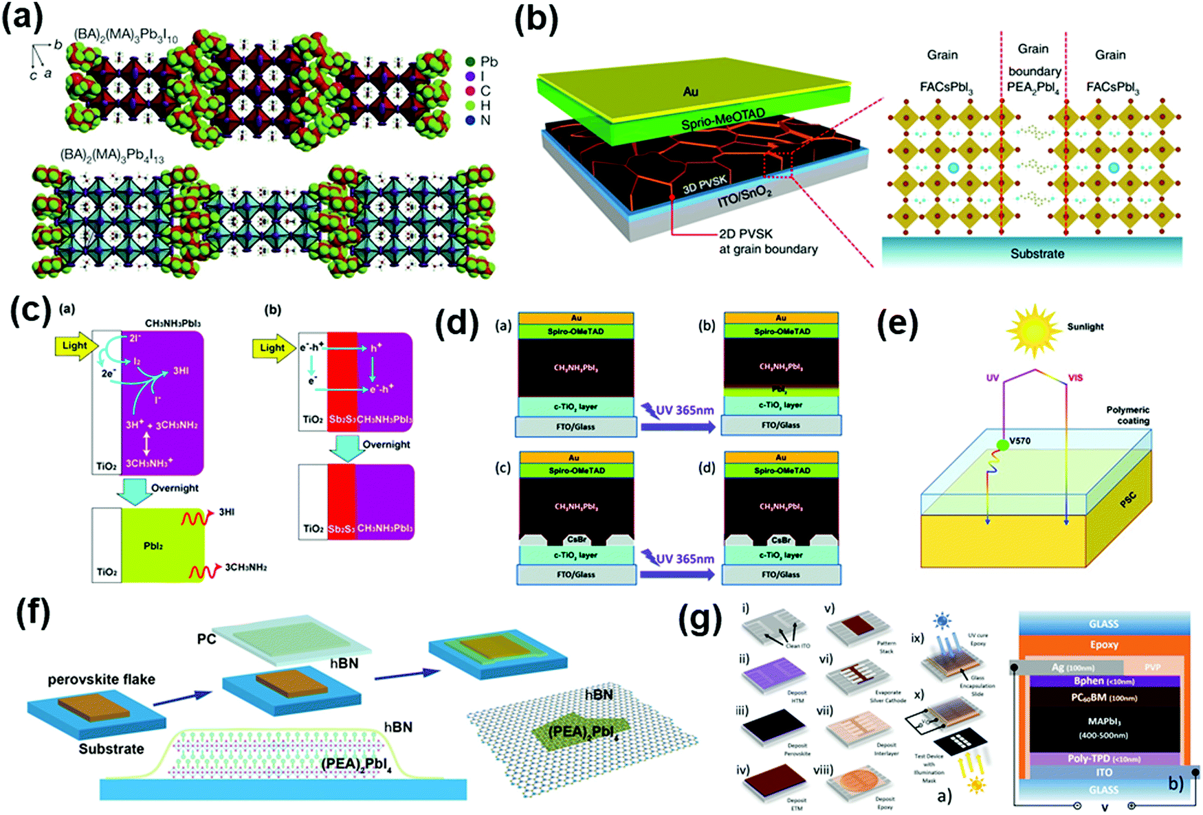 | ||
| Fig. 9 (a) The crystal structure of the Ruddlesden–Popper (BA)2(MA)2Pb3I10 and (BA)2(MA)3Pb4I13 layered perovskites, depicted as n polyhedral blocks, where n refers to the number of layers; the BA spacer layers are depicted as space-fill models to illustrate the termination of the perovskite layers. Reproduced with permission from ref. 185. Copyright 2016, Nature. (b) Schematic of the device incorporating polycrystalline 3D perovskite film with 2D perovskite at the grain boundaries. Reproduced with permission from ref. 188. Copyright 2018, Nature. (c) Degradation scheme of CH3NH3PbI3 perovskite solar cells during the light exposure test: (a) 〈TiO2/CH3NH3PbI3〉 and (b) 〈TiO2/Sb2S3/CH3NH3PbI3〉. Reproduced with permission from ref. 180. Copyright 2014, American Chemical Society. (d) Schematic illustration of the control perovskite solar cell (a) before and (b) after UV irradiation, and perovskite solar cell with CsBr interface modification (c) before and (d) after UV irradiation. Reproduced with permission from ref. 179. Copyright 2016, Royal Society of Chemistry. (e) Scheme of the UV-coating operating principle. Reproduced with permission from ref. 98. Copyright 2016, Science. (f) Schematic of the hBN-perovskite stack fabrication process for the encapsulation of perovskite nanoflakes. Reproduced with permission from ref. 108. Copyright 2018, Wiley-VCH. (g) (a) A schematic of the fabrication and testing routine used to create perovskite solar cells incorporating PVP/epoxy encapsulation and (b) device architecture showing all layers, together with their approximate thicknesses. Reproduced with permission from ref. 93. Copyright 2018, Wiley-VCH. | ||
Improving the intrinsic stability of materials and device stacks is critical to reduce photo-oxygen coupling. As previously mentioned, the 2D flakes, Sb2S3 (Fig. 9c) and CsBr (Fig. 9d), and a down-converting fluoropolymer were employed in the perovskite grain boundary and TiO2 upper interface to enhance the resistance to photo-oxygen especially under UV light, which could also be used for the functional selection of encapsulation materials at the grain boundary and interface (Fig. 9e).108,179,180,188 Besides, there were also reports about other interface encapsulation and external encapsulation to improve the photostability and/or photooxidation stability by inhibiting ion migration and water/oxygen intrusion. For perovskite/HTL (hole transport layer) interface encapsulation, Fang et al. discovered that the degradation of the 2D perovskite (PEA)2PbI4 initiated at the crystal edges and surface. They proposed that the light-induced degradation could be suppressed by interface encapsulation using hexagonal boron nitride (hBN) flakes and/or polycarbonates (Fig. 9f).108 Bella et al. showed that a multifunctional fluorinated photopolymer coated on the perovskite film acted as a strongly hydrophobic barrier against environmental moisture, resulting in a prolonged lifetime for more than 6 months under UV irradiation.98 For the HTL/electrode interface, Arora et al. demonstrated that the addition of a conductive reduced graphene oxide (rGO) spacer layer between CuSCN and gold could enable >95% retention of the initial efficiency after ageing at a maximum power point for 1000 h. This can be ascribed to the inhibited electrical potential-induced reaction of gold with the thiocyanate anions.192 Besides, tin oxide, Al2O3 nanoparticles and Cr metal interlayer were also used as interface encapsulation to avoid the migration of the electrode metal through the hole transporting layer to the perovskite.190,193 For external encapsulation, encapsulation systems containing PVP and epoxy, nonpolar paraffin and epoxy, as previously mentioned, could all achieve 80% of their initial PCE after 1000 h of AM1.5 irradiation and continuous maximum power point output (Fig. 9g).93
3.4 Stability against thermal treatment
(1) The structural stability of the ABX3 perovskite lattice, which can be assessed by the Goldschmidt tolerance factor (t) and supposed to be in the range of 0.71–1 as a stable lattice, can induce the most intrinsic instability issue. The phase would transform from photoactive to non-photoactive phases (i.e., α to δ) when the temperature decreases to room temperature for FA- and Cs-based perovskites due to the inappropriate sizes of their A-site cations. The MA-based perovskites can form photoactive structures at room temperature, but will undergo phase transformation from a tetragonal phase to cubic phase (α to β) at ∼55 °C.
(2) Halide perovskites usually undergo ion migration and undesirable aggregation upon heating. McKenna et al., using epifluorescence microscopy (FM), revealed the deteriorated quality of a CH3NH3PbI3−xClx film under prolonged thermal treatment at 60 °C (Fig. 10a).101 The quenching of the fluorescence after ∼101–2 h was attributed to the grain aggregation and the formation of non-radiative trap sites in the films. Matsui et al. carried out elemental analysis on the perovskite films before and after heat treatment at 85 °C for 1000 h. The time-of-flight secondary ion mass spectrometry (TOF-SIMS) and energy-dispersive X-ray spectrometry (EDX) showed that micrometer-scale aggregates containing Rb and Br were formed after thermal stress testing (Fig. 10b and c, respectively).194
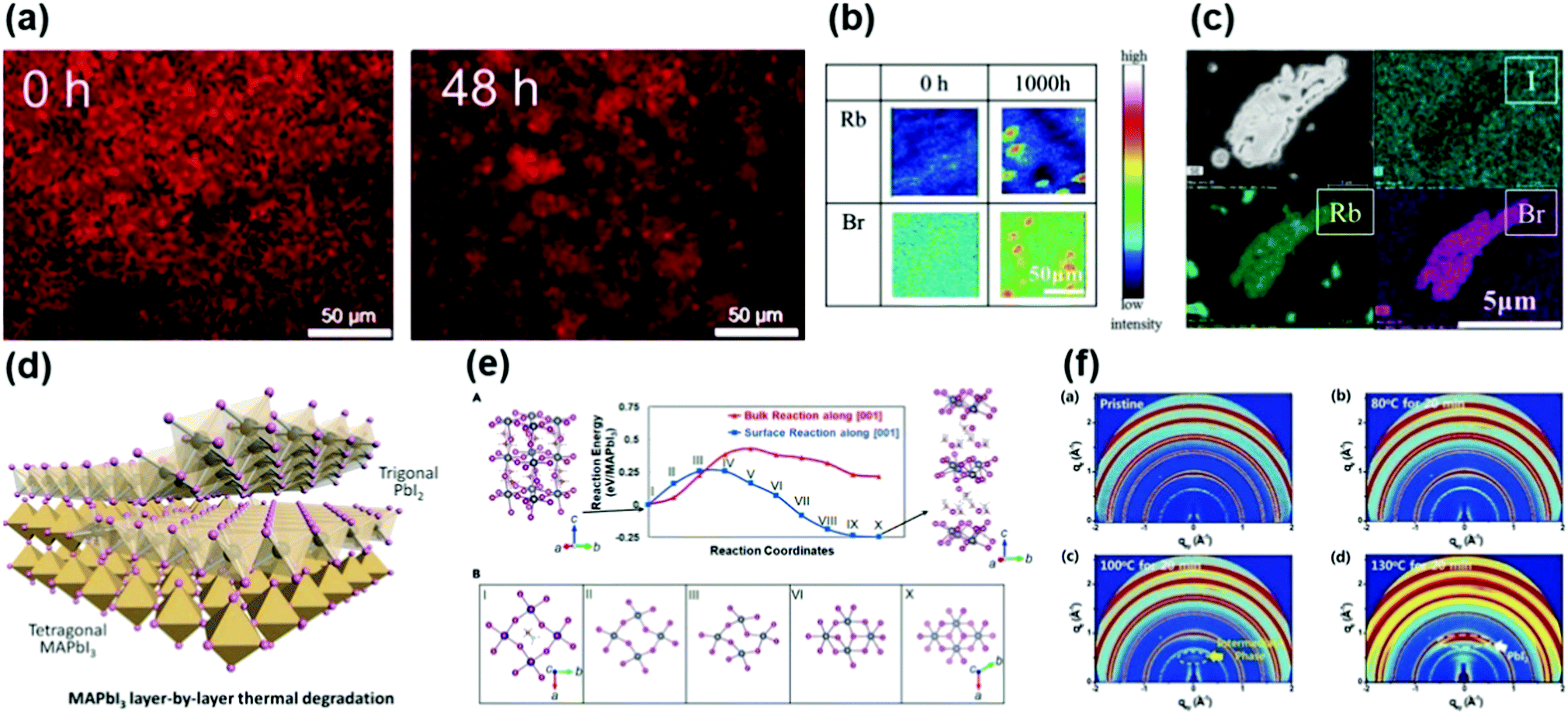 | ||
| Fig. 10 (a) Thermal degradation of polymer-encapsulated CH3NH3PbI3−xClx films at 60 °C as a function of time monitored by fluorescence microscopy. CH3NH3PbI3−xClx degradation is accompanied by a decrease in emission intensity, and hence darkening of the image occurs. Reproduced with permission from ref. 101. Copyright 2017, Royal Society of Chemistry. (b) Top-view TOF-SIMS elemental mapping of the perovskite film before and after a thermal stress test at 85 °C for 1000 h. The composition of the perovskite film is Rb0.05Cs0.05FA0.75MA0.15Pb(I0.83Br0.17)3. Reproduced with permission from ref. 194. Copyright 2019, Wiley-VCH. (c) SEM image of the agglomeration (top left), EDX elemental mapping of I (top right), Rb (bottom left), and Br (bottom right). Reproduced with permission from ref. 194. Copyright 2019, Wiley-VCH. (d) MAPbI3 layer-by-layer thermal degradation. Reproduced with permission from ref. 195. Copyright 2017, Elsevier Inc. (e) The reaction energy profiles calculated using the ssNEB method. The saddle point is 0.26 eV for surface degradation and 0.43 eV for bulk degradation along the [001] axis. Selected transition states of an individual PbI2 layer during the surface reaction. The evolution of the structure shows contraction of the MAPbI3 layer along the a-axis ([100] direction) to form a PbI2 layer. Reproduced with permission from ref. 195. Copyright 2017, Elsevier Inc. (f) In situ 2D GIWAXD patterns of MAPbI3 perovskite films determined under different thermal conditions. (a) Pristine MAPbI3, and MAPbI3 exposed to (b) 80 °C for 20 min, (c) 100 °C for 20 min, and (d) 130 °C for 20 min. Reproduced with permission from ref. 196. Copyright 2017, Nature. | ||
(3) The thermally activated chemical reaction results in the formation of unwanted species in perovskite films. Using in situ TEM, Fan et al. found that the crystalline structure gradually transformed from tetragonal MAPbI3 to trigonal PbI2 through a fixed surface-initiated layer-by-layer degradation pathway (Fig. 10d and e).195 The comprehensive characterization using in situ grazing-incidence wide-angle X-ray diffraction (GIWAXD) and high-resolution X-ray photoelectron spectroscopy (HR-XPS) carried out by Kim et al. confirmed that the MAPbI3 perovskite film decomposed into CH3I, NH3, and PbI2 after either short (20 min) exposure to heat stress at 100 °C or extended exposure (>1 hour) at 80 °C (Fig. 10f).196
(4) In addition to perovskite films, other functional layers in photovoltaic devices further complicate the thermal degradation processes in these devices. Spiro-OMeTAD, which is commonly used in high-efficiency PSCs, can crystallize within ∼101 h at 100 °C, and then the tBP (4-tert-butylpyridine) additive evaporates at a temperature as low as 85 °C, eventually forming voids at 80 °C in about 1 h. Besides, the metal electrode materials can react with halides due to the agitated diffusion of metal or halides at elevated temperatures.
To improve intrinsic structural stability against thermal decomposition, regulation of the perovskite composition and adopting thermally stable transport layers and electrode layer materials seem to be the most direct method. For instance, Niu et al. systematically studied the thermal stability of CsxMA1−xPbI3-based films and solar cells fabricated via a one-step spin-coating method. They found that the thermal stability of the CsxMA1−xPbI3 film was optimal when x = 0.09, which is superior to the pure MAPbI3, consistent with the trend of the device stability.197 Matsui et al. carried out a systematic investigation on the thermal stability of perovskite composition. They found that Rb can suppress the growth of PbI2 even under PbI2-rich conditions and decreasing the Br ratio in the perovskite absorber layer can prevent the generation of unwanted RbBr-based aggregates. The optimized device obtained by regulating the perovskite composition exhibited 92% PCE retention after the stress test at 85 °C/85% RH.194 Jung et al. fabricated PSCs using low-temperature solution-processed CuSCN as the inorganic HTM, which possessed a highly stable crystalline structure and was robust even at high temperature. Compared with spiro-OMeTAD-based PSCs retaining only 25% of their initial PCE after annealing for 2 h at 125 °C in air with 40% RH, the CuSCN-based PSCs maintained approximately 60% of their initial PCE, exhibiting superior thermal stability under identical conditions.198 Baranwal et al. fabricated three-layer printable HTM-free MAPbI3 solar cells with a mesoporous carbon back contact. The devices survived with a lifetime of over 1500 h at 100 °C in the thermal stability test.199 However, encapsulation is still vital to further improve the structure stability of perovskite by blocking the escaping pathway of organic and halide species. It also prevents ion migration and metal-induced degradation from occurring during thermal treatment. Some more reports on improving the thermal stability through a systematic encapsulation concept are briefly introduced and discussed as follows.31,97,101,107,109,195,200
Grain boundary encapsulation has been found to be effective in improving the intrinsic stability of perovskites. Liu et al. found that the amorphous silica formed in situ at the nanoscale grain boundaries slowed down the phase transformation kinetics of α-phase FA0.85Cs0.15PbI3 to non-perovskite δ-phase, as suggested by density functional theory (DFT) calculations, and hence improved the intrinsic stability of the perovskite grains (Fig. 11a).107 Lin et al. proposed that the intrinsic stability of the perovskite films and devices could be improved through the incorporation of (BA)2PbI4 layers on the surface and/or at the grain boundaries of 3D MAPbI3 (Fig. 11b).109 Based on the capacitance-frequency measurements, the 2D/3D stacking structures could effectively reduce the defect density, suppress ion migration and prevent the escape of the cationic and halide components on the surface and at grain boundaries.
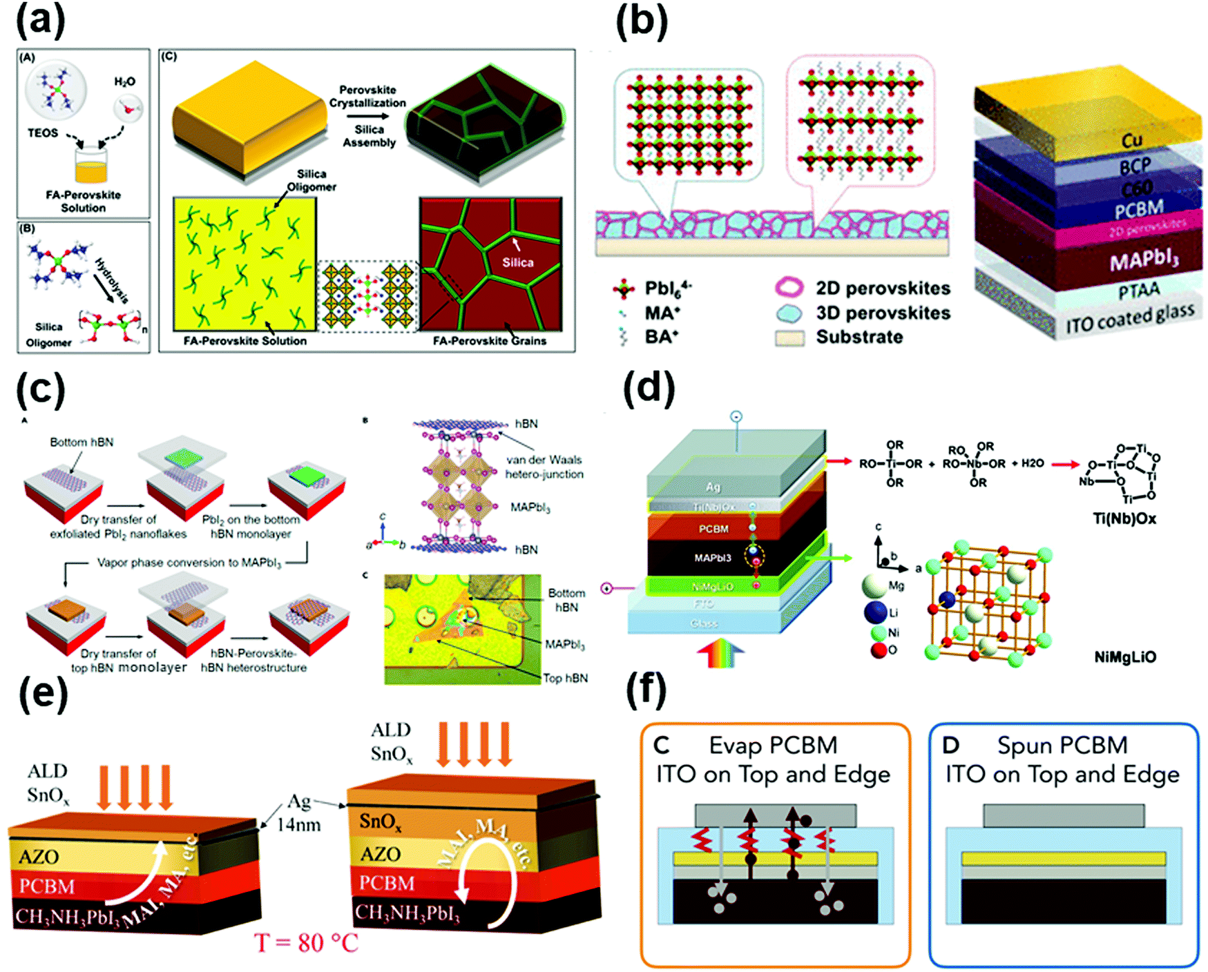 | ||
| Fig. 11 (a) Schematic illustration showing (A) the mixing of the FA-based perovskite precursor solution and the silica precursors in “one pot”, (B) the formation of silica oligomers via the hydrolysis reaction of TEOS with water, and (C) the formation process of the FA-based perovskite film consisting of individual silica-encapsulated grains from the silica-oligomer-containing precursor solution. Reproduced with permission from ref. 107. Copyright 2018, Wiley-VCH. (b) (left) Schematic figure of the perovskite film treated with BA to form a 2D/3D stacking structure. (right) Schematic figure of the device structure. Reproduced with permission from ref. 109. Copyright 2018, American Chemical Society. (c) (A) BN–perovskite–BN heterostructure fabrication process. (B) Schematic of the BN–perovskite–BN heterostructure. (C) The BN–perovskite–BN heterostructure on a gas cell bottom chip. Reproduced with permission from ref. 195. Copyright 2017, Elsevier Inc. (d) Diagram of the cell configuration highlighting the doped charge carrier extraction layers. The right panels show the composition of Ti(Nb)Ox and the crystal structure of Li+-doped NixMg1−xO, denoted as NiMg(Li)O. Reproduced with permission from ref. 201. Copyright 2015, Science. (e) Scheme of the capping process via ALD for AZO/Ag and AZO/SnOx/Ag samples. Reproduced with permission from ref. 97. Copyright 2017, Wiley-VCH. (f) Schematic of the barrier layers evaluated in this study showing the degradation mechanisms that occur with each design. Reproduced with permission from ref. 200. Copyright 2018, American Chemical Society. | ||
Surface encapsulation of the perovskite films can effectively improve the thermal stability and inhibit the decomposition of perovskites initiated at the surface. Fan et al. encapsulated an MAPbI3 film with thin flakes of hexagonal boron nitride (hBN) to form an hBN-perovskite-hBN heterostructure.195 It showed no obvious structural change after 30 min of continuous heating at 85 °C by restraining the structure transformation of the surface layer, in contrast to the rapid emergence of the trigonal phase in the non-encapsulated tetragonal perovskites within 1 min upon the same thermal treatment. The in situ TEM characterization and DFT calculation showed that the charges in hBN (B+ and N−) interacted with the dangling bonds (Pb+ and I−) to reduce the surface activity, leading to a 7-fold slower surface reaction rate, and improved the overall stability of the material (Fig. 11c).195 Chen et al. employed a heavily doped inorganic charge extraction layer in planar PSCs and achieved robust stability to sustain continued current flow under light exposure for 1000 h (Fig. 11d).201 McKenna et al. investigated several polymer encapsulants (poly(methylmethacrylate) (PMMA), ethyl cellulose (EC), polycarbonate and poly(4-methyl-1-pentene) (PC)) and their usability as barrier layers to improve the stability of CH3NH3PbI3−xClx films under prolonged thermal degradation at various temperatures. Compared to the EC- and PC-encapsulated perovskite films, the PMMA-encapsulated film showed invisible degradation to PbI2 after extended heating at 60 °C, which could be ascribed to its low water vapor transport rate (WVTR), appropriate glass transition temperature (Tg), low O2 permeability and hydrophobicity.101
Interface encapsulation of the perovskite device can prevent ion migration and metal-induced degradation from occurring during thermal treatment. Boyd et al. showed that a barrier layer and sealing at the edges of the active layers could be highly effective in preventing the possible reactions of perovskites with the metal contacts and inhibiting the escape of volatile species. Using ITO and PCBM to form full-coverage barrier layers, the PSCs achieved 1000 h thermal stability at 85 °C (Fig. 11f).200 Besides, Zhao et al., using the SnOx/Ag/SnOx sandwiched structure, demonstrated that the device almost did not degrade for over 4500 h at an elevated temperature of 60 °C (Fig. 11e).97
In addition to systematic encapsulation such as grain boundary, surface and interface encapsulation, the external encapsulation strategy is also applied to improve the thermal stability. Fu et al. compared the encapsulation effect of three different types of hot melt films (polyurethane, PU; polyolefin, POE; and ethylene vinyl acetate, EVA), and demonstrated that the PU-encapsulated printable PSCs and submodules showed significantly enhanced thermal stability due to the mild laminating temperature at 80 °C and the effective prevention of moisture intrusion.31
Similarly, the above-mentioned degradation mechanism caused by moisture, oxygen and heat also occurs in the device in damp-heat test (85 °C–85% RH). Besides, the strategies to improve the individual stability of devices under moisture, oxygen and heat have been elaborated in previous sections from two aspects, as follows: (1) intrinsic stability regulation of the material and device architecture and (2) encapsulation configuration. In this section, we further clarify the essential role of encapsulation in improving the device stability, targeting a harsher damp-heat test (85 °C–85% RH).
In 2015, Han et al. investigated the stability of encapsulated planar-structured MAPbI3 PSCs and revealed the degradation mechanism at high temperature and humidity (85 °C–80% RH). Although the WVTR was reduced with the use of a UV-curable epoxy adhesive (3035B) and desiccant, showing slightly improved stability, the encapsulated devices still suffered from MAPbI3 degradation into CH3NH2, HI and PbI2, wherein HI could react with the silver electrode (Fig. 12a).96 Subsequently, voids were formed in the perovskite and spiro-OMeTAD layer, leading to the detachment of the perovskite layer and TiO2 layer.96 Then, Bush et al. were the first to successfully demonstrate an encapsulated single-junction perovskite cell that could withstand a 1000 h damp heat test at 85 °C and 85% relative humidity. In this work, an ALD- or pulsed-CVD-processed SnO2/ZTO (zinc tin oxide) bilayer, together with a sputtered ITO layer, acted as the diffusion barrier layer to significantly increase the thermal and environmental stability.190 Bi et al. developed a low-temperature processing to fabricate low-dimensional diffusion barriers, which could reduce the unwanted interfacial ionic diffusion by 103–107 times, and thereby increase the operational stability of high-efficiency PSCs modules.202 They achieved 36 cm2 PSCs modules, retaining over 95% of their initial PCE (over 15%) after 1000 h of heating at 85 °C, and 91% after light soaking in AM 1.5G solar light for 1000 h, respectively (Fig. 12b).202
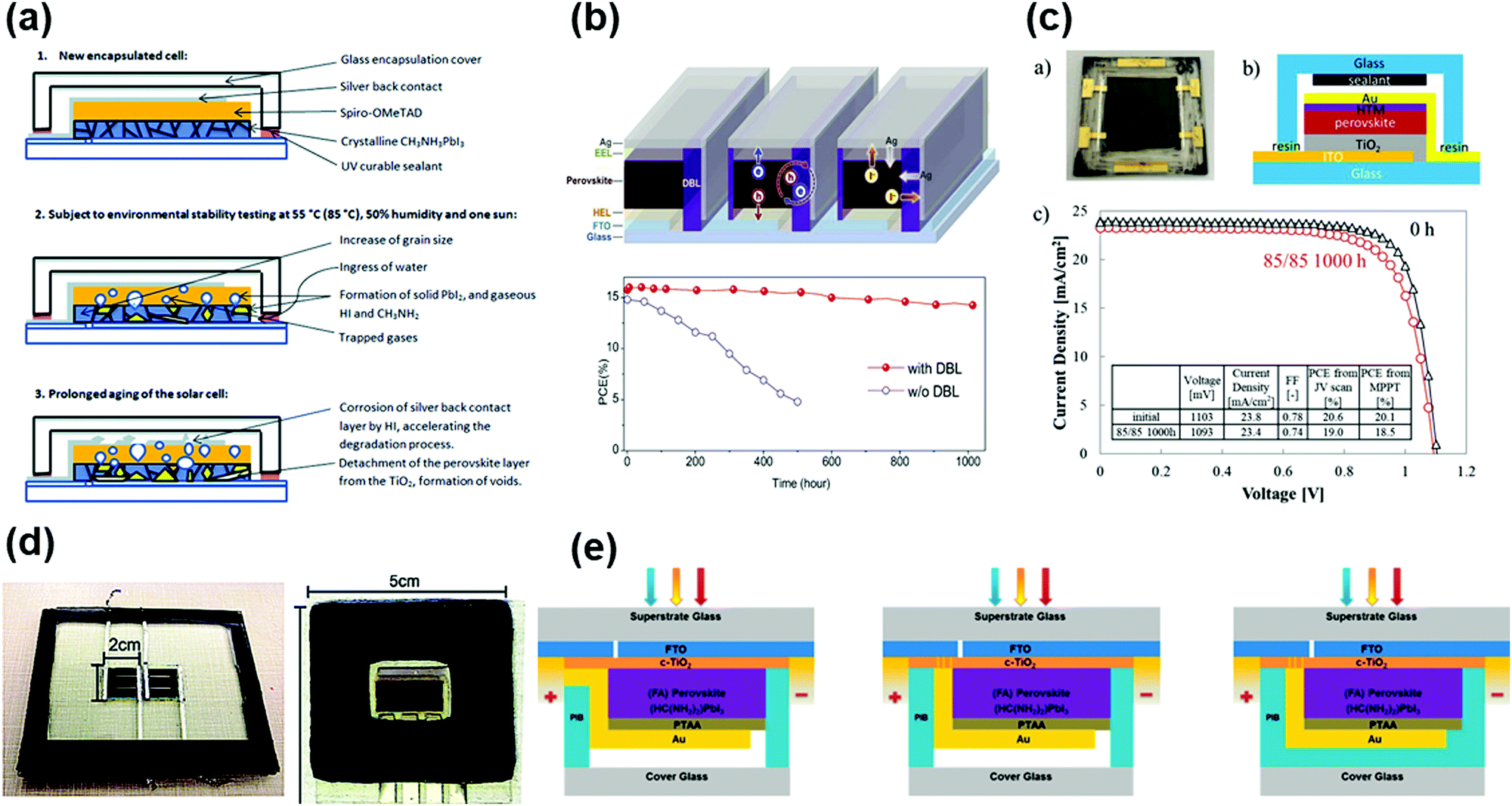 | ||
| Fig. 12 (a) Scheme of the degradation processes of encapsulated methylammonium lead iodide perovskite solar cells illuminated at elevated temperatures and high humidity. Reproduced with permission from ref. 96. Copyright 2015, Royal Society of Chemistry. (b) Illustration of the diffusion process and interfacial charge transfer (solid lines) and recombination (dotted circle) in PSC module (EEL is the electron extraction layer and HEL is the hole extraction layer) and heating ageing test at 85 °C with relative humidity of about 85% for 1000 h. Reproduced with permission from ref. 202. Copyright 2019, Elsevier Inc. (c) (a) Photograph of the encapsulated device and (b) cross-sectional structure of the encapsulated device. (c) J–V curve of the device with an optimized perovskite composition of Rb0.05Cs0.05FA0.75MA0.15Pb(I0.95Br0.05)3 before and after damp heat testing at 85 °C/85% RH for 1000 h under air mass (AM) 1.5G irradiation of 100 mW cm−2. Reproduced with permission from ref. 194. Copyright 2019, Wiley-VCH. (d) Top view image of (left) 1st generation and (right) 2nd generation package after lamination. Reproduced with permission from ref. 104. Copyright 2018, Royal Society of Chemistry. (e) Cross-sectional schematic from the FTO glass side of PSCs encapsulated by three methods (not to scale). In method 1, PIB is applied over a thin gold film, which is the positive electrical feedthrough for the cell. In methods 2 and 3, both electrical feedthroughs are provided by the FTO layer. Methods 1 and 2 use PIB as an edge seal, whereas in method 3, PIB blankets the entire area under the cover glass. Reproduced with permission from ref. 95. Copyright 2017, American Chemical Society. | ||
Similar to interface encapsulation, the diffusion barrier layer can trap the volatile byproducts and inhibit moisture intrusion. The stability could be further improved through industrial standard encapsulation such as EVA (ethylene-vinyl acetate) and glass.190 Subsequently, the same research group designed 2nd generation encapsulation technology to further improve the 85 °C–85% RH damp heat stability. The main optimization was achieved through the novel design of the electrical feedthrough and the widened edge seal, which could effectively reduce the moisture intrusion and cavity formation (Fig. 12d).104 In addition to these studies, Shi et al. also demonstrated that a polyisobutylene (PIB)-encapsulated device maintained its initial efficiency after 540 h of damp-heat testing. They emphasized that the feedthrough design and the prohibited residual space of the encapsulated device could resist the ingress of moisture and suppress the escape of gaseous products (Fig. 12e).95 Matsui et al., using a water-absorbing sealant for encapsulation, successfully obtained 92% PCE retention after 1000 hour 85 °C/85% RH damp-heat test (Fig. 12c).194
3.5 Thermal cycling (−40 to 85 °C) stability
Thermal stress is a detrimental ageing factor that can induce the decomposition of perovskites, micro-cracks in films, interface delamination, and even fracture, which can lead to device failure. Thermal stress can arise during the annealing process and temperature fluctuations in actual outdoor operating conditions. After a systematic comparison from the stress tests of perovskite films deposited on rigid and flexible substrates, Zhao et al. suggested that the residual strain generated during the annealing could be ascribed to the mismatch of the thermal expansion coefficients between the substrate and the perovskite material (Fig. 13a).103 Our group furthe observed the residual strain gradient in perovskite films was closely related to lattice structure evolution due to detectable compositional inhomogeneity, and discovered that the thermal strain may take effects due to the temperature gradient and the mismatch of the thermal expansion coefficients between the substrate and the perovskite during the annealing process.105 Rolston et al. reported that, in perovskite films, the tensile strain could sometimes exceed 50 MPa, which is high enough to deform copper, and hence act as a significant driving force to fracture the film (Fig. 13b).106 Through the DFT simulations, Tu et al. showed that tensile strain could aggravate the distortion of the inorganic [PbI6]4− octahedra and stretching of the Pb–I bond.203 Moreover, Zhao et al. confirmed that the existence of residual strain could lower the activation energy for ionic migration, leading to the degradation of perovskite, and hence instability (Fig. 13c).103 | ||
| Fig. 13 (a) (a) Without a substrate, the perovskite formed at 100 °C contracts vertically and laterally during cooling. (b) With the substrate adhesion, the annealed perovskite film only contracts vertically. Reproduced with permission from ref. 103. Copyright 2017, Science. (b) Photographs of MAPbI3 on PET with externally applied stresses ranging from −130 to 130 MPa after 24 h of damp air aging at 25 °C and 85% RH or dry heat aging at 85 °C and 25% RH, where applied compressive stress enhanced the film stability and applied tensile stress reduced the film stability. Reproduced with permission from ref. 106. Copyright Wiley-VCH. (c) Variation in the activation energy of ion migration versus strain in the MAPbI3 films. Reproduced from ref. 103 with permission from Science, Copyright 2017. (d) The measured average Gc and PCE values as a function of cation composition, showing the trade-off between reliability and efficiency. Reproduced with permission from ref. 204. Copyright 2018, Wiley-VCH. (e) The measured cohesion (Gc) and degradation rate as a function of solar cell active material, showing the correlation between mechanical integrity and long-term reliability. Reproduced with permission from ref. 204. Copyright 2018, Wiley-VCH. | ||
Some strategies have been demonstrated to reduce the residual strain in perovskite films, such as low temperature annealing, oil bath annealing, A-site cation alloying, utilization of flexible substrates, and application of highly expandable HTM (Fig. 13d).204 However, although the residual strain can be reduced to some extent using these strategies, the PSCs still suffer from delamination under outdoor operating conditions for two reasons, namely their low fracture energy and the mismatched thermal expansion coefficients (TEC) of the multiple layers films in the devices (Fig. 13e).30,204–207 To assess the robustness of the PSC devices to thermal fluctuations, temperature cycling tests (−40 to 85 °C), as suggested by the IEC 61646 thin film module reliability standards, have been employed to accelerate the mechanical phenomena such as component decomposition, microcracks, and fractures under thermal stress conditions. Currently, the design of encapsulation is considered as the main approach to further improve the resistance of PSCs to thermomechanical stress.
In 2017, Shi et al. first reported that a PIB-encapsulated device could retain 200 cycles of its initial PCE under the thermal cycling tests. In this work, a special design in the feedthrough and the prohibited residual space of the encapsulated device enabled effective water-resistance and suppressed the escape of the gaseous decomposition products and t-BP vapor.95 Recently, they investigated the signature volatile products from the decomposition of organic hybrid perovskites under thermal stress using gas chromatography–mass spectrometry (GC–MS) with a PIB-encapsulated device. The device survived more than 1800 h of damp heat test and 75 cycles of humidity freeze test, for the first time, exceeding the requirement of the IEC61215:2016 standard (Fig. 14a and b).208 Cheacharoen et al. reported that a device encapsulated in softer EVA could withstand temperature cycling by retaining over 90% of its initial PCE after 200 temperature cycles (Fig. 14c).104Fig. 14d presents a schematic of a single-junction, semi-transparent perovskite solar cell.190 The fracture energy, determined through double cantilever beam (DCB) measurement, signifies the mechanical strength of a thin film and can be used to identify the weakest layer, which is prone to delamination. This work showed that the fracture energy of the perovskite film increased by about four times when stacking with laminated EVA or Surlyn on the top. Meanwhile, EVA with a lower elastic moduli allowed plastic deformation by dissipating the strain during mechanical testing.30 Subsequently, Cheacharoen et al. further compared three types of commercial encapsulants, including EVA, Surlyn, and polyolefins, with different elastic moduli and chemical reactivity. The polyolefins not only showed chemical inertness with perovskite, but also had a low elastic modulus similar to EVA. Therefore, the polyolefin-encapsulated device was demonstrated to withstand 200 thermal cycle tests.104 These efforts show that an appropriate elastic modulus and moisture resistance of the encapsulant are essential for encapsulated PSCs to pass the IEC 61646 temperature cycling test.
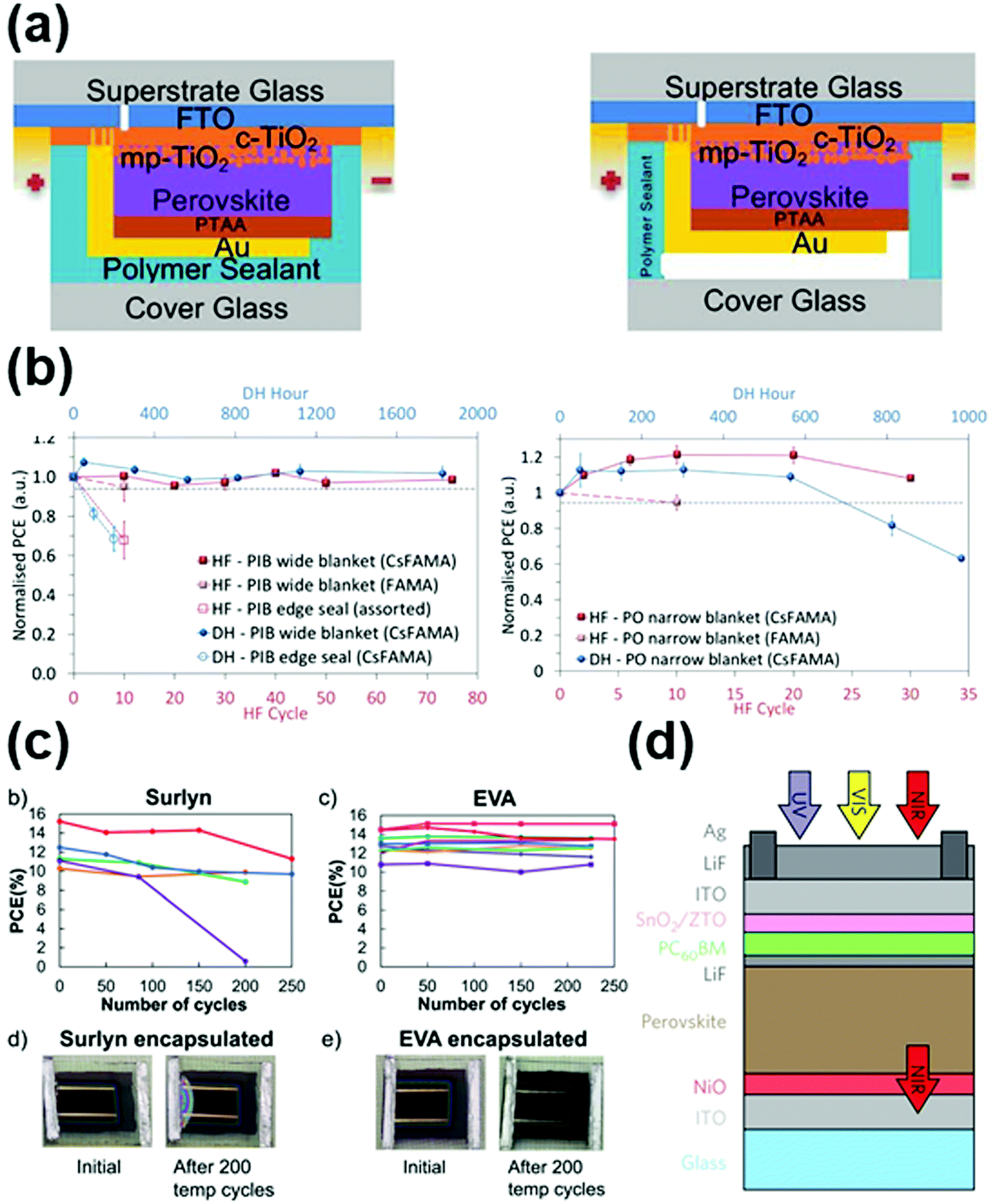 | ||
| Fig. 14 (a) Illustrations of the cross sections of the respective encapsulation schemes (not to scale). Reproduced with permission from ref. 208. Copyright 2020, Science. (b) Results of the IEC61215:2016 tests demonstrating the effectiveness of the packaging schemes. PCE evolution of (left) PIB-encapsulated or edge-sealed PSCs and (right) PO-encapsulated PSCs during the DH test and HF test. The dashed lines denote 5% relative PCE loss, which is the maximum allowed by the IEC standard after 1000 h of DH or 10 cycles of HF. Reproduced with permission from ref. 208. Copyright 2020, Science. (c) Power conversion efficiency of solar cells during temperature cycling packaged using (b) ionomer Surlyn PV5400 with five solar cells in the dataset and (c) ethylene vinyl acetate (EVA) with nine solar cells in the data set. Picture of the encapsulated solar cell before and after 200 temperature cycles in (d) Surlyn and (e) EVA. Reproduced with permission from ref. 30. Copyright 2018, Royal Society of Chemistry. (d) Schematic of a single-junction, semi-transparent perovskite solar cell (not to scale). Reproduced with permission from ref. 190. Copyright 2017, Nature. | ||
3.6 Initiative to quantitative encapsulation studies
In this section, we elaborate the diverse encapsulation strategies possibly used for PSCs to avoid the leakage of lead and improve their moisture and oxygen stability, photostability, thermal stability, damp-heat stability, and thermal cycling stability. These encapsulation strategies can be referred to as systematic encapsulation, including device external encapsulation and internal encapsulation. Device external encapsulation is mainly referred to as curable adhesive encapsulation and glass–glass vacuum laminated encapsulation; meanwhile, device internal encapsulation is mainly accomplished via grain boundary encapsulation, surface and interface encapsulation.Based on the systematic encapsulation, a large amount of research has been conducted on the stability of encapsulated devices. For device external encapsulation, by encapsulation with ethylene vinyl acetate (EVA), glass, and a butyl rubber edge seal, the solar cells could withstand the damp-heat test (85 °C/85% RH) for 1000 h with less than 10% performance degradation. When encapsulated in the softer EVA, the PSCs could withstand the temperature cycling test (−40 to 85 °C) and retained over 90% of their initial performance after 200 temperature cycles.30 The submodules (substrate area: 100 cm2) encapsulated with polyurethane (PU) maintained 97.52% of their initial efficiency after 2136 h under outdoor conditions (−10 to 70 °C).31 Recently, our group reported PSCs encapsulated by nonpolar paraffin to achieve a 1000 h operational lifetime at continuous maximum power point output in the ambient environment.32
For device internal encapsulation, Liu et al. found that the amorphous silica formed in situ at the nanoscale grain boundaries slowed down the phase transformation kinetics of FA0.85Cs0.15PbI3 from perovskite (α-phase) to non-perovskite (δ-phase), as suggested by DFT calculations, and improved the intrinsic or thermodynamic stability of the perovskite grains.107 Lin et al. reported that the thermodynamic stability of perovskite films and devices could be improved through the incorporation of (BA)2PbI4 layers on the surface and/or at the grain boundaries of 3D MAPbI3.109 Fang et al. reported that the light-induced degradation of the 2D perovskite (PEA)2PbI4 could be suppressed by encapsulation using hexagonal boron nitride (hBN) flakes and/or polycarbonates.108 Barry McKenna et al. utilized several polymer encapsulants, including (poly(methylmethacrylate) (PMMA), ethyl cellulose, polycarbonate and poly(4-methyl-1-pentene)), as barrier layers to improve the stability of MAPbI3−xClx films.101 Lee et al. developed a new method to integrate thin-film encapsulation (Al2O3 inorganic and pV3D3 organic multilayer) directly onto PSCs to enhance the device stability against moisture. The PSCs maintained 97% of their initial PCE after exposure to 50 °C and 50% RH for 300 h.94
Although encouraging progress has been made on the encapsulation of PSCs, quantitative investigations on the encapsulation mechanisms, operational principles and ageing test criteria are very limited. Therefore, it is challenging to make a fair comparison among different results to select the best and most appropriate encapsulation strategy. Here, we attempt to revisit the reported encapsulation results from two aspects. On the one hand, the results from the current research work carried out on systematic encapsulation are summarized in detail. On the other hand, we further advocate the establishment of standard and consistent procedures for the testing of encapsulation materials and stability of encapsulated devices. Regarding the systematic encapsulation, we list publications by focusing on three types of traditional encapsulation approaches in the field of PSCs, namely single-layer or multi-layer hydrophobic thin film encapsulation, curable adhesive encapsulation, and glass–glass vacuum lamination encapsulation. A detailed comparison can be found in Tables 1–3. Overall, glass–glass vacuum lamination encapsulation not only can prevent moisture and oxygen intrusion but also improve the photostability, thermal stability, damp-heat stability, and thermal cycling stability. Meanwhile, the potential of curable adhesive encapsulation to solve these stability issues seems to be lower than that of glass–glass vacuum lamination encapsulation, and single-layer or multi-layer hydrophobic thin film encapsulation can be considered as an internal encapsulation due to its limited ability to prevent moisture and oxygen intrusion.
| Encapsulation approaches | Device architecture | Encapsulation materials | Encapsulation procedure | Performance upon encapsulation | Ref. |
|---|---|---|---|---|---|
| Single-layer or multi-layer hydrophobic thin film encapsulation | FTO/TiO2/perovskite + Al2O3/spiro-OMeTAD + Al2O3/Au | Al2O3 | Mesoporous Al2O3 scaffold deposited by spin coating colloidal dispersion of 20 wt% Al2O3 (<50 nm) nanoparticles in isopropanol. | • Decay by 5% in PCE. | 193 |
| • 350 h in AM 1.5G illumination. | |||||
| ITO/PEDOT:PSS/CH3NH3PbI3/PCBM/AZO/SnOx/Ag/SnOx | SnOx | Ultrathin Ag layer deposited between SnOx layers by low-temperature atomic layer deposition (ALD). | • Decay less than 20% in PCE. | 97 | |
| • Over 4500 h at ambient atmosphere or 60 °C. | |||||
| MAPbBr3/AVA(MAPbBr3)2/Al2O3 | Bifunctional 5-aminovaleric acid (AVA), Al2O3 | 1. Formation of 2D/3D structure in into the MAPbBr3 layer by AVA crosslinking. | • No apparent damage to the Al2O3-coated AVA(MAPbBr3)2 films. | 209 | |
| 2. Al2O3 layer deposition (ALD, 15 nm) on the AVA(MAPbBr3)2 film. | • 3 min immersion in water. | ||||
| FTO/bl-TiO2/mp-TiO2/(FAPbI3)0.87(MAPbBr3)0.13/PTAA/Au | Al2O3 inorganic layers, pV3D3 organic layers | Multilayer stack of organic/inorganic layers deposited by initiated chemical vapor deposition and atomic layer deposition, respectively. | • Maintained 97% of initial efficiency. | 94 | |
| • 300 h exposure to 50 °C and 50% RH. | |||||
| Single-layer or multi-layer hydrophobic thin film encapsulation | FTO/TiO2/MAPbI3/carbon | Polydimethylsiloxane (PDMS) | PDMS dropped on top of the PSCs and baked at 80 °C until the total solidification of PDMS. | • No PCE drop. | 157 |
| • 3000 h at room temperature in the dark. | |||||
| CH3NH3PbI3−xClx/encapsulation film | Poly(methylmethacrylate) (PMMA), ethyl cellulose, polycarbonate, poly(4-methyl-1-pentene) | Spin-coating of PMMA (560 mg in 4 mL toluene (16.1 wt%)) and PMP (100 mg in 4 mL cyclohexane (3.2 wt%)) films. | • Extending the lifetime of the CH3NH3PbI3−xClx films from 24 h to >400 h. | 101 | |
| • Continuous heating at 60 °C. | |||||
| ITO/SnO2/perovskite/spiro-OMeTAD/Au | Thermosetting polyurethane (PU) | The encapsulant thickness controlled by the amount of precursor mixture and drop-casted onto the devices. | • Retaining more than 90% of initial efficiency. | 210 | |
| • Over 2500 h stored in ambient condition. |
| Encapsulation approaches | Device architecture | Encapsulation materials | Encapsulation procedure | Performance upon encapsulation | Ref. |
|---|---|---|---|---|---|
| Curable adhesive encapsulation | FTO/TiO2/MAPbI3/spiro-OMeTAD/Ag | Epoxy resin (3035B), desiccant from Dynic (HG sheet of 180 mm in thickness) | The epoxy resin filled between the silver counter electrode and a plain glass cover. | • Decay in PCE by 80% within less than 20 h. | 96 |
| • At 55 °C, 80% RH and one sun illumination. | |||||
| FTO/TiO2/MAPbI3/spiro-OMeTAD/MoO3/Al | UV-curable epoxy (ThreeBond), AB epoxy glue (Super Glue Corp.), thermally curable epoxy (Kyoritsu Chemical) | 1 min of UV illumination for UV-curable epoxy. | • Maintain 90% of initial efficiency. | 92 | |
| • 50 h at 65% RH and 85 °C. | |||||
| Curable adhesive encapsulation | ITO/PEDOT:PSS/CH3NH3PbI3/mp-TiO2/c-TiO2/FTO | UV curing adhesive | Devices pressurized by double clip after exposed in UV analyzer for 1 min, and subsequently dried at 90 °C for 10 min. | • No PCE drop. | 211 |
| • Soaking in water for 24 h. | |||||
| ITO/Poly-TPD/MAPbI3/PC60BM/Bphen/Ag | Polyvinylpyrrolidone (PVP), UV-curable epoxy | PSCs coated with 135 ± 5 nm of polyvinylpyrrolidone from a 25 mg mL−1 methanol solution, and dropped in UV-initiated epoxy under UV light for 20 min. | • Maintained 80% of initial efficiency. | 93 | |
| • After 1000 h of AM1.5 irradiation. | |||||
| ITO/SnO2/Rb0.09Cs0.05[(FA0.85MA0.15)Pb(Br0.15I0.85)3]/spiro-OMeTAD + PTAA/Au | Paraffin, 3035B | Device irradiated with ultraviolet curing lamp for 40 s to completely cure the ultraviolet curable adhesive. | • Maintain 80% of initial efficiency. | 32 | |
| • Under MPP tracking for over 1000 h. | |||||
| FTO/NiO/FA0.85MA0.15Pb(Br0.15I0.85)3/PCBM/Ag | UV glue | Solar module sealed by UV glue coating on a cavity glass. | • The encapsulated modules with an area of 36 cm2 retained over 95% of their initial efficiency. | 202 | |
| • After 1000 h of heating at 85 °C. | |||||
| ITO/TiO2/Rb0.05Cs0.05FA0.75MA0.15Pb(I0.95Br0.05)3/PTAA/gold (Au) | HD-S051414W-40, Dynic, XNR 5516Z-B1, Nagase ChemteX Corporation | The epoxy resin cured by UV treatment for 15 min. | • Maintained 92% of initial efficiency. | 194 | |
| • 1000 h at 85 °C/85% RH. |
| Encapsulation approaches | Device architecture | Encapsulation materials | Encapsulation procedure | Performance upon encapsulation | Ref. |
|---|---|---|---|---|---|
| Glass–glass vacuum lamination encapsulation | PET/TiO2/MAPbI3/spiro-OMeTAD/Au | Viewbarrier (Mitsubishi Plastic, Inc), 467 MP 3M™ Adhesive Transfer Tape, a transparent 60 mm thick acrylic adhesive on poly-coated Kraft paper liner | The adhesive laminated at 100 °C onto the flexible PSC devices using an office-type laminator (Peach 3500). | • No PCE drop. | 163 |
| • Under ambient conditions for 500 h. | |||||
| FTO/TiO2/(5-AVA)xMA1−xPbI3/ZrO2/Carbon | Polyurethane (PU), Polyolefin (POE), ethylene vinyl acetate (EVA) | The samples laminated using a commercial laminating system. | • The submodules maintained 97.52% of their initial efficiency. | 31 | |
| • After 2136 h under outdoor conditions (location: 39°19′48′′N 114°37′26′′E). | |||||
| Glass–glass vacuum lamination encapsulation | FTO/TiO2(compact)/TiO2(meso)/(HOOC(CH2)4NH3)2PbI4/CH3NH3PbI3/ZrO2(meso)/Au | DuPont Surlyn polymer, epoxy glue | The encapsulation performed by covering the cells with a thin glass and sealing the edges using DuPont Surlyn polymer. | • The encapsulated modules with zero loss in performances for 10000 h. |
156 |
| • Measured under 1 sun AM 1.5G conditions at stabilized 55 °C and at short circuit conditions. | |||||
| Si solar cells/ITO/NiO/Cs0.17FA0.83Pb(Br0.17I0.83)3/LiF/PC60BM/SnO2/ZTO/ITO/LiF/Ag | EVA, butyl rubber | The encapsulation got pressed with 1000 mbar pressure at 140 °C for 20 min for the edge seal. | • No PCE drop. | 190 | |
| • Withstand a 1000 h damp heat test (85% RH & 85 °C). | |||||
| FTO/SnO2/FA0.9Cs0.1PbI3/Carbon | Polyisobutylene (PIB) | Laminated in a vacuum laminator (full encapsulation). | • PCE retained nearly 88% of initial efficiency. | 212 | |
| • After 200 temperature cycles (−30 to 85 °C). | |||||
| ITO/NiO/Cs0.17FA0.83Pb(Br0.17I0.83)3/LiF/PC60BM/SnO2/ITO/Ag | Surlyn, Ethylene vinyl acetate (EVA) | The encapsulation laminated in two steps: pull vacuum for 5 minutes then press with 650 mbar pressure at 140 °C for 20 minutes for the edge seal to soften and the encapsulant to cure. | • PCE retained over 90% of initial efficiency. | 30 | |
| • After 200 temperature cycles (−40–85 °C). | |||||
| Glass–glass vacuum lamination encapsulation | FTO/TiO2/FAPbI3/PTAA/Au | Polyisobutylene (PIB) | The whole encapsulation hot-pressed in a solar module laminator with a background pressure of 300–400 mTorr for 10 min at 90 °C. | • No PCE drop. | 95 |
| • After 540 h of damp heat testing (85% RH & 85 °C) and 200 thermal cycles (−40 to 85 °C). | |||||
| ITO/NiOx/Cs0.17FA0.83Pb(Br0.17I0.83)3/LiF/C60/SnO2/ITO/Ag | Surlyn, Ethylene vinyl acetate (EVA), Polyolefin, butyl rubber | The encapsulation pressed with 6.5 × 10⁴ Pa pressure at 150 °C for 8 min. | • With an average 3% increase in performance, after a 200-cycle test (−40 to 85 °C). | 104 | |
| • PCE retained on average 97% of initial efficiency, after the 1000 h damp heat test (85% RH & 85 °C). | |||||
| FTO/c-TiO2/mp-TiO2/Cs0.05FA0.8MA0.15Pb(I0.85Br0.15)3/PTAA/Au | polyisobutylene (PVS 101®) (PIB), polyolefin PO | In step 1, the background pressure brought to below 1 mbar in less than 2 min, and then waited until the desired time reached (time started as soon as the sample was loaded). | • No PCE drop. | 208 | |
| In step 2, the sample pressed under certain pressure for a set time. | • More than 1800 h of damp heat test (85% RH & 85 °C) and 75 cycles of humidity freeze test (−40 to 85 °C & 85% RH). |
Regarding the establishment of standard and consistent test procedures, we would like to propose our suggestions mainly from three aspects, as follows: (1) the device preparation process, (2) the aging procedure of the encapsulation materials, and (3) diverse stability tests of the encapsulated devices.
(1) The device preparation process is suggested to be described in detail, including at least information on one-step or two-step methods, n–i–p structure or p–i–n structure, and the component selection for each layer of the device architecture, which are fundamental factors that determine the intrinsic stability of the device, as partially summarized in Tables 1–3 about the systematic encapsulations.
(2) For the encapsulation materials, in addition to their moisture and oxygen resistance, they also need to be subjected to various ageing conditions. Therefore, it is also worthy of attention to characterize the changes in the structure of the encapsulation materials and the overflow of the ageing byproducts. Some characterization methods for detecting structural changes in materials are briefly discussed as a reference.83,210,213–217 For example, to track the kinetics of the polymerization process, IR spectra were continuously recorded for the polymerization sample.210 The chemical functionalization of the polymer can be confirmed through 1H nuclear magnetic resonance (NMR) spectroscopic measurement.213 The optical and morphological features can be continuously monitored using a microscope equipped with a camera, scanning electron microscope, UV and Fourier transformation infrared spectrometer.83,210,214 FT-IR can be used to analyze the chemical structure of the composites, while the crystalloid phase of the composite can be investigated using an X-ray diffractometer.83,213,214 The thermal stability of the composites can be evaluated using a thermogravimetric analyzer. Differential scanning calorimetry (DSC) can be used to determine the melting temperature (Tm) and heat of fusion (ΔH) of pure PU and functionalized PU (SPUs). A thermal conductivity meter can be utilized to measure the thermal conductivity via the hot-wire method with an accuracy of ±2.0%.83,214 Conductivity (σ) measurement can done via the AC impedance method using an inductance-capacitance-resistance meter from 10 Hz to 100 kHz.214
(3) More importantly, encapsulated devices should undergo standard and consistent test procedures for the generation of results that can be used for a fair comparison. The most relevant standards for testing the long-term stability of PV cells include IEC 61646 and IEC 61215 proposed by the International Electrotechnical Commission and the International Summit on Organic Photovoltaic Stability (ISOS).218–220 These tests can be used to evaluate the durability of the encapsulated device in a simulated operating environment. The most important accelerated ageing tests in the field of PSCs can be summarized as moisture and oxygen barrier tests, outdoor exposure tests, light soaking tests, light–dark cycling tests, MPP tests, damp heat tests and thermal cycling tests.
For moisture and oxygen barrier tests, the calcium test can be performed to evaluate the performance of the encapsulation material as an effective moisture barrier. Assisted by simple optical microscopic facility to monitor the transition of a thin (<100 nm) Ca layer thermally evaporated on top of the PSC device prior to encapsulation, from opaque to transparent, this test enables the evaluation of the transport rate of moisture through the encapsulation layer, and hence to quantitatively monitor moisture ingress in a sealed system.72,221 The water vapor transmission rate (WVTR) and oxygen transmission rate (OTR) are also measured on self-standing polymeric films with a MultiPerm instrument. The sample is placed between two separate chambers acting as a membrane. Both chambers are evacuated using an inert gas (N2), with an oxygen (or water vapor) concentration lower than 1 ppm. The desired gas is fluxed into one chamber and the concentration is measured in the other chamber until the concentration is stabilized at the expected temperature and RH.210 The calcium test is usually performed at 65 °C/85% RH or in combination with standard accelerated tests (e.g., damp-heat and thermal cycling).72
The outdoor exposure tests are carried out for a preliminary assessment of the durability of the module against outdoor conditions and to investigate the possible synergistic degradation effects, which may not be detected in laboratory-scale tests.220 For the light soaking test, light, especially UV-range light, can promote defect generation, ion migration and phase segregation in the perovskite layer, and also catalyze chemical reactions in the transport layers and interfaces, whereby this test evaluate these stability issues.137,158,172 For light–dark cycling tests, light-induced degradation of PSCs can be entirely or partly healed in the dark. Therefore, cycling through light–dark switching can be used to simulate day-night cycles, which imposes significantly different stress tests to the constant illumination test.218,219,222 For the MPP test, it is recommended that ageing experiments be performed under illumination at biased conditions to verify the long-term operational stability.218 The damp-heat test is adopted to assess the ability of the module against long-term penetration of moisture and high temperature tolerance.96,220 The thermal cycling test is employed to evaluate the effect of thermal mismatch, fatigue and other stresses caused by repeated fluctuations in temperature.59,91,208 The detailed requirements on the facilities and test procedures for the above-mentioned ageing tests should be carried out with the guidance of IEC 61646, IEC 61215 and ISOS to make a quantitative comparison of the reported results.218–220 For instance, the ISOS protocols for OPVs and the additional procedures accounting for properties specifically for PSCs are summarized in Table 4.218
| Test ID | Light source | Temperature | Rel. humidity | Environment/set-up | Measurement light source | Load |
|---|---|---|---|---|---|---|
| Each test is divided into three levels of sophistication to reflect the complexity of the required equipment and the harshness of the applied stress. Reported ISOS protocols are taken from ref. 218. Proposed additional ISOS protocols are highlighted in bold.a VOC, VMPP, and JMPP are determined from light J–V curves measured under standard solar cell testing conditions on a fresh device. Eg and q are the band gap of the active layer and elementary charge, respectively.b Relative humidity is controlled at temperatures above 40 °C and is not controlled for the remainder of the cycle. Env., environmental; OC, open-circuit condition; MPP, maximum power point; RT, room temperature; and RH, relative humidity.217 | ||||||
| Dark storage (ISOS-D) | ||||||
| ISOS-D-1 | None | Ambient (23 ± 4 °C) | Ambient | Ambient air | Solar simulator or sunlight | OC |
| ISOS-D-2 | None | 65 °C, 85 °C | Ambient | Oven, ambient air | Solar simulator | OC |
| ISOS-D-3 | None | 65 °C, 85 °C | 85% | Env. chamber | Solar simulator | OC |
| Bias stability (ISOS-V) | ||||||
| ISOS-V-1 | None | Ambient (23 ± 4 °C) | Ambient | Ambient air | Solar simulator | Positive: V MPP ; V oc ; E g /q; J SC negative: −V oc , J MPP |
| ISOS-V-2 | None | 65 °C, 85 °C | Ambient | Oven, ambient air | Solar simulator | |
| ISOS-V-3 | None | 65 °C, 85 °C | 85% | Env. chamber | Solar simulator | |
| Light-soaking (ISOS-L) | ||||||
| ISOS-L-1 | Solar simulator | Ambient (23 ± 4 °C) | Ambient | Light only | Solar simulator | MPP or OC |
| ISOS-L-2 | Solar simulator | 65 °C, 85 °C | Ambient | Light & temperature | Solar simulator | MPP or OC |
| ISOS-L-3 | Solar simulator | 65 °C, 85 °C | ∼50% | Light, temperature & RH | Solar simulator | MPP |
| Outdoor stability (ISOS-O) | ||||||
| ISOS-O-1 | Sunlight | Ambient | Ambient | Outdoor | Solar simulator | MPP or OC |
| ISOS-O-2 | Sunlight | Ambient | Ambient | Outdoor | Sunlight | MPP or OC |
| ISOS-O-3 | Sunlight | Ambient | Ambient | Outdoor | Sunlight and Solar simulator | MPP |
| Thermal cycling (ISOS-T) | ||||||
| ISOS-T-1 | None | RT to 65 °C, 85 °C | Ambient | Hot plate/oven | Solar simulator | OC |
| ISOS-T-2 | None | RT to 65 °C, 85 °C | Ambient | Oven/env. chamber | Solar simulator | OC |
| ISOS-T-3 | None | −40 °C to + 85 °C | <55% | Env. chamber | Solar simulator | OC |
| Light cycling (ISOS-LC) | ||||||
| ISOS-LC-1 |
Solar simulator/Dark Cycle period: 2, 8, or 24 h Duty cycle: 1![[thin space (1/6-em)]](https://www.rsc.org/images/entities/b_char_2009.gif) :1 or 1:2 :1 or 1:2
|
Ambient (23 ± 4 °C) | Ambient | Light only | Solar simulator | MPP or OC |
| ISOS-LC-2 | 65 °C, 85 °C | Ambient | Light & temperature | Solar simulator | MPP or OC | |
| ISOS-LC-3 | 65 °C, 85 °C | <50% | Light, temperature & RH | Solar simulator | MPP | |
| Solar-thermal cycling (ISOS-LT) | ||||||
| ISOS-LT-1 | Solar simulator | Linear or step ramping between room temp. and 65 °C | Monitored, uncontrolled | Weathering chamber | Solar simulator | MPP or OC |
| ISOS-LT-2 | Solar simulator | Linear ramping between 5 °C and 65 °C | Monitored, controlled at 50% beyond 40 °C | Env. chamber with sun simulator | Solar simulator | MPP or OC |
| ISOS-LT-3 | Solar simulator | Linear ramping between −25 °C and 65 °C | Monitored, controlled at 50% beyond 40 °C | Env. chamber with sun simulator and freezing | Solar simulator | MPP or OC |
4. Design of encapsulation materials for PSCs
The development of encapsulation technology and corresponding external encapsulation materials suitable for PSCs is one of the critical prerequisites for the commercialization of perovskite PV. The issue of moisture and oxygen invasion remains the first challenge that almost all the optoelectronic devices need to overcome, wherein the fundamental solution depends on the selection of external encapsulation materials and the optimization of encapsulation technology.30,32,36,38 By learning from encapsulation technology in LED, OPV, and Si photovoltaics, some promising methods can be used for the encapsulation of PSCs, but the technological details and especially the external encapsulation materials require further exploration.31,37,39 Besides, the encapsulated PSCs need to overcome harsher environments such as rainfall, hail, sandstorm, insolation, and temperature fluctuations, compared with other optoelectronic devices.95,104–106 We also elaborated the impact of systematic encapsulation against different ageing factors, and the requirements of the encapsulation materials. However, the specific material properties, e.g., material structure and parameters, to meet these requirements for various conditions are not yet fully achieved or understood. Thus, in this section, the material properties will be summarized as detailed as possible from the literature, such as water vapor transmission rate (WVTR), oxygen transmission rate (OTR), glass transition temperature, and elastic modulus.32,56,74,223 Besides, we also briefly discuss the main existing encapsulation materials and their properties such as chemical inertness, hydrophobicity, anti-UV aging resistance, and crosslinking degree.54,61,224 These quantitative material properties may help understand and guide further trials to establish selection criteria for encapsulation materials in future work.4.1 External encapsulation methods and materials
As previously defined, the encapsulation of PSCs should be understood as a comprehensive systematic work including external encapsulation and internal encapsulation. For device external encapsulation, UV-curable adhesive encapsulation and glass–glass vacuum laminated encapsulation are the two mainstream methods to solve the issue of moisture and oxygen intrusion. For internal encapsulation, grain boundary encapsulation, surface encapsulation, interface encapsulation are necessary to further enhance the resistance of encapsulated devices to more complex environments. These external and internal encapsulation strategies depend heavily on the properties of the encapsulation materials. Encapsulation materials with suitable barrier properties can effectively extend the device lifetime, ensuring sufficient robustness against environmental factors.56 A few successful attempts have been documented thus far to improve the long-term stability of PSCs through encapsulation with a variety of materials and techniques. However, the desired material parameters for PVs are not fully defined, although ongoing research efforts are devoted to clarify these requirements, due to the rapidly evolving technological advancement of PSCs, as well as the complex degradation mechanism of PSC devices.56 Nevertheless, some basic parameters are required for any encapsulation material, such as water vapor transmission rate (WVTR), oxygen transmission rate (OTR), glass transition temperature, mechanical property and optical property. A list of these requirements and specifications is given in Table 5,42,56 which include (1) a high optical transmission; (2) good adhesion and chemical inertness; (3) a low water vapor transmission rate (WVTR) and oxygen transmission rate (OTR); (4) low-temperature processing; and (5) high resistance to UV degradation and thermal oxidation.32 In this section, the relatively mature encapsulation technologies and materials used in PV devices will be discussed.| Characteristics | Specification or requirement |
|---|---|
| WVTR | 10−4–10−6 g m−2 day−1 |
| OTR | 10−3–10−5 cm3 m−2 day−1 atm−1 |
| Glass transition temperature (Tg) | <−40 °C (during winter in deserts) |
| Total light transmission | >90% of incident light |
| Hydrolysis | None (80 °C, 100% RH) |
| Water absorption | <0.5 wt% (20 °C/100% RH) |
| UV absorption degradation | None (>350 nm) |
| Chemical inertness | No reaction |
| Tensile modulus | <20.7 MPa (<3000 psi) at 25 °C |
| Resistance to thermal oxidation | Stable (up to 85 °C) |
| Material | Encapsulation type | WVTR (g m−2 day−1) | Mechanical properties | Optical propertiesa |
|---|---|---|---|---|
| a Percentage transmittance (%T, evaluated in the 400–700 nm wavelength range) is the main reference parameter to evaluate the optical properties of sealants. | ||||
| UV-cured epoxy | Single layer encapsulation | 0.16 | E = 15–40 MPa | %T = 90% |
| Thermally curable epoxy | Single layer encapsulation | 0.7–0.94 | E = 15–40 MPa | %T = 90% |
| AB epoxy | Single layer encapsulation | — | — | %T = 92% |
| Silicone | Single layer encapsulation | — | — | %T = 90% |
UV curing technology is a rapid curing approach, which has been widely used in different optoelectronic devices. It has attracted great attention due to its chemical inertness, solvent-free processing, fast curing rate, high transparency, good heat resistance, etc. Upon exposure to UV light irradiation, the photo-initiator can generate active free radicals to attack the double bond in the photoactive monomers and oligomers and initiate their crosslinking into polymers.225 Some attempts have been reported to highlight the significant effect of UVCA and reveal the potential issues during the encapsulation process. Chiang et al. suggested that a UV-curable adhesive containing 10.0 wt% acrylic acid (AA) monomer and 3.0–4.0 wt% fluorosurfactant used to seal dye-sensitized solar cells (DSSCs) devices led to the best DSSC performance.226 Dong et al., by comparing UVCA, “AB” epoxy, and a thermal curable epoxy, demonstrated that UVCA resulted in the best efficiency and device stability.92 However, there are still some issues that need attention during the operation of UVCA-encapsulated devices. Han et al. showed that the direct contact of UVCA to PSCs damages the perovskite during UV-curing, and suggested that UVCA encapsulation should be applied at the edge.96 Subsequently, Matteocci et al. also reported that UVCA encapsulation could cause a net efficiency loss in PSCs after encapsulation.167 Weerasinghe et al. demonstrated the main pathway of moisture and oxygen ingress via adhesive layers as well as the embedded electrical wire contacts through Ca film tests, highlighting the need for further improvements in the encapsulation architectures.163 Besides, Baranwal et al. also reported that a large amount of CH3NH3+ deactivated the UV-curable adhesive at 100 °C, which is one of the reasons for the thermal degradation of encapsulated PSCs.227
Epoxy resin refers to thermosetting polymers, which contains two or more epoxy groups with an aliphatic, alicyclic, and aromatic backbone. Epoxy resin mainly includes thermal curable epoxy, UV epoxy and AB epoxy.228 As a common encapsulation material, epoxy resin shows many advantages, such as excellent bonding ability, low curing shrinkage and high chemical resistance.229 However, some issues with epoxy resin also have been discovered. On the one hand, epoxy resin is prone to ageing, resulting in a yellowish color and serious reduction in light transmittance.230 On the other hand, the heat resistance of epoxy resin is poor due to its low glass transition temperature (Tg). Studies have shown that the epoxy resin system would undergo obvious thermal oxidative degradation at 100 °C in air, which can cause discoloration and cracks. Some reports discussed the relationship between epoxy resin encapsulation materials and device lifetime. Ramasamy et al. reported the low-temperature glass-to-glass encapsulation of PSCs using UV light curable epoxy as an edge sealant, whereby the device retained 85% of its original performance.231 Dong et al. examined different encapsulation strategies for PSCs by comparing the device stability under continuous illumination at elevated temperature (85 °C) and ambient humidity of 65% with various epoxies and protective layers.92 They found that the UV-curable epoxy resulted in the best performance compared to thermally curable epoxy and AB epoxy. However, there are still some issues that should be noted during the operation of epoxy resin-encapsulated devices. Most encapsulated PSCs with UV-curable epoxies fail to demonstrate long-term stability. Lidzey et al. found that degradation of the PSCs occurred during UV-curing of the epoxy.232 They speculated that either the polar solvent or initiators in the epoxy may react with the perovskite. Subsequently, David et al. used a solution-processable polymer interlayer (PVP) placed between the PSCs and the epoxy, and demonstrated that the encapsulation system acted not only as an efficient barrier to extrinsic degradation processes, but also as an effective method to reduce the direct degradation of the epoxy before it was fully cured.93 Recently, our group also reported that an encapsulation system containing nonpolar paraffin and epoxy showed negligible efficiency degradation in the devices stored for 2200 h in the ambient environment with 50% RH, owing to the use of hydrophobic encapsulation materials and the nonpolar paraffin, which are compatible with the perovskite absorber.32 Epoxy resin also plays an important role in preventing the leakage of Pb. Jiang et al. elaborated that the drastically reduced Pb leakage upon epoxy resin encapsulation was associated with its optimal self-healing characteristics under the operating conditions and high mechanical strength, as discussed in Section 3.2.
Silica gel is another commonly used encapsulation material, which has good light and thermal stability with high light transmittance.233 The transmittance of silica gel can reach over 97% for a wide range of light wavelengths, which is important to improve the light transmittance in the devices.234 The backbone chain of silica gel consists of Si–O bonds with a helical polymer chain. Silica gel has a low surface energy, and hence good hydrophobicity. Besides, the organic silica gel and alumina/silicon-containing compounds with a weaker bonding strength to the encapsulation substrate should be used as hydrophobic fillers to further improve the resistance against moisture and oxygen. Silica gel materials have been extensively employed in LED electronic devices.235,236 However, blackening is a common problem for as-encapsulated LED electronic devices, which results from the chemical reaction with sulfur or halogen in the environment. Alternatively, the use of silica gel for the encapsulation of PSCs is still in its infancy, and thus the design of new silica gel materials may be a potential direction for further investigation.
| Materials | Encapsulation type | WVTR (g m−2 day−1) | Mechanical properties | Optical propertiesa |
|---|---|---|---|---|
| a Percentage transmittance (%T, evaluated in the 400–700 nm wavelength range) is the main reference parameter to evaluate the optical properties of sealants. | ||||
| EVA | Single layer encapsulation | 40 | E = 10 MPa | %T = 90% |
| PIB | Single layer encapsulation | 10−2–10−3 | E = 9 MPa | %T = 92% |
| PU | Single layer encapsulation | 60 | E = 15.1–15.4 MPa | %T = 92% |
| POE | Single layer encapsulation | — | — | — |
| EMA | Single layer encapsulation | 0.7-0.94 | — | — |
| TPU | Single layer encapsulation | 150 | — | %T = 92% |
EVA, which is basically a copolymer made of ethylene and vinyl acetate with a transmission of 91%, has been used in the commercial PV devices for more than twenty years. It is by far the dominant encapsulant in the PV industry due to its good light transmittance and elasticity, low processing temperature, excellent melt fluidity, and adhesive property.54,61,74,223 However, there are some problems with EVA, especially the lack of effective solutions to its degradation and discoloration problems. The discoloration phenomenon is most likely caused by the photothermal degradation of the additive.237 In addition to additive decomposition, the main degradation reactions of EVA include deacetylation, hydrolysis and photothermal decomposition, especially acetic acid.238 Mostly, EVA needs a high temperature lamination process at 150 °C for 20 min, which may damage the structural integrity of perovskite devices. EVA with a high temperature lamination process needs to be further optimized specifically for perovskite devices.
Recently, the ageing resistance of EVA films has been successfully improved based on the understanding of these degradation mechanisms. Cheacharoen et al. employed EVA with a low elastic modulus as an encapsulation material and obtained devices that could retain over 90% of their initial performance after 200 temperature (−40 to 85 °C) cycles.30 To eliminate the possible reaction between EVA and perovskite, they further replaced EVA with polyolefin (POE), whereby the devices could pass the damp heat and thermal cycling tests according to the IEC 61646 industry standard.200 Fu et al. reported the encapsulation of printable PSCs by comparing three types of hot melt films (PU, POE, and EVA) together with glass sheets. The influence of thermal stress and the encapsulation (lamination) process on the cell performance was investigated.31 It was found that POE and EVA, the typical encapsulants for silicon solar cells, were not suitable for the PSCs due to their high laminating temperature (>130 °C) and corrosion to the perovskite absorber. By contrast, encapsulation with PU could be processed at a mild temperature of 80 °C, which could significantly enhance the thermal stability of PSCs. However, Bush et al. adopted the traditional vacuum laminated encapsulation method to fabricate an encapsulated device with superior photostability and thermal cycling stability.190 In this work, the PSCs were encapsulated between top and bottom EVA encapsulants and two 3-mm-thick glass sheets. Meanwhile, butyl rubber was placed as a frame at the edge of the glass during the assembly. Subsequently, the encapsulated device was hot-pressed with 1000 mbar pressure at 140 °C for 20 min to soften the edge seal and cure the encapsulant. Besides, by comparing the effect of this encapsulation strategy with EVA, POE, and Surlyn, it was found that POE worked as the best encapsulant for the PSCs due to its excellent transmittance, elastic modulus and chemical inertness.
Polyisobutylene (PIB), a polymer of isobutylene, which is sometimes copolymerized with isoprene, displays many favorable properties including excellent impermeability to water and gases, high chemical stability, high damping, and high elasticity, encouraging its application as an adhesive and sealant. Shi et al. reported an effective PIB-based polymeric “blanket-cover” encapsulation scheme for planar devices. The as-fabricated device passed the IEC61215:2016 thermal cycling test (200 cycles of −40 to 85 °C) and survived 500 h in the damp-heat test (85 °C–85% RH) without degradation.95 They identified PIB as the most effective barrier in the planar PSC structure to prevent moisture ingress and improve the stability of the device. Recently, they revealed the signature volatile products from the decomposition of organic hybrid perovskites under thermal stress by GC–MS using a PIB blanket-encapsulated device. The device survived for over 1800 h of damp heat test and 75 cycles of humidity freeze test, exceeding the requirement of the IEC61215:2016 standard for the first time.208
In addition to the typical encapsulation materials, some other materials also have potential for PSCs. Ethylene methyl acrylate (EMA), a copolymer of ethylene and methyl acrylate, can be employed as an encapsulation film with an advantage over EVA due to its anti-soften to a viscous melt above 70 °C, which may avoid curing to achieve high temperature creep resistance.224 Besides, the key benefits of EMA include its thermal stability, adherence to various substrates, chemical resistance, and good mechanical property at low temperature. These features meet the basic requirements of perovskite encapsulation materials. Thermoplastic polyurethane (TPU) is one of the best comprehensive encapsulation materials that can withstand an extreme temperature window (−200 to 300 °C). Besides, TPU films are popular due to their flexibility in bonding with hard materials, and can facilitate continuous, vacuum-free processing without cross-linking and emissions, making TPU a potential encapsulation material for PSCs.
Recently, most reported polymers are thermoplastic materials or elastomers. However, the elastomer materials depend on a cross-linking process during the lamination process, which increases the cycling times and production costs.224,239 Thus, new encapsulation materials have been developed such as silicones, thermoplastic polyolefin elastomers (TPO) and ionomers.239 PVB, as a thermoplastic polymer used for many years, represents the second most commonly used encapsulation film with improved UV stability, better adhesion to glass, and more efficient lamination processing that can be shortened by about 50% compared with EVA. However, PVB is sensitive to hydrolysis because of its high hygroscopicity, and hence it should work with a low WVTR back sheet. Silicones are mixed inorganic–organic polymers, which include silicon, carbon, hydrogen, and oxygen as their main constituting elements. Silicones have many inherent advantages, such as excellent resistance to oxygen, ozone, and UV light, transparency in the UV-visible wavelength range, and high resistance to mechanical stress.239 However, the high cost and need for special processing facilities restrict the implementation of silicones. TPO, a polymeric blend of polyethylene and polypropylene, is an interesting candidate for PV encapsulation due to its low cost, high electrical resistivity, and resistance to acetic acid and hydrolysis. Ionomers belong to the category of thermoplastic encapsulant materials and are produced from ethylene and unsaturated carboxylic acid co-monomers with good UV stability.239 Ionomers possess highly improved moisture sensitivity and lower WVTR compared with EVA. However, their high production cost restricts their application in PV encapsulation.239
In addition to chemical inertness, strong adhesion with the encapsulation substrate, and low WVTR, the materials for the glass–glass vacuum laminated encapsulation also need to have a relatively mild curing temperature below 100 °C. Besides, by optimizing the device architecture to improve the thermal resistance of the device itself, it should also be compatible with the high-temperature hot pressing process. Nevertheless, the options for vacuum laminated encapsulation suitable for PSCs are still far from maturity. Therefore, we need to further study the impact of the encapsulation process on devices and the design of new encapsulation materials.
4.2 PSC internal encapsulation approaches and materials
For grain boundary encapsulation, Liu et al. found that the amorphous silica in situ formed at the nanoscale grain boundaries slowed down the phase transformation reaction of FA0.85Cs0.15PbI3 from perovskite (α-phase) to non-perovskite (δ-phase) and improved the intrinsic or thermodynamic stability of the perovskite grains based on the density functional theory (DFT)-based first-principles calculation approach.107 Lin et al. reported that the thermodynamic stability of perovskite films and devices could be improved through the incorporation of (BA)2PbI4 layers on the surface and/or at the grain boundaries of 3D MAPbI3.109 For ETL (electron transport layer)/perovskite interface encapsulation, CsBr, Sb2S3, and a down-converting fluoropolymer were employed in the TiO2 upper interface to enhance the resistance to photo-oxygen, especially UV light.
For perovskite/HTL interface encapsulation, Fang et al. reported that the light-induced degradation of the 2D perovskite (PEA)2PbI4 could be suppressed by encapsulation using hexagonal boron nitride (hBN) flakes and/or polycarbonates.108 Barry McKenna et al. investigated the relationship between the physical properties of several polymer encapsulants (poly(methylmethacrylate) (PMMA), ethyl cellulose, polycarbonate and poly(4-methyl-1-pentene)) and their ability to function as barrier layers to improve the stability of CH3NH3PbI3−xClx films.101 Bella et al. showed that a multifunctional fluorinated photopolymer coated on a perovskite film acted as a strongly hydrophobic barrier toward environmental moisture, leading to prolonged operation of more than 6 months under UV irradiation. There are some other hydrophobic organic long side chain materials employed to repel moisture and oxygen molecules from getting to the perovskite, such as aminovaleric acid iodide (HOOC(CH2)4NH3I), alkylalkoxysilane, hydrophobic thiols, oleic acid, and polydimethylsiloxane. For HTL/electrode interface encapsulation, insulating oxides such as AZO, SnOx, ITO, MoOx, and Al2O3, and Cr metal interlayer are also used as buffer layers to resist the intrusion of moisture and oxygen through the electrode layer, avoid the electrode metal migrating through the hole transporting layer, and prevent the escape of volatile species.97,192
Therefore, the functional requirements of materials are clear for grain boundary encapsulation, surface encapsulation, and interface encapsulation. Firstly, for ETL/perovskite interface encapsulation, the material should have the ability to absorb UV light or convert UV light into visible light. Secondly, for grain boundary encapsulation and perovskite/HTL interface encapsulation, the material should have a physical and/or chemical interaction with the perovskite to enhance the structural stability of the perovskite, and moisture and oxygen resistance of the device. Lastly, for HTL/electrode interface encapsulation, the interlayer should mainly have the properties of preventing moisture and oxygen intrusion and inhibiting ion migration and gas product overflow. Many research efforts on improving the intrinsic stability of perovskite materials against moisture have been attempted, but these approaches are still far from ensuring the long-term stability of PSC devices required for real field operations. Moreover, side penetration through the adhesive layer is not a trivial problem. Thus, it is imperative to develop new types of encapsulation methods that can satisfy the requirements noted above.
To block moisture and oxygen, Zhao et al. demonstrated outstandingly robust PSCs with semitransparent top electrodes, wherein an ultrathin Ag layer was sandwiched between SnOx layers grown by low-temperature ALD. SnOx served as an electrically conductive permeation barrier, which protected both the perovskite and ultrathin silver electrode from the detrimental impact of moisture. The devices displayed astonishing stability for over 4500 h when exposed to the ambient atmosphere.97 Choi et al. successfully achieved excellent durability results for mesoporous (FAPbI3)0.85(MAPbBr3)0.15/PTAA devices encapsulated by 50 nm Al2O3 with less than 4% drop in PCE after 7500 h (>10 months) of exposure to 50% RH at room temperature.243,244
For the release of mechanical stress, thin-film encapsulation usually consists of an alternating stack of inorganic and organic multilayers. The inorganic layer mainly contributes to the barrier performance, while the organic layer enhances the flexibility of the barrier film by releasing the interfacial strain of the brittle inorganic layer. The inclusion of an organic layer between the inorganic layers can also effectively elongate the torturous path of penetrating moisture and oxygen, thereby enhancing the barrier performance of the encapsulation film. Lee et al. developed a new method to integrate thin-film encapsulation (Al2O3 inorganic and pV3D3 organic multilayer) directly onto PSCs to enhance the device stability against moisture. The PSCs maintained 97% of their initial PCE after exposure to 50 °C and 50% RH for 300 h.94
For lightweight aerospace applications, Kaltenbrunner et al., by introducing a polyurethane and CrO–Cr interlayer, demonstrated highly flexible PSCs with a stabilized PCE of 12% and power density (vs. weight) as high as 23 W g−1. The ultra-lightweight solar cells were successfully used to power aviation models.240 For edge encapsulation, Dong et al. reported encapsulation with a 50 nm-thick SiO2 layer deposited by an electron beam, followed by sealing with a cover glass using epoxy glue. The encapsulated device retained 70% of its original efficiency after 432 h in the outdoor environment.70 Weerasinghe et al. compared devices encapsulated using two different architectures, referred to as ‘partial’ and ‘complete’ encapsulation, and evaluated their stability on exposure to ambient conditions. The lifetime of the ‘complete’ encapsulated flexible PSCs was extended significantly compared with that of the ‘partial’ encapsulated devices.163 Besides, Kim et al. demonstrated an effective poly(p-chloro-xylylene) (Parylene-C) encapsulation method for MAPbI3-based solar cells. The Parylene-c-coated MAPbI3-based solar cells showed improved device stability compared with the uncoated cells by maintaining their initial performance (15.5% ± 0.3%) for 196 h.239 A list of the flexible encapsulation materials is given in Table 8.
| Material | Encapsulation type | WVTR (g m−2 day−1) | OTR (cm3 m−2 day−1 atm−1) |
|---|---|---|---|
| SiNx | Single layer | <0.01 | — |
| Al2O3 | Single layer | 10−5 | — |
| Parylene-c | Single layer | 10−5 | — |
| Al2O3/pV3D3 | Multilayer | 10−4 | — |
| PDMS | Single layer | — | — |
| PMMA | Single layer | 55.2 | 4.8 |
| PC | Single layer | 115 | 116.57 |
| EC | Single layer | 594000 |
952 |
| PMP | Single layer | 775 | 29 |
4.3 Modules and automated encapsulation approaches and materials
The research-scale encapsulation methods may enlighten and serve as a guide to industry production-scale technologies, although they may not be directly translated to industrial application. For instance, although the encapsulation materials developed in the lab can be further utilized in industry, the device configurations, electrode leads, encapsulation equipment, and cost considerations may lead to different effective encapsulation processes. As a well-established example, the crystalline silicon (c-Si) PV module typically consists of a glass front cover, a polymeric encapsulation layer, monocrystalline or polycrystalline silicon cells with metallization on the front and rear, and solder bonds, which electrically connect the individual cells.73,74 This module relies on encapsulation to provide mechanical stability, high transparency in the absorption spectral range of the solar cell, protection of the cell, and metallization against exterior impacts. A standard module encapsulation process consists of the following steps: (1) glass washing and drying; (2) tabbing of the cell ribbons and soldering of the cell matrix; (3) module lay-up, including soldering of the cross connection; (4) embedding; (5) edge sealing and framing; (6) attachment of the junction box; and (7) power measurement.245In general, there are three methods to embed the cell matrix into the surrounding materials. The most commonly used method is the vacuum lamination process, which is adopted for EVA encapsulants and some thermoplastic films. Another method used mainly for thin-film devices is the roll-to-roll laminator encapsulation technique for high throughput production.246–248 An alternative to the lamination process depends on the use of cast resins, e.g., silicones. In the fabrication of a c-Si module, the liquid encapsulation material is usually dispensed in two steps, as follows: (1) to the top of the glass and (2) to the applied cell matrix.245
As a typical procedure for the encapsulation of lab-scale small-area devices, a copper wire is placed on the metal electrode and fixed with a piece of copper tape. The device with the electrode wire is placed on encapsulation glass with the metal side facing the glass. A UV curable adhesive (3035B) is uniformly dispensed around the device, followed by irradiation from an ultraviolet curing lamp for 40 s to completely cure the adhesive.32 For the whole module encapsulation protocol, the embedment process may take the longest time. The protocol can be optimized to shorten the processing time by developing automated equipment, e.g., laminators, which can process more modules in an efficient manner. As an alternative, the encapsulant itself can be improved by adding optimized peroxide cross-linking agents to achieve faster cross-linking or by using thermoplastic encapsulants. The main challenge in the embedding process is the uniform and sufficient curing or degree of cross-linking to ensure strong adhesion and stable laminates. Therefore, the equipment must provide excellent heat and pressure uniformity, high accuracy in temperature control, and long-term stability of the process parameters.245
Currently, the methods and materials for the encapsulation of thin film PV modules are similar to that used for crystalline silicon technology. Thus, by investigating the materials and processes suitable for the encapsulation of thin film PV modules, it is possible to decrease the cost of the module fabrication and improve reliability simultaneously. For the edge seal material, PIB and silicone were identified as the best candidates. PIB features a lower water vapor transmission and an appropriate glass transition temperature, while silicone possesses a water vapor transmission comparable to EVA and provides additional mechanical strength when binding to glass. For the interlayer laminate, polyolefin and polyethylene have been demonstrated to meet the criteria of dielectric breakdown, glass transition temperature and water vapor transmission. Cost analyses indicated that a double edge seal with an interlayer laminate of polyolefin or polyethylene could significantly reduce the cost compared to glass-EVA-glass modules.249
Therefore, encapsulation is currently a labor-intensive step that can influence the product uniformity and process efficiency. Automation of photovoltaic encapsulation is important for the fabrication of highly reliable devices and to reduce the cost of PV modules. Hogan et al. addressed the issues associated with automation for the loading and unloading of the laminate. An economic analysis was presented to justify the automation expense by considering both a reduction in labor and increase in throughput, especially when the process utilizes fast-cure encapsulation materials.250,251
In summary, we systematically analyzed the key role of encapsulation for the long-term stability of PSCs, which includes device external encapsulation and internal encapsulation. Various encapsulation technologies and corresponding materials have been enumerated to deeply understand the relationship between systematic encapsulation and different ageing factors, as well as the specific requirements of the encapsulation materials.
UV-curable adhesive encapsulation and vacuum lamination encapsulation are the most widely adopted methods for PSCs, which solve the problem of moisture and oxygen intrusion. However, the degradation of device performance to some extent is inevitable with ageing due to the inherent instability of the encapsulation materials, the existence of some chemical reactions between the material and each layer of the device, and the weak adhesive strength between the encapsulation materials and substrates, which can provide new channels for the ingress of moisture and oxygen. Thin-film encapsulation is a promising alternative technology for PSCs with the advantages of flexible, stress-free processing and strong adhesive encapsulation of the device, but its poor resistance to mechanical deformation needs to be improved.
Based on the understanding of the nature of external encapsulation, the primary issue of moisture and oxygen intrusion can be solved through the combination of UV-curable adhesive encapsulation or vacuum lamination encapsulation with thin-film encapsulation. Internal encapsulation usually plays a similar role with interface engineering, and the encapsulation materials can interact with the constituting layers in the device, which can result in chemical bonding or function as a barrier layer to improve the structure stability and inhibit ion migration and the escape of organic and halide species.
Although we established a basic understanding that systematic encapsulation including external and internal encapsulation is an essential strategy to solve the stability issues of commercial PSCs, the specific material structure and material properties to meet the requirements for various operation conditions are not yet fully understood. As seen in this section, we summarized most material parameters in the literature such as the water vapor transmission rate (WVTR), oxygen transmission rate (OTR), glass transition temperature, and elastic modulus. In addition, we listed the main existing encapsulation materials and material properties such as chemical inertness, hydrophobicity, UV resistance, and crosslinking degree. Here, a few suggestions are further proposed to promote the establishment of evaluation standards for the encapsulation of PSCs. (1) Mature encapsulation materials may need to be further modified to be compatible with PSCs. Meanwhile, new encapsulation materials need to be developed as diverse options for perovskite encapsulation. (2) The evaluation of encapsulation materials requires more systematic characterizations. (3) Detailed and standard research results should be provided to evaluate the suitability of encapsulation materials in perovskite devices.
5. Summary and future outlook
Long-term stability is the most critical challenge restricting the commercialization of perovskite solar cells (PSCs), which are regarded as competitive players in next-generation photovoltaic technology. The device lifetime is limited by two major factors, i.e., the intrinsic instability of the halide perovskite absorber and its poor resistance to various environmental ageing stressors. An in-depth understanding of the origin of the intrinsic and extrinsic degradation mechanisms at the material, device architecture and module level is a precondition to achieve stability and robustness, which can narrow the gap with the state-of-the-art Si photovoltaic technology. Thus far, synthetic strategies have been employed to solve the intrinsic instability issues of perovskite materials, electron/hole transport materials, and electrode materials related to phase and crystal structure transition, ion migration, morphology degradation, and surface and bulk chemical reaction. Encapsulation should be carefully adopted for PSCs, although it is a well-established technique widely used in many other applications. Systematic encapsulation, including grain boundary encapsulation, surface and interface encapsulation, and device external encapsulation, is indispensable for the design of device architecture and modules to effectively resist the harsh outdoor environment such as rainfall, hail, sandstorm, insolation, and temperature fluctuations. Thus, encapsulation is an effective and straightforward technique to further improve the operating stability of PSCs.The objective of the investigation of encapsulation is to develop reasonable encapsulation systems compatible with perovskite devices, design encapsulation materials that can meet fundamental requirements, and evaluate the performance of the encapsulated device/module to ensure a 20 year lifetime in the outdoor operating environment. However, the encapsulation protocols, encapsulation materials, and degradation mechanism of the encapsulated device are far behind the industrial application requirements due to the lack of understanding in this area. This review examined the sophisticated encapsulation technologies in other electronic device categories and their implications for the field of PSCs, and elaborated how encapsulation assists to improve the durability of perovskite solar cells by suppressing the leakage of lead, blocking moisture and oxygen, improving their photostability and thermal stability, and resisting decomposition under damp-heat and thermal cycling tests. We further advocated the establishment of relatively standard and consistent procedures for the testing of encapsulation materials and stability studies for the generation and reporting of data and results, which can be used for a fair comparison. Additionally, this review also summarized the classification of encapsulation materials, the material parameters and material properties, encapsulation technology progress for PSCs and proposed an outlook on the future direction for research and development in this field.
The priority of encapsulation in the field of PSCs is to solve the problem of moisture and oxygen intrusion, which can be achieved through the selection of external encapsulation materials and optimization of the encapsulation architecture, which can be inspired from the in-depth exploration of encapsulation approaches in LEDs, OPVs, silicon photovoltaics and perovskite solar cells. For perovskite solar cells, single-layer or multi-layer hydrophobic thin film encapsulation, UV-curable adhesive encapsulation, and glass–glass vacuum laminated encapsulation are the three mainstream methods to improve the device stability. The mature encapsulation materials, together with new encapsulation materials, were listed in Section 4. Through the comparison of these encapsulation technologies in different optoelectronic devices, we can draw the following conclusions from the perspective of methodology: (1) single-layer or multi-layer hydrophobic thin film encapsulation can be considered a device internal encapsulation, which belongs to systematic encapsulation. (2) UV-curable adhesive encapsulation has better resistance to moisture and oxygen intrusion, but it also has limitations due to its weak resistance to ageing and yellowing, which can further risk PSCs to the invasion of moisture and oxygen. (3) Vacuum lamination encapsulation is the most promising technology to prevent moisture and oxygen intrusion, but EVA in favor of a high temperature lamination process needs to be modified or replaced to be compatible with perovskite devices. Besides, organic silica gel and alumina/silicon-containing compounds with a weaker bonding strength to the encapsulation substrate can be used as hydrophobic fillers to further improve the moisture and oxygen isolation ability.
A further priority for encapsulation in the field of PSCs is to avoid the leakage of lead and improve their moisture and oxygen stability, photostability, thermal stability, damp-heat stability, and thermal cycling stability. This can be realized through the external encapsulation of the device and internal encapsulation such as grain boundary encapsulation, surface encapsulation and interface encapsulation. The essential solution relies on an in-depth understanding of the relationship between encapsulation and these stabilities, as well as the development of functional encapsulation materials to inhibit degradation. To avoid the leakage of lead, a special encapsulant added on the top illuminated sides, with superior mechanical strength and optimal self-healing ability, seems to be the key. For moisture and oxygen resistance, preventing moisture and oxygen intrusion relies on the hydrophobic materials applied at the grain boundary, surface and interface, the selection of edge sealing materials and filling materials and optimization of encapsulation technology. For stability against light immersion ageing, the down-converting materials employed in the perovskite lower interface and the hydrophobic buffer layer employed in the perovskite upper interface are effective measures to enhance the resistance to photo-oxygen and inhibit ion migration. For stability against thermal treatment, the encapsulation materials applied in the grain boundary, surface and interface are vital to further improve the thermodynamic structure stability, block the escape of organic and halide species, inhibit the surface-mediated decomposition of perovskites, and prevent ion migration and metal-induced degradation under the thermal treatment conditions. For damp-heat (85 °C–85% RH) stability, the feedthrough design, prohibited residual space in the encapsulated device, diffusion barrier interface encapsulation layer, and widened external edge encapsulation are the core approaches to resist the ingress of moisture, trap the volatile products and reduce the formation of cavities. For thermal cycling (between −40 to 85 °C) stability, an encapsulant with a lower elastic modulus allows plastic deformation, which is the essential factor to increase the fracture energy and dissipate the strain during mechanical testing.
Based on the above discussion and analyses, we further try to point out the future direction for the development of encapsulation in the field of PSCs. Systematic encapsulation including grain boundary encapsulation, surface and interface encapsulation, and device external encapsulation is crucial as a whole to achieve long-term device stability in the outdoor operating environment, which is more complicated than LEDs, OPVs and Si photovoltaic optoelectronic devices. A schematic diagram of an ideal systematic encapsulation is shown in Fig. 15. Firstly, the key of encapsulation to prevent moisture and oxygen intrusion mostly relies on the external encapsulation of the device with the selection of edge sealing materials, filling materials and optimization of encapsulation technology. The filling materials of organic silica gel and alumina/silicon-containing compounds and edge sealing material of EVA may be the optimal materials to be applied in PSCs by learning from LEDs, OPVs and silicon photovoltaic technology, as shown in part I of Fig. 15b, also with the need for the development of new materials. Besides, the encapsulation materials in part I with appropriate elastic moduli to allow plastic deformation are the core factor to increase the fracture energy and to release the strain. Next, to fulfil the further priority of encapsulation to avoid the leakage of lead and improve the moisture and oxygen stability, light and thermal stability, damp-heat stability and thermal cycling stability, this depends on the functional encapsulation materials applied in the device external and internal structures of the PSCs. In addition to part I, the functional encapsulation materials require intensive effort for their development because there is no mature technology for reference to date (Fig. 15c–e). For part II, superior mechanical strength and optimal self-healing ability are needed to avoid the leakage of lead. Part III needs to enhance the resistance of photo-oxygen coupling, and part IV to stabilize the thermodynamic material structure. For parts V and VI, they should block the escape of the organic and halide species, inhibit the surface-mediated decomposition of perovskites, prohibit ion migration and metal-induced degradation, and prevent moisture and oxygen intrusion. By addressing the above-mentioned issues to develop novel and robust encapsulation techniques, the 25 year lifetime target required by the commercialization requirements can possibility be guaranteed for perovskite solar cells.
 | ||
| Fig. 15 Diagram showing the encapsulation of a perovskite device: (a) general schematic, (b) dismantling part I, (c) dismantling parts II and III, (d) dismantling part IV, and (e) dismantling parts V and VI. | ||
Conflicts of interest
The authors declare no conflict of interest.Acknowledgements
The authors acknowledge funding support from National Natural Science Foundation of China (21975028 and 21805010), Beijing Municipal Natural Science Foundation (JQ19008) and Beijing Municipal Science and Technology Project No. Z181100005118002.References
- Q. Jiang, Z. Chu, P. Wang, X. Yang, H. Liu, Y. Wang, Z. Yin, J. Wu, X. Zhang and J. You, Adv. Mater., 2017, 29, 1703852 CrossRef PubMed.
- T. H. Schloemer, J. A. Christians, J. M. Luther and A. Sellinger, Chem. Sci., 2019, 10, 1904–1935 RSC.
- J. Y. Kim, J.-W. Lee, H. S. Jung, H. Shin and N.-G. Park, Chem. Rev., 2020, 120, 7867–7918 CrossRef CAS PubMed.
- C. Wehrenfennig, G. E. Eperon, M. B. Johnston, H. J. Snaith and L. M. Herz, Adv. Mater., 2014, 26, 1584–1589 CrossRef CAS PubMed.
- N. Yang, C. Zhu, Y. Chen, H. Zai, C. Wang, X. Wang, H. Wang, S. Ma, Z. Gao, X. Wang, J. Hong, Y. Bai, H. Zhou, B.-B. Cui and Q. Chen, Energy Environ. Sci., 2020, 13, 4344–4352 RSC.
- A. Kojima, K. Teshima, Y. Shirai and T. Miyasaka, J. Am. Chem. Soc., 2009, 131, 6050–6051 CrossRef CAS PubMed.
- H.-S. Kim, C.-R. Lee, J.-H. Im, K.-B. Lee, T. Moehl, A. Marchioro, S.-J. Moon, R. Humphry-Baker, J.-H. Yum, J. E. Moser, M. Grätzel and N.-G. Park, Sci. Rep., 2012, 2, 591 CrossRef PubMed.
- E. H. Jung, N. J. Jeon, E. Y. Park, C. S. Moon, T. J. Shin, T.-Y. Yang, J. H. Noh and J. Seo, Nature, 2019, 567, 511–515 CrossRef CAS PubMed.
- M. M. Lee, J. Teuscher, T. Miyasaka, T. N. Murakami and H. J. Snaith, Science, 2012, 338, 643 CrossRef CAS PubMed.
- Q. Jiang, Y. Zhao, X. Zhang, X. Yang, Y. Chen, Z. Chu, Q. Ye, X. Li, Z. Yin and J. You, Nat. Photonics, 2019, 13, 460–466 CrossRef CAS.
- M. Kim, G.-H. Kim, T. K. Lee, I. W. Choi, H. W. Choi, Y. Jo, Y. J. Yoon, J. W. Kim, J. Lee, D. Huh, H. Lee, S. K. Kwak, J. Y. Kim and D. S. Kim, Joule, 2019, 3, 2179–2192 CrossRef CAS.
- Best Research-Cell Efficiency Chart, (https://www.nrel.gov/pv/cell-efficiency.html).
- A. F. Palmstrom, G. E. Eperon, T. Leijtens, R. Prasanna, S. N. Habisreutinger, W. Nemeth, E. A. Gaulding, S. P. Dunfield, M. Reese, S. Nanayakkara, T. Moot, J. Werner, J. Liu, B. To, S. T. Christensen, M. D. McGehee, M. F. A. M. van Hest, J. M. Luther, J. J. Berry and D. T. Moore, Joule, 2019, 3, 2193–2204 CrossRef CAS.
- M. A. Green, Nat. Energy, 2016, 1, 15015 CrossRef.
- L. Meng, J. You and Y. Yang, Nat. Commun., 2018, 9, 5265 CrossRef CAS PubMed.
- Z. Li, Y. Zhao, X. Wang, Y. Sun, Z. Zhao, Y. Li, H. Zhou and Q. Chen, Joule, 2018, 2, 1559–1572 CrossRef CAS.
- R. Fu, W. Zhou, Q. Li, Y. Zhao, D. Yu and Q. Zhao, ChemNanoMat, 2019, 5, 253–265 CrossRef CAS.
- C. Liu, Y.-B. Cheng and Z. Ge, Chem. Soc. Rev., 2020, 49, 1653–1687 RSC.
- C. M. Sutter-Fella, Q. P. Ngo, N. Cefarin, K. L. Gardner, N. Tamura, C. V. Stan, W. S. Drisdell, A. Javey, F. M. Toma and I. D. Sharp, Nano Lett., 2018, 18, 3473–3480 CrossRef CAS PubMed.
- G. Y. Kim, A. Senocrate, T.-Y. Yang, G. Gregori, M. Grätzel and J. Maier, Nat. Mater., 2018, 17, 445–449 CrossRef CAS PubMed.
- B. Chen, P. N. Rudd, S. Yang, Y. Yuan and J. Huang, Chem. Soc. Rev., 2019, 48, 3842–3867 RSC.
- Y. Wang, G. Chen, D. Ouyang, X. He, C. Li, R. Ma, W.-J. Yin and W. C. H. Choy, Adv. Mater., 2020, 32, 2000186 CrossRef CAS PubMed.
- C. Li, R. Ma, X. He, T. Yang, Z. Zhou, S. Yang, Y. Liang, X. W. Sun, J. Wang, Y. Yan and W. C. H. Choy, Adv. Energy Mater., 2020, 10, 1903013 CrossRef CAS.
- H. Zhang, M. K. Nazeeruddin and W. C. H. Choy, Adv. Mater., 2019, 31, 1805702 CrossRef PubMed.
- H. Zhang, J. Cheng, D. Li, F. Lin, J. Mao, C. Liang, A. K. Y. Jen, M. Grätzel and W. C. H. Choy, Adv. Mater., 2017, 29, 1604695 CrossRef PubMed.
- H. Zhang, J. Mao, H. He, D. Zhang, H. L. Zhu, F. Xie, K. S. Wong, M. Grätzel and W. C. H. Choy, Adv. Energy Mater., 2015, 5, 1501354 CrossRef.
- B.-w. Park and S. I. Seok, Adv. Mater., 2019, 31, 1805337 CrossRef PubMed.
- S. P. Dunfield, L. Bliss, F. Zhang, J. M. Luther, K. Zhu, M. F. A. M. van Hest, M. O. Reese and J. J. Berry, Adv. Energy Mater., 2020, 10, 1904054 CrossRef CAS.
- T. A. Berhe, W.-N. Su, C.-H. Chen, C.-J. Pan, J.-H. Cheng, H.-M. Chen, M.-C. Tsai, L.-Y. Chen, A. A. Dubale and B.-J. Hwang, Energy Environ. Sci., 2016, 9, 323–356 RSC.
- R. Cheacharoen, N. Rolston, D. Harwood, K. A. Bush, R. H. Dauskardt and M. D. McGehee, Energy Environ. Sci., 2018, 11, 144–150 RSC.
- Z. Fu, M. Xu, Y. Sheng, Z. Yan, J. Meng, C. Tong, D. Li, Z. Wan, Y. Ming, A. Mei, Y. Hu, Y. Rong and H. Han, Adv. Funct. Mater., 2019, 29, 1809129 CrossRef.
- S. Ma, Y. Bai, H. Wang, H. Zai, J. Wu, L. Li, S. Xiang, N. Liu, L. Liu, C. Zhu, G. Liu, X. Niu, H. Chen, H. Zhou, Y. Li and Q. Chen, Adv. Energy Mater., 2020, 10, 1902472 CrossRef CAS.
- A. M. A. Leguy, Y. Hu, M. Campoy-Quiles, M. I. Alonso, O. J. Weber, P. Azarhoosh, M. van Schilfgaarde, M. T. Weller, T. Bein, J. Nelson, P. Docampo and P. R. F. Barnes, Chem. Mater., 2015, 27, 3397–3407 CrossRef CAS.
- Y. Liu, B. Dong, A. Hagfeldt, J. Luo and M. Graetzel, SmartMat, 2021, 2, 33–37 CrossRef.
- C. Li, Z. S. Wang, H. L. Zhu, D. Zhang, J. Cheng, H. Lin, D. Ouyang and W. C. H. Choy, Adv. Energy Mater., 2018, 8, 1801954 CrossRef.
- P. Holzhey and M. Saliba, J. Mater. Chem. A, 2018, 6, 21794–21808 RSC.
- S. Shao and M. A. Loi, Adv. Mater. Interfaces, 2020, 7, 1901469 CrossRef CAS.
- L. Qiu, L. K. Ono and Y. Qi, Mater. Today Energy, 2018, 7, 169–189 CrossRef.
- S. Svanström, T. J. Jacobsson, G. Boschloo, E. M. J. Johansson, H. Rensmo and U. B. Cappel, ACS Appl. Mater. Interfaces, 2020, 12, 7212–7221 CrossRef PubMed.
- P. T. Chung, C. T. Yang, S. H. Wang, C. W. Chen, A. S. T. Chiang and C.-Y. Liu, Mater. Chem. Phys., 2012, 136, 868–876 CrossRef CAS.
- F. W. Mont, J. K. Kim, M. F. Schubert, E. F. Schubert and R. W. Siegel, J. Appl. Phys., 2008, 103, 083120 CrossRef.
- J.-S. Kim, S. Yang and B.-S. Bae, Chem. Mater., 2010, 22, 3549–3555 CrossRef CAS.
- S. Sarkar, J. H. Culp, J. T. Whyland, M. Garvan and V. Misra, Org. Electron., 2010, 11, 1896–1900 CrossRef CAS.
- T. M. Abdel-Fattah, E. M. Younes, G. Namkoong, E. M. El-Maghraby, A. H. Elsayed and A. H. Abo Elazm, Synth. Met., 2015, 209, 348–354 CrossRef CAS.
- T. N. Chen, D. S. Wuu, C. C. Wu, C. C. Chiang, Y. P. Chen and R. H. Horng, J. Electrochem. Soc., 2006, 153, F244 CrossRef CAS.
- Influences of lamination conditions on device durability for EVAencapsulated PV modules, https://www.nrel.gov/pv/assets/pdfs/2015_pvmrw_56_zhu.pdf.
- F. J. Pern, A. W. Czanderna, K. A. Emery and R. G. Dhere, (1991, October), Weathering degradation of EVA encapsulant and the effect of its yellowing on solar cell efficiency, In The Conference Record of the Twenty-Second IEEE Photovoltaic Specialists Conference-1991 (Vol. 1, pp. 557–561), IEEE.
- B.-Å. Sultan and E. Sörvik, J. Appl. Polym. Sci., 1991, 43, 1737–1745 CrossRef CAS.
- Y. Huang, Y. Feng, X. Sun, Y. Han, D. Liu and X. Tan, Polym. Adv. Technol., 2019, 30, 1818–1824 CrossRef CAS.
- Y. Sun, W. Liu, Z. Wang and J. Tan, Chem. Res. Chin. Univ., 2018, 34, 326–332 CrossRef CAS.
- M.-H. Chang, D. Das, P. V. Varde and M. Pecht, Microelectron. Reliab., 2012, 52, 762–782 CrossRef.
- X. X. Shang, S. Duan, M. Zhang, X. Y. Cao, K. Zheng, J. N. Zhang, Y. M. Ma and R. B. Zhang, RSC Adv., 2018, 8, 9049–9056 RSC.
- J. Ahmad, K. Bazaka, L. J. Anderson, R. D. White and M. V. Jacob, Renewable Sustainable Energy Rev., 2013, 27, 104–117 CrossRef CAS.
- J. Schlothauer, S. Jungwirth, M. Köhl and B. Röder, Sol. Energy Mater. Sol. Cells, 2012, 102, 75–85 CrossRef CAS.
- J. Yin, H. Zhu, Y. Wang, Z. Wang, J. Gao, Y. Mai, Y. Ma, M. Wan and Y. Huang, Appl. Surf. Sci., 2012, 259, 758–763 CrossRef CAS.
- A. Uddin, M. B. Upama, H. Yi and L. Duan, Coatings, 2019, 9, 65 CrossRef.
- N. Chen, P. Kovacik, R. M. Howden, X. Wang, S. Lee and K. K. Gleason, Adv. Energy Mater., 2015, 5, 1401442 CrossRef.
- A. S. da Silva Sobrinho, M. Latrèche, G. Czeremuszkin, J. E. Klemberg-Sapieha and M. R. Wertheimer, J. Vac. Sci. Technol., A, 1998, 16, 3190–3198 CrossRef CAS.
- A. W. Czanderna and F. J. Pern, Sol. Energy Mater. Sol. Cells, 1996, 43, 101–181 CrossRef CAS.
- E. Klampaftis and B. S. Richards, Prog. Photovolt: Res. Appl., 2011, 19, 345–351 CrossRef CAS.
- E. E. van Dyk, A. Audouard, E. L. Meyer and C. D. Woolard, Sol. Energy Mater. Sol. Cells, 2007, 91, 167–173 CrossRef CAS.
- I. A. Channa, A. D. Chandio, M. Rizwan, A. A. Shah, J. Bhatti, A. K. Shah, F. Hussain, M. A. Shar and A. AlHazaa, Materials, 2021, 14, 2496 CrossRef CAS PubMed.
- A. Bonucci, S. Rondena, A. Gallitognotta, P. Gallina, O. Salomon, W. Wischmann and S. Hiss, Sol. Energy Mater. Sol. Cells, 2012, 98, 398–403 CrossRef CAS.
- N. H. Khdary and M. A. Ghanem, J. Mater. Chem., 2012, 22, 12032–12038 RSC.
- H. Budunoglu, A. Yildirim, M. O. Guler and M. Bayindir, ACS Appl. Mater. Interfaces, 2011, 3, 539–545 CrossRef CAS PubMed.
- H. S. Mansur, W. L. Vasconcelos, R. S. Lenza, R. L. Oréfice, E. F. Reis and Z. P. Lobato, J. Non-Cryst. Solids, 2000, 273, 109–115 CrossRef CAS.
- J. D. Mackenzie and E. P. Bescher, J. Sol-Gel Sci. Technol., 2000, 19, 23–29 CrossRef CAS.
- Y. Chujo and T. Saegusa, Adv. Polym. Sci., 1992, 11, 100 Search PubMed.
- Z. Wang, X. Zhu, S. Zuo, M. Chen, C. Zhang, C. Wang, X. Ren, Z. Yang, Z. Liu, X. Xu, Q. Chang, S. Yang, F. Meng, Z. Liu, N. Yuan, J. Ding, S. Liu and D. Yang, Adv. Funct. Mater., 2020, 30, 1908298 CrossRef CAS.
- M. I. Hossain, W. Qarony, S. Ma, L. Zeng, D. Knipp and Y. H. Tsang, Nano-Micro Lett., 2019, 11, 58 CrossRef CAS PubMed.
- N. Li, X. Niu, Q. Chen and H. Zhou, Chem. Soc. Rev., 2020, 49, 8235–8286 RSC.
- F. Corsini and G. Griffini, J. Phys. Energy, 2020, 2, 031002 CrossRef CAS.
- F. Dross, A. Labat, M. Antonio Perez Lopez, M. Antonio Perez Lopez, R. Raudez, A. Bruce, S. Kinne and R. Komp, Sol. Energy Mater. Sol. Cells, 2006, 90, 2159–2166 CrossRef CAS.
- S. Jiang, K. Wang, H. Zhang, Y. Ding and Q. Yu, Macromol. React. Eng., 2015, 9, 522–529 CrossRef CAS.
- F. J. Pern and S. H. Glick, Sol. Energy Mater. Sol. Cells, 2000, 61, 153–188 CrossRef CAS.
- F. J. Pern and S. H. Glick, (2000, September), Photothermal stability of encapsulated silicon solar cells and encapsulation materials upon accelerated exposures. II. In Conference Record of the Twenty-Eighth IEEE Photovoltaic Specialists Conference-2000 (Cat. No. 00CH37036) (pp. 1491–1494), IEEE.
- C. Ferrara and D. Philipp, Energy Procedia, 2012, 15, 379–387 CrossRef.
- B.-Å. Sultan and E. Sörvik, J. Appl. Polym. Sci., 1991, 43, 1747–1759 CrossRef CAS.
- F. J. Pern, Polym. Degrad. Stab., 1993, 41, 125–139 CrossRef CAS.
- F. J. Pern, Sol. Energy Mater. Sol. Cells, 1996, 41, 587–615 CrossRef.
- N. Yamada, O. N. Kim, T. Tokimitsu, Y. Nakai and H. Masuda, Prog. Photovolt: Res. Appl., 2011, 19, 134–140 CrossRef CAS.
- K.-F. Chen, C.-H. Liu, H.-K. Huang, C.-H. Tsai and F.-R. Chen, Int. J. Electrochem. Sci., 2013, 8, 3524–3539 CAS.
- X. Huang, Y. Lin and G. Fang, Sol. Energy, 2018, 161, 187–193 CrossRef CAS.
- S. Khouri, M. Behun, L. Knapcikova, A. Behunova, M. Sofranko and A. Rosova, Energies, 2020, 13, 5391 CrossRef CAS.
- G. Oreski, A. Omazic, G. C. Eder, Y. Voronko, L. Neumaier, W. Mühleisen, C. Hirschl, G. Ujvari, R. Ebner and M. Edler, Prog. Photovolt: Res. Appl., 2020, 28, 1277–1288 CrossRef CAS.
- A. Visco, G. Di Marco, C. Scolaro, D. Iannazzo and L. Torrisi, AIP Conf. Proc., 2018, 1981, 020145 CrossRef.
- B. Adothu, F. R. Costa and S. Mallick, Sol. Energy Mater. Sol. Cells, 2021, 224, 111024 CrossRef CAS.
- B. Lin, C. Zheng, Q. Zhu and F. Xie, A polyolefin encapsulant material designed for photovoltaic modules: from perspectives of peel strength and transmittance, J. Therm. Anal. Calorim., 2019, 140, 2259–2265 CrossRef.
- B. Adothu, P. Bhatt, P. Kartikay, S. Zele, F. R. Costa, J. Oderkerk and S. Mallick, (2019, June), Determination of Crystallinity and Thermal Stability of Newly Developed Thermoplastic Polyolefin Encapsulant for the c-Si PV Module Application, In 2019 IEEE 46th Photovoltaic Specialists Conference (PVSC) (pp. 0487–0490), IEEE.
- B. Adothu, P. Bhatt, S. Chattopadhyay, S. Zele, J. Oderkerk, H. P. Sagar, F. R. Costa and S. Mallick, Sol. Energy, 2019, 194, 581–588 CrossRef CAS.
- T. Xu, L. Chen, Z. Guo and T. Ma, Phys. Chem. Chem. Phys., 2016, 18, 27026–27050 RSC.
- Q. Dong, F. Liu, M. K. Wong, H. W. Tam, A. B. Djurišić, A. Ng, C. Surya, W. K. Chan and A. M. C. Ng, ChemSusChem, 2016, 9, 2597–2603 CrossRef CAS PubMed.
- M. Wong-Stringer, O. S. Game, J. A. Smith, T. J. Routledge, B. A. Alqurashy, B. G. Freestone, A. J. Parnell, N. Vaenas, V. Kumar, M. O. A. Alawad, A. Iraqi, C. Rodenburg and D. G. Lidzey, Adv. Energy Mater., 2018, 8, 1801234 CrossRef.
- Y. I. Lee, N. J. Jeon, B. J. Kim, H. Shim, T.-Y. Yang, S. I. Seok, J. Seo and S. G. Im, Adv. Energy Mater., 2018, 8, 1701928 CrossRef.
- L. Shi, T. L. Young, J. Kim, Y. Sheng, L. Wang, Y. Chen, Z. Feng, M. J. Keevers, X. Hao, P. J. Verlinden, M. A. Green and A. W. Y. Ho-Baillie, ACS Appl. Mater. Interfaces, 2017, 9, 25073–25081 CrossRef CAS PubMed.
- Y. Han, S. Meyer, Y. Dkhissi, K. Weber, J. M. Pringle, U. Bach, L. Spiccia and Y.-B. Cheng, J. Mater. Chem. A, 2015, 3, 8139–8147 RSC.
- J. Zhao, K. O. Brinkmann, T. Hu, N. Pourdavoud, T. Becker, T. Gahlmann, R. Heiderhoff, A. Polywka, P. Görrn, Y. Chen, B. Cheng and T. Riedl, Adv. Energy Mater., 2017, 7, 1602599 CrossRef.
- F. Bella, G. Griffini, J.-P. Correa-Baena, G. Saracco, M. Grätzel, A. Hagfeldt, S. Turri and C. Gerbaldi, Science, 2016, 354, 203 CrossRef CAS PubMed.
- G.-W. Kim, G. Kang, M. Malekshahi Byranvand, G.-Y. Lee and T. Park, ACS Appl. Mater. Interfaces, 2017, 9, 27720–27726 CrossRef CAS PubMed.
- D. Fabini, J. Phys. Chem. Lett., 2015, 6, 3546–3548 CrossRef CAS PubMed.
- B. McKenna, J. R. Troughton, T. M. Watson and R. C. Evans, RSC Adv., 2017, 7, 32942–32951 RSC.
- M. Crespo-Quesada, L. M. Pazos-Outón, J. Warnan, M. F. Kuehnel, R. H. Friend and E. Reisner, Nat. Commun., 2016, 7, 12555 CrossRef CAS PubMed.
- J. Zhao, Y. Deng, H. Wei, X. Zheng, Z. Yu, Y. Shao, J. E. Shield and J. Huang, Sci. Adv., 2017, 3, eaao5616 CrossRef PubMed.
- R. Cheacharoen, C. C. Boyd, G. F. Burkhard, T. Leijtens, J. A. Raiford, K. A. Bush, S. F. Bent and M. D. McGehee, Renewable Sustainable Energy Rev., 2018, 2, 2398–2406 CAS.
- C. Zhu, X. Niu, Y. Fu, N. Li, C. Hu, Y. Chen, X. He, G. Na, P. Liu, H. Zai, Y. Ge, Y. Lu, X. Ke, Y. Bai, S. Yang, P. Chen, Y. Li, M. Sui, L. Zhang, H. Zhou and Q. Chen, Nat. Commun., 2019, 10, 815 CrossRef CAS PubMed.
- N. Rolston, K. A. Bush, A. D. Printz, A. Gold-Parker, Y. Ding, M. F. Toney, M. D. McGehee and R. H. Dauskardt, Adv. Energy Mater., 2018, 8, 1802139 CrossRef.
- T. Liu, Y. Zhou, Z. Li, L. Zhang, M.-G. Ju, D. Luo, Y. Yang, M. Yang, D. H. Kim, W. Yang, N. P. Padture, M. C. Beard, X. C. Zeng, K. Zhu, Q. Gong and R. Zhu, Adv. Energy Mater., 2018, 8, 1800232 CrossRef.
- H.-H. Fang, J. Yang, S. Tao, S. Adjokatse, M. E. Kamminga, J. Ye, G. R. Blake, J. Even and M. A. Loi, Adv. Funct. Mater., 2018, 28, 1800305 CrossRef.
- Y. Lin, Y. Bai, Y. Fang, Z. Chen, S. Yang, X. Zheng, S. Tang, Y. Liu, J. Zhao and J. Huang, J. Phys. Chem. Lett., 2018, 9, 654–658 CrossRef CAS PubMed.
- S.-Y. Bae, S. Y. Lee, J.-W. Kim, H. N. Umh, J. Jeong, S. Bae, J. Yi, Y. Kim and J. Choi, Sci. Rep., 2019, 9, 4242 CrossRef PubMed.
- J. Zayed and S. Philippe, Int. J. Toxicol., 2009, 28, 259–265 CrossRef CAS PubMed.
- B. Hailegnaw, S. Kirmayer, E. Edri, G. Hodes and D. Cahen, J. Phys. Chem. Lett., 2015, 6, 1543–1547 CrossRef CAS PubMed.
- M. Lyu, J.-H. Yun, P. Chen, M. Hao and L. Wang, Adv. Energy Mater., 2017, 7, 1602512 CrossRef.
- F. Zuo, S. T. Williams, P.-W. Liang, C.-C. Chueh, C.-Y. Liao and A. K. Y. Jen, Adv. Mater., 2014, 26, 6454–6460 CrossRef CAS PubMed.
- Z.-K. Wang, M. Li, Y.-G. Yang, Y. Hu, H. Ma, X.-Y. Gao and L.-S. Liao, Adv. Mater., 2016, 28, 6695–6703 CrossRef CAS PubMed.
- Y. Jiang, L. Qiu, E. J. Juarez-Perez, L. K. Ono, Z. Hu, Z. Liu, Z. Wu, L. Meng, Q. Wang and Y. Qi, Nat. Energy, 2019, 4, 585–593 CrossRef CAS.
- H. Zhou, Q. Chen, G. Li, S. Luo, T.-B. Song, H.-S. Duan, Z. Hong, J. You, Y. Liu and Y. Yang, Science, 2014, 345, 542 CrossRef CAS PubMed.
- G. E. Eperon, V. M. Burlakov, P. Docampo, A. Goriely and H. J. Snaith, Adv. Funct. Mater., 2014, 24, 151–157 CrossRef CAS.
- J. You, Y. Yang, Z. Hong, T.-B. Song, L. Meng, Y. Liu, C. Jiang, H. Zhou, W.-H. Chang, G. Li and Y. Yang, Appl. Phys. Lett., 2014, 105, 183902 CrossRef.
- M. Kulbak, S. Gupta, N. Kedem, I. Levine, T. Bendikov, G. Hodes and D. Cahen, J. Phys. Chem. Lett., 2016, 7, 167–172 CrossRef CAS PubMed.
- C. C. Stoumpos, C. D. Malliakas and M. G. Kanatzidis, Inorg. Chem., 2013, 52, 9019–9038 CrossRef CAS PubMed.
- J. Burschka, N. Pellet, S.-J. Moon, R. Humphry-Baker, P. Gao, M. K. Nazeeruddin and M. Grätzel, Nature, 2013, 499, 316–319 CrossRef CAS PubMed.
- J. H. Noh, S. H. Im, J. H. Heo, T. N. Mandal and S. I. Seok, Nano Lett., 2013, 13, 1764–1769 CrossRef CAS PubMed.
- A. M. Askar, G. M. Bernard, B. Wiltshire, K. Shankar and V. K. Michaelis, J. Phys. Chem. C, 2017, 121, 1013–1024 CrossRef CAS.
- P. P. Maharjan, Q. Chen, L. Zhang, O. Adebanjo, N. Adhikari, S. Venkatesan, P. Adhikary, B. Vaagensmith and Q. Qiao, Phys. Chem. Chem. Phys., 2013, 15, 6856–6863 RSC.
- U. B. Cappel, T. Daeneke and U. Bach, Nano Lett., 2012, 12, 4925–4931 CrossRef CAS PubMed.
- J. H. Heo, S. H. Im, J. H. Noh, T. N. Mandal, C.-S. Lim, J. A. Chang, Y. H. Lee, H.-J. Kim, A. Sarkar, M. K. Nazeeruddin, M. Grätzel and S. I. Seok, Nat. Photonics, 2013, 7, 486–491 CrossRef CAS.
- S.-C. Liu, Z. Li, Y. Yang, X. Wang, Y.-X. Chen, D.-J. Xue and J.-S. Hu, J. Am. Chem. Soc., 2019, 141, 18075–18082 CrossRef CAS PubMed.
- H. Wei, Y. Fang, P. Mulligan, W. Chuirazzi, H.-H. Fang, C. Wang, B. R. Ecker, Y. Gao, M. A. Loi, L. Cao and J. Huang, Nat. Photonics, 2016, 10, 333–339 CrossRef CAS.
- R. Brenes, C. Eames, V. Bulović, M. S. Islam and S. D. Stranks, Adv. Mater., 2018, 30, 1706208 CrossRef PubMed.
- J. He, W.-H. Fang, R. Long and O. V. Prezhdo, J. Am. Chem. Soc., 2019, 141, 5798–5807 CrossRef CAS PubMed.
- E. Kasparavicius, A. Magomedov, T. Malinauskas and V. Getautis, Chem. – Eur. J., 2018, 24, 9910–9918 CrossRef CAS PubMed.
- S. Wang, W. Yuan and Y. S. Meng, ACS Appl. Mater. Interfaces, 2015, 7, 24791–24798 CrossRef CAS PubMed.
- O. Dulub, M. Batzilln, S. Solovev, E. Loginova, A. Alchagirov, T. E. Madey and U. Diebold, Science, 2007, 317, 1052 CrossRef CAS PubMed.
- M. Ni, M. K. H. Leung, D. Y. C. Leung and K. Sumathy, Renewable Sustainable Energy Rev., 2007, 11, 401–425 CrossRef CAS.
- N. Aristidou, I. Sanchez-Molina, T. Chotchuangchutchaval, M. Brown, L. Martinez, T. Rath and S. A. Haque, Angew. Chem., Int. Ed., 2015, 54, 8208–8212 CrossRef CAS PubMed.
- N. Aristidou, C. Eames, I. Sanchez-Molina, X. Bu, J. Kosco, M. S. Islam and S. A. Haque, Nat. Commun., 2017, 8, 15218 CrossRef PubMed.
- F. T. F. O'Mahony, Y. H. Lee, C. Jellett, S. Dmitrov, D. T. J. Bryant, J. R. Durrant, B. C. O'Regan, M. Graetzel, M. K. Nazeeruddin and S. A. Haque, J. Mater. Chem. A, 2015, 3, 7219–7223 RSC.
- D. Bryant, N. Aristidou, S. Pont, I. Sanchez-Molina, T. Chotchunangatchaval, S. Wheeler, J. R. Durrant and S. A. Haque, Energy Environ. Sci., 2016, 9, 1655–1660 RSC.
- Q. Jiang, D. Rebollar, J. Gong, E. L. Piacentino, C. Zheng and T. Xu, Angew. Chem., Int. Ed., 2015, 54, 7617–7620 CrossRef CAS PubMed.
- Q. Tai, P. You, H. Sang, Z. Liu, C. Hu, H. L. W. Chan and F. Yan, Nat. Commun., 2016, 7, 11105 CrossRef CAS PubMed.
- M. I. Saidaminov, J. Kim, A. Jain, R. Quintero-Bermudez, H. Tan, G. Long, F. Tan, A. Johnston, Y. Zhao, O. Voznyy and E. H. Sargent, Nat. Energy, 2018, 3, 648–654 CrossRef CAS.
- L. N. Quan, M. Yuan, R. Comin, O. Voznyy, E. M. Beauregard, S. Hoogland, A. Buin, A. R. Kirmani, K. Zhao, A. Amassian, D. H. Kim and E. H. Sargent, J. Am. Chem. Soc., 2016, 138, 2649–2655 CrossRef CAS PubMed.
- D. H. Cao, C. C. Stoumpos, O. K. Farha, J. T. Hupp and M. G. Kanatzidis, J. Am. Chem. Soc., 2015, 137, 7843–7850 CrossRef CAS PubMed.
- J. Cao, J. Yin, S. Yuan, Y. Zhao, J. Li and N. Zheng, Nanoscale, 2015, 7, 9443–9447 RSC.
- J. Zhang, Z. Hu, L. Huang, G. Yue, J. Liu, X. Lu, Z. Hu, M. Shang, L. Han and Y. Zhu, Chem. Commun., 2015, 51, 7047–7050 RSC.
- G. Abdelmageed, H. R. Sully, S. Bonabi Naghadeh, A. El-Hag Ali, S. A. Carter and J. Z. Zhang, ACS Appl. Mater. Interfaces, 2018, 1, 387–392 CAS.
- D. Koushik, W. J. H. Verhees, Y. Kuang, S. Veenstra, D. Zhang, M. A. Verheijen, M. Creatore and R. E. I. Schropp, Energy Environ. Sci., 2017, 10, 91–100 RSC.
- D. S. Lee, J. S. Yun, J. Kim, A. M. Soufiani, S. Chen, Y. Cho, X. Deng, J. Seidel, S. Lim, S. Huang and A. W. Y. Ho-Baillie, ACS Energy Lett., 2018, 3, 647–654 CrossRef CAS.
- Z. Wang, Q. Lin, F. P. Chmiel, N. Sakai, L. M. Herz and H. J. Snaith, Nat. Energy, 2017, 2, 17135 CrossRef CAS.
- S. Wang, Z. Li, Y. Zhang, X. Liu, J. Han, X. Li, Z. Liu, S. Liu and W. C. H. Choy, Adv. Funct. Mater., 2019, 29, 1900417 CrossRef.
- G.-W. Kim, G. Kang, J. Kim, G.-Y. Lee, H. I. Kim, L. Pyeon, J. Lee and T. Park, Energy Environ. Sci., 2016, 9, 2326–2333 RSC.
- U. Rosungnern, P. Kumnorkaew, N. Kayunkid, N. Chanlek, Y. Li, I. M. Tang, N. Thongprong, N. Rujisamphan and T. Supasai, ACS Appl. Mater. Interfaces, 2021, 4, 3169–3181 CAS.
- F. Wang, Y. Zhang, M. Yang, D. Han, L. Yang, L. Fan, Y. Sui, Y. Sun, X. Liu, X. Meng and J. Yang, Adv. Funct. Mater., 2021, 31, 2008052 CrossRef CAS.
- Y. Hu, T. Qiu, F. Bai, W. Ruan and S. Zhang, Adv. Energy Mater., 2018, 8, 1703620 CrossRef.
- G. Grancini, C. Roldán-Carmona, I. Zimmermann, E. Mosconi, X. Lee, D. Martineau, S. Narbey, F. Oswald, F. De Angelis, M. Graetzel and M. K. Nazeeruddin, Nat. Commun., 2017, 8, 15684 CrossRef CAS PubMed.
- Z. Liu, B. Sun, T. Shi, Z. Tang and G. Liao, J. Mater. Chem. A, 2016, 4, 10700–10709 RSC.
- J. A. Christians, P. Schulz, J. S. Tinkham, T. H. Schloemer, S. P. Harvey, B. J. Tremolet de Villers, A. Sellinger, J. J. Berry and J. M. Luther, Nat. Energy, 2018, 3, 68–74 CrossRef CAS.
- K. O. Brinkmann, J. Zhao, N. Pourdavoud, T. Becker, T. Hu, S. Olthof, K. Meerholz, L. Hoffmann, T. Gahlmann, R. Heiderhoff, M. F. Oszajca, N. A. Luechinger, D. Rogalla, Y. Chen, B. Cheng and T. Riedl, Nat. Commun., 2017, 8, 13938 CrossRef CAS PubMed.
- K. A. Bush, C. D. Bailie, Y. Chen, A. R. Bowring, W. Wang, W. Ma, T. Leijtens, F. Moghadam and M. D. McGehee, Adv. Mater., 2016, 28, 3937–3943 CrossRef CAS PubMed.
- S. Wu, R. Chen, S. Zhang, B. H. Babu, Y. Yue, H. Zhu, Z. Yang, C. Chen, W. Chen, Y. Huang, S. Fang, T. Liu, L. Han and W. Chen, Nat. Commun., 2019, 10, 1161 CrossRef PubMed.
- H. Zhang, X. Ren, X. Chen, J. Mao, J. Cheng, Y. Zhao, Y. Liu, J. Milic, W.-J. Yin, M. Grätzel and W. C. H. Choy, Energy Environ. Sci., 2018, 11, 2253–2262 RSC.
- H. C. Weerasinghe, Y. Dkhissi, A. D. Scully, R. A. Caruso and Y.-B. Cheng, Nano Energy, 2015, 18, 118–125 CrossRef CAS.
- M. D. Kempe, D. Panchagade, M. O. Reese and A. A. Dameron, Prog. Photovolt: Res. Appl., 2015, 23, 570–581 CrossRef.
- J. A. Hauch, P. Schilinsky, S. A. Choulis, S. Rajoelson and C. J. Brabec, Appl. Phys. Lett., 2008, 93, 103306 CrossRef.
- H.-J. Lee, H.-P. Kim, H.-M. Kim, J.-H. Youn, D.-H. Nam, Y.-G. Lee, J.-G. Lee, A. R. B. Mohd Yusoff and J. Jang, Sol. Energy Mater. Sol. Cells, 2013, 111, 97–101 CrossRef CAS.
- F. Matteocci, L. Cinà, E. Lamanna, S. Cacovich, G. Divitini, P. A. Midgley, C. Ducati and A. Di Carlo, Nano Energy, 2016, 30, 162–172 CrossRef CAS.
- H. Tsai, R. Asadpour, J.-C. Blancon, C. C. Stoumpos, O. Durand, J. W. Strzalka, B. Chen, R. Verduzco, P. M. Ajayan, S. Tretiak, J. Even, M. A. Alam, M. G. Kanatzidis, W. Nie and A. D. Mohite, Science, 2018, 360, 67 CrossRef CAS PubMed.
- U. B. Cappel, S. Svanström, V. Lanzilotto, F. O. L. Johansson, K. Aitola, B. Philippe, E. Giangrisostomi, R. Ovsyannikov, T. Leitner, A. Föhlisch, S. Svensson, N. Mårtensson, G. Boschloo, A. Lindblad and H. Rensmo, ACS Appl. Mater. Interfaces, 2017, 9, 34970–34978 CrossRef CAS PubMed.
- Y. Li, X. Xu, C. Wang, B. Ecker, J. Yang, J. Huang and Y. Gao, J. Phys. Chem. C, 2017, 121, 3904–3910 CrossRef CAS.
- X. Tang, M. Brandl, B. May, I. Levchuk, Y. Hou, M. Richter, H. Chen, S. Chen, S. Kahmann, A. Osvet, F. Maier, H.-P. Steinrück, R. Hock, G. J. Matt and C. J. Brabec, J. Mater. Chem. A, 2016, 4, 15896–15903 RSC.
- D. W. deQuilettes, W. Zhang, V. M. Burlakov, D. J. Graham, T. Leijtens, A. Osherov, V. Bulović, H. J. Snaith, D. S. Ginger and S. D. Stranks, Nat. Commun., 2016, 7, 11683 CrossRef CAS PubMed.
- E. T. Hoke, D. J. Slotcavage, E. R. Dohner, A. R. Bowring, H. I. Karunadasa and M. D. McGehee, Chem. Sci., 2015, 6, 613–617 RSC.
- C. G. Bischak, C. L. Hetherington, H. Wu, S. Aloni, D. F. Ogletree, D. T. Limmer and N. S. Ginsberg, Nano Lett., 2017, 17, 1028–1033 CrossRef CAS PubMed.
- E. T. Hoke, I. T. Sachs-Quintana, M. T. Lloyd, I. Kauvar, W. R. Mateker, A. M. Nardes, C. H. Peters, N. Kopidakis and M. D. McGehee, Adv. Energy Mater., 2012, 2, 1351–1357 CrossRef CAS.
- T. Leijtens, G. E. Eperon, S. Pathak, A. Abate, M. M. Lee and H. J. Snaith, Nat. Commun., 2013, 4, 2885 CrossRef PubMed.
- Y. Zhao, H. Zhang, X. Ren, H. L. Zhu, Z. Huang, F. Ye, D. Ouyang, K. W. Cheah, A. K. Y. Jen and W. C. H. Choy, ACS Energy Lett., 2018, 3, 2891–2898 CrossRef CAS.
- B. Yang, D. Ouyang, Z. Huang, X. Ren, H. Zhang and W. C. H. Choy, Adv. Funct. Mater., 2019, 29, 1902600 CrossRef.
- W. Li, W. Zhang, S. Van Reenen, R. J. Sutton, J. Fan, A. A. Haghighirad, M. B. Johnston, L. Wang and H. J. Snaith, Energy Environ. Sci., 2016, 9, 490–498 RSC.
- S. Ito, S. Tanaka, K. Manabe and H. Nishino, J. Phys. Chem. C, 2014, 118, 16995–17000 CrossRef CAS.
- Z.-W. Gao, Y. Wang, D. Ouyang, H. Liu, Z. Huang, J. Kim and W. C. H. Choy, Small Methods, 2020, 4, 2000478 CrossRef CAS.
- M. Saliba, T. Matsui, K. Domanski, J.-Y. Seo, A. Ummadisingu, S. M. Zakeeruddin, J.-P. Correa-Baena, W. R. Tress, A. Abate, A. Hagfeldt and M. Grätzel, Science, 2016, 354, 206 CrossRef CAS PubMed.
- R. Ma, Z. Ren, C. Li, Y. Wang, Z. Huang, Y. Zhao, T. Yang, Y. Liang, X. W. Sun and W. C. H. Choy, Small, 2020, 16, 2002628 CrossRef CAS PubMed.
- L. Wang, H. Zhou, J. Hu, B. Huang, M. Sun, B. Dong, G. Zheng, Y. Huang, Y. Chen, L. Li, Z. Xu, N. Li, Z. Liu, Q. Chen, L.-D. Sun and C.-H. Yan, Science, 2019, 363, 265 CrossRef CAS PubMed.
- H. Tsai, W. Nie, J.-C. Blancon, C. C. Stoumpos, R. Asadpour, B. Harutyunyan, A. J. Neukirch, R. Verduzco, J. J. Crochet, S. Tretiak, L. Pedesseau, J. Even, M. A. Alam, G. Gupta, J. Lou, P. M. Ajayan, M. J. Bedzyk, M. G. Kanatzidis and A. D. Mohite, Nature, 2016, 536, 312–316 CrossRef CAS PubMed.
- M. Hu, L. Liu, A. Mei, Y. Yang, T. Liu and H. Han, J. Mater. Chem. A, 2014, 2, 17115–17121 RSC.
- I. C. Smith, E. T. Hoke, D. Solis-Ibarra, M. D. McGehee and H. I. Karunadasa, Angew. Chem., Int. Ed., 2014, 53, 11232–11235 CrossRef CAS PubMed.
- J.-W. Lee, Z. Dai, T.-H. Han, C. Choi, S.-Y. Chang, S.-J. Lee, N. De Marco, H. Zhao, P. Sun, Y. Huang and Y. Yang, Nat. Commun., 2018, 9, 3021 CrossRef PubMed.
- Z. Li, M. Yang, J.-S. Park, S.-H. Wei, J. J. Berry and K. Zhu, Chem. Mater., 2016, 28, 284–292 CrossRef CAS.
- K. A. Bush, A. F. Palmstrom, Z. J. Yu, M. Boccard, R. Cheacharoen, J. P. Mailoa, D. P. McMeekin, R. L. Z. Hoye, C. D. Bailie, T. Leijtens, I. M. Peters, M. C. Minichetti, N. Rolston, R. Prasanna, S. Sofia, D. Harwood, W. Ma, F. Moghadam, H. J. Snaith, T. Buonassisi, Z. C. Holman, S. F. Bent and M. D. McGehee, Nat. Energy, 2017, 2, 17009 CrossRef CAS.
- Z. Wang, Q. Lin, B. Wenger, M. G. Christoforo, Y.-H. Lin, M. T. Klug, M. B. Johnston, L. M. Herz and H. J. Snaith, Nat. Energy, 2018, 3, 855–861 CrossRef CAS.
- K. Domanski, J.-P. Correa-Baena, N. Mine, M. K. Nazeeruddin, A. Abate, M. Saliba, W. Tress, A. Hagfeldt and M. Grätzel, ACS Nano, 2016, 10, 6306–6314 CrossRef CAS PubMed.
- S. Guarnera, A. Abate, W. Zhang, J. M. Foster, G. Richardson, A. Petrozza and H. J. Snaith, J. Phys. Chem. Lett., 2015, 6, 432–437 CrossRef CAS PubMed.
- T. Matsui, T. Yamamoto, T. Nishihara, R. Morisawa, T. Yokoyama, T. Sekiguchi and T. Negami, Adv. Mater., 2019, 31, 1806823 CrossRef PubMed.
- Z. Fan, H. Xiao, Y. Wang, Z. Zhao, Z. Lin, H.-C. Cheng, S.-J. Lee, G. Wang, Z. Feng, W. A. Goddard, Y. Huang and X. Duan, Joule, 2017, 1, 548–562 CrossRef CAS.
- N.-K. Kim, Y. H. Min, S. Noh, E. Cho, G. Jeong, M. Joo, S.-W. Ahn, J. S. Lee, S. Kim, K. Ihm, H. Ahn, Y. Kang, H.-S. Lee and D. Kim, Sci. Rep., 2017, 7, 4645 CrossRef PubMed.
- G. Niu, W. Li, J. Li, X. Liang and L. Wang, RSC Adv., 2017, 7, 17473–17479 RSC.
- M. Jung, Y. C. Kim, N. J. Jeon, W. S. Yang, J. Seo, J. H. Noh and S. Il Seok, ChemSusChem, 2016, 9, 2592–2596 CrossRef CAS PubMed.
- A. K. Baranwal, S. Kanaya, T. A. N. Peiris, G. Mizuta, T. Nishina, H. Kanda, T. Miyasaka, H. Segawa and S. Ito, ChemSusChem, 2016, 9, 2604–2608 CrossRef CAS PubMed.
- C. C. Boyd, R. Cheacharoen, K. A. Bush, R. Prasanna, T. Leijtens and M. D. McGehee, ACS Energy Lett., 2018, 3, 1772–1778 CrossRef CAS.
- W. Chen, Y. Wu, Y. Yue, J. Liu, W. Zhang, X. Yang, H. Chen, E. Bi, I. Ashraful, M. Grätzel and L. Han, Science, 2015, 350, 944 CrossRef CAS PubMed.
- E. Bi, W. Tang, H. Chen, Y. Wang, J. Barbaud, T. Wu, W. Kong, P. Tu, H. Zhu, X. Zeng, J. He, S.-I. Kan, X. Yang, M. Grätzel and L. Han, Joule, 2019, 3, 2748–2760 CrossRef CAS.
- Q. Tu, I. Spanopoulos, S. Hao, C. Wolverton, M. G. Kanatzidis, G. S. Shekhawat and V. P. Dravid, ACS Energy Lett., 2019, 4, 796–802 CrossRef CAS.
- N. Rolston, A. D. Printz, J. M. Tracy, H. C. Weerasinghe, D. Vak, L. J. Haur, A. Priyadarshi, N. Mathews, D. J. Slotcavage, M. D. McGehee, R. E. Kalan, K. Zielinski, R. L. Grimm, H. Tsai, W. Nie, A. D. Mohite, S. Gholipour, M. Saliba, M. Grätzel and R. H. Dauskardt, Adv. Energy Mater., 2018, 8, 1702116 CrossRef.
- H. Wang, C. Zhu, L. Liu, S. Ma, P. Liu, J. Wu, C. Shi, Q. Du, Y. Hao, S. Xiang, H. Chen, P. Chen, Y. Bai, H. Zhou, Y. Li and Q. Chen, Adv. Mater., 2019, 31, 1904408 CrossRef CAS PubMed.
- D.-J. Xue, Y. Hou, S.-C. Liu, M. Wei, B. Chen, Z. Huang, Z. Li, B. Sun, A. H. Proppe, Y. Dong, M. I. Saidaminov, S. O. Kelley, J.-S. Hu and E. H. Sargent, Nat. Commun., 2020, 11, 1514 CrossRef CAS PubMed.
- N. Rolston, B. L. Watson, C. D. Bailie, M. D. McGehee, J. P. Bastos, R. Gehlhaar, J.-E. Kim, D. Vak, A. T. Mallajosyula, G. Gupta, A. D. Mohite and R. H. Dauskardt, Extreme Mech. Lett., 2016, 9, 353–358 CrossRef.
- L. Shi, M. P. Bucknall, T. L. Young, M. Zhang, L. Hu, J. Bing, D. S. Lee, J. Kim, T. Wu, N. Takamure, D. R. McKenzie, S. Huang, M. A. Green and A. W. Y. Ho-Baillie, Science, 2020, 368, eaba2412 CrossRef CAS PubMed.
- T. Z. Tian Wang, Yuetian Chen and Yixin Zhao, Acta Phys. -Chim. Sin., 2021, 37, 2007021 Search PubMed.
- M. Bonomo, B. Taheri, L. Bonandini, S. Castro-Hermosa, T. M. Brown, M. Zanetti, A. Menozzi, C. Barolo and F. Brunetti, ACS Appl. Mater. Interfaces, 2020, 12, 54862–54875 CrossRef CAS PubMed.
- L. Tan, C. Liu, Z. Huang, Y. Zhang, L. Chen and Y. Chen, Org. Electron., 2017, 48, 308–313 CrossRef CAS.
- J. He, T. Li, X. Liu, H. Su, Z. Ku, J. Zhong, F. Huang, Y. Peng and Y.-B. Cheng, Sol. Energy, 2019, 188, 312–317 CrossRef CAS.
- R. Prakash and P. Maiti, Energy Fuels, 2020, 34, 16847–16857 CrossRef CAS.
- K. S. Liow, C. S. Sipaut, M. C. Ung and J. Dayou, J. Appl. Polym. Sci., 2020, 137, 49147 CrossRef CAS.
- X. Zhang, H. Hao, Y. Shi and J. Cui, Constr. Build. Mater., 2015, 93, 404–415 CrossRef.
- T. Kojima and T. Yanagisawa, Sol. Energy Mater. Sol. Cells, 2004, 81, 119–123 CrossRef CAS.
- J. C. Schlothauer, K. Grabmayer, I. Hintersteiner, G. M. Wallner and B. Röder, Sol. Energy Mater. Sol. Cells, 2017, 159, 307–317 CrossRef CAS.
- M. V. Khenkin, E. A. Katz, A. Abate, G. Bardizza, J. J. Berry, C. Brabec, F. Brunetti, V. Bulović, Q. Burlingame, A. Di Carlo, R. Cheacharoen, Y.-B. Cheng, A. Colsmann, S. Cros, K. Domanski, M. Dusza, C. J. Fell, S. R. Forrest, Y. Galagan, D. Di Girolamo, M. Grätzel, A. Hagfeldt, E. von Hauff, H. Hoppe, J. Kettle, H. Köbler, M. S. Leite, S. Liu, Y.-L. Loo, J. M. Luther, C.-Q. Ma, M. Madsen, M. Manceau, M. Matheron, M. McGehee, R. Meitzner, M. K. Nazeeruddin, A. F. Nogueira, Ç. Odabaşı, A. Osherov, N.-G. Park, M. O. Reese, F. De Rossi, M. Saliba, U. S. Schubert, H. J. Snaith, S. D. Stranks, W. Tress, P. A. Troshin, V. Turkovic, S. Veenstra, I. Visoly-Fisher, A. Walsh, T. Watson, H. Xie, R. Yıldırım, S. M. Zakeeruddin, K. Zhu and M. Lira-Cantu, Nat. Energy, 2020, 5, 35–49 CrossRef.
- M. O. Reese, S. A. Gevorgyan, M. Jørgensen, E. Bundgaard, S. R. Kurtz, D. S. Ginley, D. C. Olson, M. T. Lloyd, P. Morvillo, E. A. Katz, A. Elschner, O. Haillant, T. R. Currier, V. Shrotriya, M. Hermenau, M. Riede, K. R. Kirov, G. Trimmel, T. Rath, O. Inganäs, F. Zhang, M. Andersson, K. Tvingstedt, M. Lira-Cantu, D. Laird, C. McGuiness, S. Gowrisanker, M. Pannone, M. Xiao, J. Hauch, R. Steim, D. M. DeLongchamp, R. Rösch, H. Hoppe, N. Espinosa, A. Urbina, G. Yaman-Uzunoglu, J.-B. Bonekamp, A. J. J. M. van Breemen, C. Girotto, E. Voroshazi and F. C. Krebs, Sol. Energy Mater. Sol. Cells, 2011, 95, 1253–1267 CrossRef CAS.
- IEC 61215-2: 2021 Terrestrial photovoltaic (PV) modules – Design qualification and type approval – Part 2: Test procedures, https://webstore.iec.ch/publication/68602.
- M. D. Kempe, D. L. Nobles, L. Postak and J. A. Calderon, Prog. Photovolt: Res. Appl., 2018, 26, 93–101 CrossRef CAS.
- K. Domanski, E. A. Alharbi, A. Hagfeldt, M. Grätzel and W. Tress, Nat. Energy, 2018, 3, 61–67 CrossRef CAS.
- T. Li, J. Zhang, H. Wang, Z. Hu and Y. Yu, ACS Appl. Mater. Interfaces, 2013, 5, 8968–8981 CrossRef CAS PubMed.
- B. A. Turowec and E. R. Gillies, Polym. Int., 2017, 66, 42–51 CrossRef CAS.
- M. Sangermano, N. Razza and J. V. Crivello, Macromol. Mater. Eng., 2014, 299, 775–793 CrossRef CAS.
- T. H. Chiang and T. E. Hsieh, Int. J. Adhes. Adhes., 2006, 26, 520–531 CrossRef CAS.
- T. H. Chiang, C. H. Chen and T.-C. Wei, J. Appl. Polym. Sci., 2019, 136, 47948 CrossRef.
- A. K. Baranwal, H. Kanda, N. Shibayama, H. Masutani, T. A. N. Peiris, S. Kanaya, H. Segawa, T. Miyasaka and S. Ito, Energy Technol., 2019, 7, 245–252 CrossRef CAS.
- F.-L. Jin, X. Li and S.-J. Park, J. Ind. Eng. Chem., 2015, 29, 1–11 CrossRef CAS.
- S. Sprenger, J. Appl. Polym. Sci., 2013, 130, 1421–1428 CrossRef CAS.
- A. E. Krauklis and A. T. Echtermeyer, Polymers, 2018, 10, 1017 CrossRef PubMed.
- E. Ramasamy, V. Karthikeyan, K. Rameshkumar and G. Veerappan, Mater. Lett., 2019, 250, 51–54 CrossRef CAS.
- C. Bracher, B. G. Freestone, D. K. Mohamad, J. A. Smith and D. G. Lidzey, Energy Sci. Eng., 2018, 6, 35–46 CrossRef CAS.
- R. Wen, J. Huo, J. Lv, Z. Liu and Y. Yu, J. Mater. Sci.: Mater. Electron., 2017, 28, 14522–14535 CrossRef CAS.
- L. Bing-qian, Int. J. Photoenergy, 2019, 2019, 9876235 CrossRef.
- F. Zhang, Z.-F. Shi, Z.-Z. Ma, Y. Li, S. Li, D. Wu, T.-T. Xu, X.-J. Li, C.-X. Shan and G.-T. Du, Nanoscale, 2018, 10, 20131–20139 RSC.
- F. J. Pern and A. W. Czanderna, AIP Conf. Proc., 1992, 268, 445–452 CrossRef CAS.
- J. Jin, S. Chen and J. Zhang, J. Polym. Res., 2010, 17, 827–836 CrossRef CAS.
- H. Kim, J. Lee, B. Kim, H. R. Byun, S. H. Kim, H. M. Oh, S. Baik and M. S. Jeong, Sci. Rep., 2019, 9, 15461 CrossRef PubMed.
- M. Kaltenbrunner, G. Adam, E. D. Głowacki, M. Drack, R. Schwödiauer, L. Leonat, D. H. Apaydin, H. Groiss, M. C. Scharber, M. S. White, N. S. Sariciftci and S. Bauer, Nat. Mater., 2015, 14, 1032–1039 CrossRef CAS PubMed.
- L. Christoph, D. Gilles, C. Grzegorz, L. Mohamed, N. Helmut and S. Niyazi Serdar, Proc. SPIE, 2006, 6197, 619712 CrossRef.
- M. Finn, C. J. Martens, A. V. Zaretski, B. Roth, R. R. Søndergaard, F. C. Krebs and D. J. Lipomi, Sol. Energy Mater. Sol. Cells, 2018, 174, 7–15 CrossRef CAS.
- E. Y. Choi, J. Kim, S. Lim, E. Han, A. W. Y. Ho-Baillie and N. Park, Sol. Energy Mater. Sol. Cells, 2018, 188, 37–45 CrossRef CAS.
- F. J. Ramos, T. Maindron, S. Béchu, A. Rebai, M. Frégnaux, M. Bouttemy, J. Rousset, P. Schulz and N. Schneider, Renewable Sustainable Energy Rev., 2018, 2, 2468–2479 CAS.
- C. Peike, I. Hädrich, K.-A. Weiß and I. Dürr, Photovoltaics Int., 2013, 19, 85–92 Search PubMed.
- R. Søndergaard, M. Hösel, D. Angmo, T. T. Larsen-Olsen and F. C. Krebs, Mater. Today, 2012, 15, 36–49 CrossRef.
- T. R. Andersen, H. F. Dam, M. Hösel, M. Helgesen, J. E. Carlé, T. T. Larsen-Olsen, S. A. Gevorgyan, J. W. Andreasen, J. Adams, N. Li, F. Machui, G. D. Spyropoulos, T. Ameri, N. Lemaître, M. Legros, A. Scheel, D. Gaiser, K. Kreul, S. Berny, O. R. Lozman, S. Nordman, M. Välimäki, M. Vilkman, R. R. Søndergaard, M. Jørgensen, C. J. Brabec and F. C. Krebs, Energy Environ. Sci., 2014, 7, 2925–2933 RSC.
- M. Hösel, R. R. Søndergaard, M. Jørgensen and F. C. Krebs, Adv. Eng. Mater., 2013, 15, 1068–1075 CrossRef.
- T. M. Shimpi, C. Moffett, W. S. Sampath and K. L. Barth, Sol. Energy, 2019, 187, 226–232 CrossRef CAS.
- M. J. Nowlan, S. J. Hogan, G. Darkazalli, S. F. Sutherland, W. F. Breen, J. M. Murach and J. S. Patterson, (1994, December). Advanced automation techniques for interconnecting thin silicon solar cells. In Proceedings of 1994 IEEE 1st World Conference on Photovoltaic Energy Conversion-WCPEC (A Joint Conference of PVSC, PVSEC and PSEC) (Vol. 1, pp. 828-831), IEEE.
- C. Dechthummarong, B. Wiengmoon, D. Chenvidhya, C. Jivacate and K. Kirtikara, Sol. Energy Mater. Sol. Cells, 2010, 94, 1437–1440 CrossRef CAS.
Footnote |
| † These authors contributed equally. |
| This journal is © The Royal Society of Chemistry 2022 |