
 Open Access Article
 This Open Access Article is licensed under a Creative Commons Attribution-Non Commercial 3.0 Unported Licence
Tailoring the optoelectronic properties and dielectric profiles of few-layer S-doped MoO3 and O-doped MoS2 nanosheets: a first-principles study†
Masoud
Shahrokhi
ab,
Tangui
Le Bahers
 a and
Pascal
Raybaud
*ab
a and
Pascal
Raybaud
*ab
aUniv Lyon, ENS de Lyon, CNRS, Université Claude Bernard Lyon 1, Laboratoire de Chimie UMR 5182, F-69342 Lyon, France
bIFP Energies Nouvelles, Rond-point de l’échangeur de Solaize, BP 3, 69360 Solaize, France. E-mail: pascal.raybaud@ifpen.fr
First published on 28th September 2022
Abstract
To gain insights into few layer (FL) van der Waals MoO3−xSx/MoS2−xOx heterostructures for photocatalytic applications, we analyze how the concentration (x) and location of anionic isovalent atom (S or O) substitutions impact their opto-electronic properties and high frequency dielectric constant profiles. By using density functional theory (DFT) calculations within the HSE06 functional, we show that the electronic band gap of FL MoO3−xSx decreases with increasing x, while the dielectric constant profile and absorption coefficient in the UV-vis range increase. The stronger band gap reductions are obtained when S-atoms are located in the internal bulk region of FL MoO3−xSx and in interaction with O-atoms of the neighboring layer. Moreover, the conduction and valence band (CB/VB) levels are shifted to higher energy values in the case of the edge location (external surface) of these S-atoms. Thanks to the determination of the thermodynamic diagrams of 4L MoO3−xSx and 6L MoS2−xOx, we propose optimal heterojunctions made of 4L MoO3−xSx with either single-layer (SL) or FL MoS2 with CB/VB levels compatible with a Z-scheme working principle and with potentials required for photocatalysis applications such as the photolysis of water into O2 and H2. This study combined with our previous theoretical investigations on bulk materials and SL provides a thorough analysis of SL–FL MoO3−xSx/MoS2 heterojunctions where the concentration and location of S-atoms in MoO3−xSx are key to design efficient materials for water photolysis.
1. Introduction
Two-dimensional (2D) materials are the subject of numerous research studies. Among these materials not only graphene1 but also many other 2D materials such as h-BN,2 silicen,3 germanen,4 transition metal oxides (TMOs),5,6 transition metal dichalcogenides (TMDs),7 MXenes,8 and phospherene9 are of keen interest for numerous applications in physics and chemistry. In particular, 2D TMDs and TMOs are actively investigated, and recently, their thin films and nanosheets have been realized experimentally.6,7 2D TMOs exhibit various structures depending on their elemental compositions and configurations while 2D TMDs are typically made of a layer of transition metal atoms sandwiched between two rows of chalcogen atoms. The availability of various transition metals and their binding states in 2D TMDs and TMOs enables them to show a wide spectrum of properties such as metals to wide band gap semiconductors. The electronic, optical and catalytic properties of TMDs can be significantly tuned by oxidation. In particular, because TMOs are promising hole injection layers, a TMD−TMO heterostructure can potentially be applied as a p-type semiconductor10 for applications in p-type FETs11–13 and gas sensors.14Molybdenum disulfide (MoS2) and trioxide (MoO3), as frontrunners of TMD and TMO families, have opened up new horizons because of numerous attractive properties such as tunable band gaps, high surface-to-volume ratio and mechanical robustness.15 They are layered materials with strong intralayer iono-covalent bonding and weak van der Waals interlayer coupling, which provides an opportunity for tuning the number of stacked layers. α-MoO3 with an orthorhombic layered crystal structure and a Pnma space group is thermodynamically the most stable phase of molybdenum trioxide which is an n-type semiconductor with a wide experimental band gap of ∼3.2 eV.16,17 On the other hand, the 2H-phase of MoS2 with a hexagonal crystal system and a P63/mmc space group exhibits an indirect band gap of about 1.23 eV, which may be valuable for photocatalytic applications.18 In particular, TiO2 supported MoS2 has been found to catalyze hydrogen production from water19,20 or alcohol.21 However, a margin of improvement is expected for such MoS2 based photocatalysts depending on the targeted reaction.
Compared to their bulk counterparts, 2D α-MoO3 and 2H-MoS2 with mono- and few-layer thicknesses could exhibit different physical and chemical properties (such as the band gap, charge transport, and catalytic activity), originating from the confinement in the ultrathin plane. Such single- or few-layer MoO3 and MoS2 materials can be obtained by using various experimental synthesis methods such as mechanical exfoliation, molecular beam epitaxy and chemical/physical vapor deposition.22–25 MoS2 becomes a direct band gap semiconductor with an electronic band gap of 1.8 eV when it is thinned down to a single-layer.26 In the case of TiO2 supported MoS2, density functional theory (DFT) calculations have shown that the SL interacting with TiO2 surfaces through van der Waals may lead to the formation of type II heterojunctions providing the potential Z-scheme.27 In contrast, the value and indirect nature of the α-MoO3 band gap keep almost unchanged from few layers (FLs) to a single-layer (SL).28 Hence, 2D/2D heterojunctions involving MoS2 and other materials have been explored20,29 in the field of photocatalysis. However, numerous properties of such heterojunctions remain to be optimized to improve the photocatalytic performances of these supported MoS2 materials depending on the targeted reaction water dissociation or CO2 reduction. If one focuses on the optoelectronic properties, a systematic theoretical prediction of band gaps, levels of the conduction/valence bands (CB/VB) and the mobility and separation of charge carriers is expected.30 This is particularly crucial for the design of relevant 2D/2D heterostructures with appealing optical properties providing an optimal charge transfer and separation between both 2D semiconductors such as obtained in the Z-scheme heterojunction.31 To address this challenge, it is mandatory to simulate the evolution of the properties of these 2D materials (MoS2 and MoO3) not only in their pristine state but also after O or S chemical doping of the heterostructure.
In our previous theoretical works, we showed that the optoelectronic properties of α-MoO3 and 2H-MoS2 bulk systems can be tuned with anionic isovalent-atom substitutions.32 By using DFT calculations within the HSE06 functional, we first revealed that S-doping of α-MoO3 may significantly reduce the band gaps and increase the charge carrier mobility of the pristine material, while 2H-MoS2 properties are less sensitive to O-doping. In addition, we identified the potential interest of creating a 2D heterojunction between S-doped α-MoO3 layers and 2H-MoS2 layers.33 While the MoO3/MoS2 2D heterostructure belongs to the type III heterojunction associated with a metallic character, substituting oxygen atoms by sulfur atoms in the MoO3 SL enables us to switch from a type III heterojunction to a type II heterojunction.33 Moreover, it was highlighted that the band gap and charge transfer within the heterostructure are intimately correlated with the S concentration at the interface of MoO3/MoS2. This previous finding may open new routes for the design of 2D MoO3/2D MoS2 SL heterojunctions with the potential Z-scheme behavior. However, the formation of such controlled 2D stacked SLs is challenging to synthesize experimentally, whereas FLs could be formed more easily. Therefore, it is legitimate to investigate how the opto-electronic properties of such MoO3/MoS2 FL heterostructures differ from SLs. Moreover, forming such FL structures increase the number of possible configurations depending on S-doping element positions inside the MoO3 layered structure which may lead to different opto-electronic properties for a given dopant concentration. As a consequence, one key question for the photocatalysis application is to determine which configurations must be favored to generate the most appropriate optoelectronic properties and which configurations may be detrimental. Hence, the present report aims at addressing the structural and opto-electronic properties of S-doped MoO3 FLs and O-doped MoS2 FLs in order to assess the future potential of harnessing novel 2D nanomaterials as more efficient visible-light-driven photocatalysts. We will particularly pay attention to various properties: electronic band gaps, valence and CB/VB edge positions and optical absorption coefficients in the UV-vis range. Also, high frequency dielectric constants will be determined since they are important and challenging properties not so often addressed in the literature for these 2D materials. We will show how these properties of individual MoO3 and MoS2 components can be effectively modulated by S- and O-substitution and which optimal MoO3−xSx/MoS2−xOx heterostructures could be proposed in order to match some targeted parameters required for the water photolysis reaction. Before this, the next section will present the details of the methodology and computational setup used to compute the crystal structures and the electronic properties, the optical properties and the high frequency dielectric constant.
2. Methods
2.1. Geometry optimizations and electronic properties
The two reference supercells used for the non-doped 6L MoS2 and 4L MoO3 slabs are reported in Fig. 1. This choice of the number of layers of MoO3 and MoS2 slabs results from the best compromise for MoO3 and MoS2 according to the 3 following parameters. First, the slab should be thick enough to have different edges, pre-edges and bulk sites for impurity substitution. Then, the physical properties of the slabs such as the binding energy, electronic band gap and dielectric constant do not change with the increase in the number of layers. In this case, the properties of few-layered materials are close to their bulk phase (see Table S1, ESI†). Lastly, the hybrid functional makes the calculations rather CPU time consuming. Hence, we must select a minimum number of layers that fulfills the two previous conditions for both systems.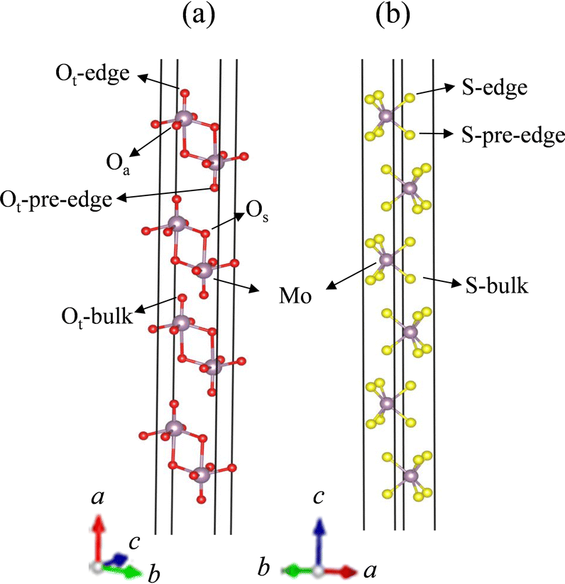 | ||
| Fig. 1 The unit cells of (a) 4L α-MoO3 and (b) 6L 2H-MoS2. The purple, red and yellow balls in the geometrical models represent the Mo, O and S atoms, respectively. | ||
The geometry optimizations of all pristine and substituted MoO3 and MoS2 layered structures were performed by using the ab initio CRYSTAL17 code34 within periodic boundary conditions and localized Gaussian-type function basis sets (BSs). The convergence criterion for the geometry optimization was fixed at 10−10 Ha per unit cell. The following BSs were used: Mo_SC_HAYWSC-311(d31)G_cora_199735 (for Mo atoms), S_86-311G*_lichanot_199336 (for S atoms) and O_8-411d11G_valenzano_200637 (for O atoms). For the exchange-correlation potential, the PBE functional38 has been adopted and the van der Waals contributions were described by using the semi-empirical Grimme D3 approach39 with optimized scaling factors.32 The tolerances for the evaluation of Coulomb and exchange series were set to 8 × 8 × 8 × 8 × 16.34 Since ordinary DFT within the PBE/GGA functional underestimates the electronic band gap, all the electronic properties were computed via single-point calculations by using the range separated hybrid Heyd–Scuseria–Ernzerhof (HSE06) exchange correlation functional40,41 on the PBE optimized geometries using CRYSTAL17. The wave functions were converged with a SCF energy convergence criterion of 10−10 Ha per unit-cell and the reciprocal space for the unit-cell of pristine FL MoS2 and FL MoO3 systems is sampled according to a sublattice with a 12 × 12 k-point mesh. The k-point mesh sampling was progressively reduced as the size of the SL and FL unit cells increases for the doped materials (Tables S2 and S3, ESI†).
Due to the large number of structures and their large number of atoms, it was not possible to make systematic phonon analyses. However, to check for the relevance of the various FL MoO3−xSx and MoS2−xOx systems simulated, their relative thermodynamic stability was analyzed through three types of descriptors: (i) binding energy (Tables S1 and S2, ESI†), (ii) reaction energy and (iii) thermodynamic phase diagram. The equations for the reaction energy of S/O exchanges in FL MoO3−xSx and MoS2−xOx with H2S/H2O and for the grand potential approach used for the determination of thermodynamic phase diagrams of FL MoO3−xSx and MoS2−xOx as a function of T and  are reported in the ESI,† 2.2. The approach follows the original one proposed in ref. 42 and applied earlier for the sulfo-reduction of MoS2 slabs43 and more recently for the MoO3−xSx and MoS2−xOx bulk materials.32
2.2. Optical properties
The absorption coefficient is evaluated from the dielectric matrix εαβ(ω) using the Kramers–Kronig transformation.44 The optical properties were evaluated within the HSE06 functional by using the Vienna ab initio simulation package (VASP)45–47 with a kinetic energy cut-off of 500 eV for the plane wave basis set and the project augmented wave (PAW)48 pseudopotentials for Mo, O and S atoms. The previously PBE optimized structures with CRYSTAL were used for the optical calculations with a 20 Å vacuum distance in order to avoid interactions with images of the systems along the thickness of the nanosheets. We set a denser k-point mesh size of 24 × 24 × 1 Γ-centered Monkhorst–Pack49 to evaluate optical properties. For more details about the calculations of optical properties, see our previous studies.32,332.3. High frequency dielectric constant profile ε∞(z)
In order to extract the optical (high frequency) dielectric constant profile along the out-of-plane direction (z-axis) in 2D systems, we followed a DFT scheme based on polarization variations in response to a finite electric field.50–52 This method was performed51–55 to calculate the dielectric constant profile using the local orbital SIESTA56 code within the simple LDA57 or GGA38 functionals so far. For the first time, in our previous work, we performed this method using the CRYSTAL results of the electronic density within the range separated the hybrid functional HSE06.41 As detailed in ref. 50 and 52, the calculation of the microscopic dielectric profile requires applying an external electric field, we analyzed the band gap evolution of each 2D layered MoO3 and MoS2 structures as a function of this external electric field applied perpendicularly to the layer planes (Fig. S1, ESI†). Then, we checked that the induced dipole in 2D MoO3 and MoS2 layered structures scales linearly with the number of layers for very small external electric field, Eext = 0.025 eV Å−1, as shown in Fig. S2 (ESI†). Hence, all dielectric constant profiles (ε∞) are calculated for Eext = 0.025 eV Å−1. For more details about the calculations of the dielectric constant profile, the reader should refer to our previous work.333. Results
3.1 Pristine structures of few-layer MoO3 and MoS2
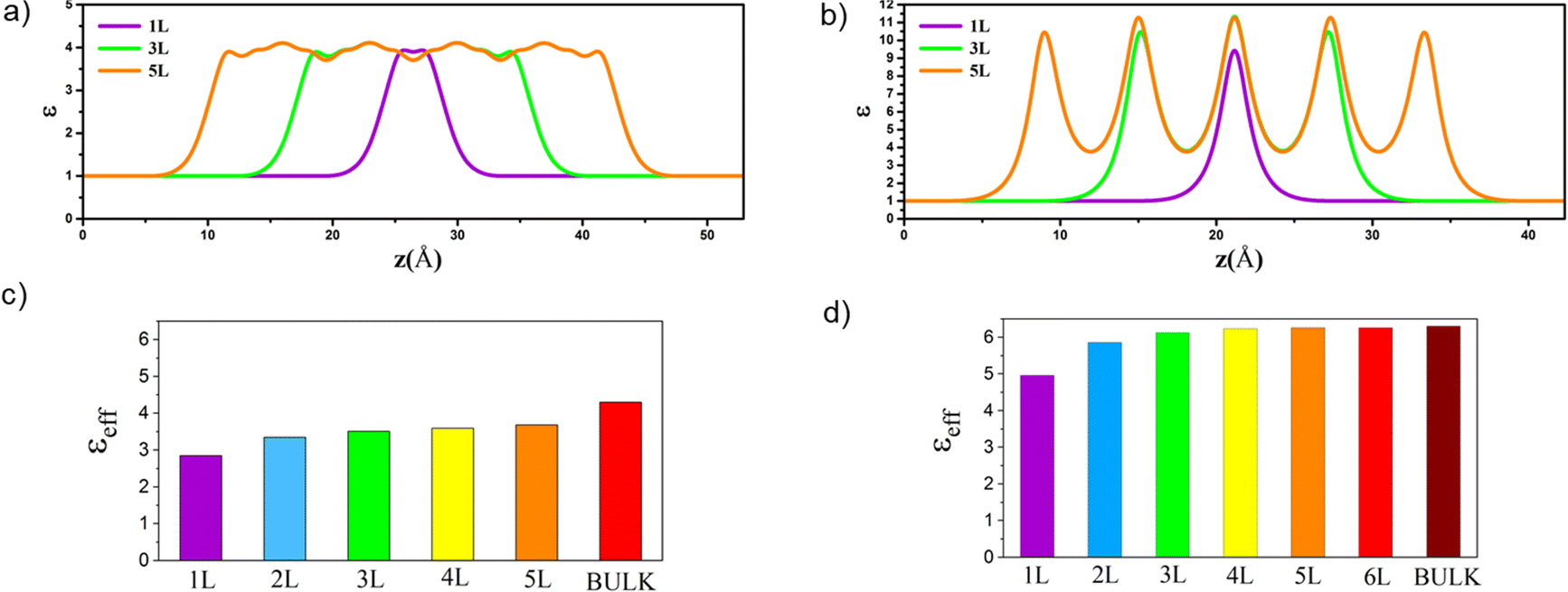 | ||
| Fig. 2 Dielectric constant profiles (ε) along out-of-plane for 1L, 3L and 5L MoO3 (a) and 1L, 3L and 5L MoS2 (b). The effective dielectric constant along out-of-plane for 1L–5L and bulk MoO3 (c) and 1L–6L and bulk MoS2 (d). The effective dielectric constants for 3D bulk phases are also included according to our previous work.32 | ||
In addition, the calculated optical absorption coefficients confirm the highly anisotropic optical properties of both pristine MoO3 and MoS2 systems considering in-plane and out-of-plane absorption coefficients (Fig. S3, ESI†). For both layered structures, the in-plane absorption coefficient is greater than that of the out-of-plane one. The absorption spectra increase in the UV-vis range, notably for the out-of-plane direction, by increasing the number of layers, whereas the electronic band gaps for layered MoO3 systems remain in the same range.33 These results also show that by increasing the number of layers the absorption coefficient of the MoS2 nanosheets increases more significantly than that of MoO3 and is enhanced in the UV-vis range, while the band gaps increase continuously with the number of layers.33 Furthermore, high absorption coefficients were achieved for all MoO3 and MoS2 FLs, in particular along the in-plane direction, which is higher than the typical optical absorption for direct band gap semiconductors in the UV-vis range.32,62
3.2 S-doped 4L MoO3 and O doped 6L MoS2
Fig. 3 and Fig. S7a (ESI†) illustrate the thermodynamic phase diagrams of substituted 4L MoO3−xSx and 6L MoS2−xOx systems with respect to the pristine structures considering the H2S/H2O reservoir by using the Grand potential approach. It is conspicuous that the sulfidation of pristine 4L MoO3 nanosheets requires a value of  as high as −0.36 eV. For
  in the range between −0.36 eV and −0.19 eV, the structure with 4.16% S is thermodynamically favored and for
  it is higher than −0.19 eV, the 4L MoSxO3−x system with 33% S is the most stable. These results are different from those obtained on bulk materials, where the
  value required for sulfide MoO3 was significantly greater (∼0.1 eV). As shown in Fig. 3, this trend is mainly induced by the easier sulfidation of Ot located at edges, exhibiting lower Grand potential values than the ones corresponding to bulk substitution. Generally, the O/S exchange process is exergonic when Ot located at edges are involved, whereas it was endergonic for the bulk materials.32 This shows that FL MoO3 materials are much easier to sulfide than bulk materials. The most stable compositions correspond to 4.16% S and 33% S although one cannot exclude the 8.33%S and 16.66% S ones according to the methodology accuracy. All these systems will be considered for the opto-electronic analyses. From an experimental point of view, it has been shown that it is possible to reach high S-doping concentrations which would require to substitute not only top-oxo but also bridging-oxo species leading to more complex reconstructed Mo oxy-sulfides.64,65 Hence, it seems relevant to propose the S-dopant concentration as high as 33%. This doping process is all the easier as the material will expose many edges and near edge sites exchangeable with S.
 | ||
| Fig. 3 Thermodynamic phase stability of the S-substituted 4L MoO3 considering the H2S/H2O reservoir. The dashed and dotted lines denote the results for impurity-substituted only in the edge and the bulk of layered systems, respectively. | ||
Regarding the 6L MoS2 material, the free energies for oxidation (Fig. S6a, ESI†) are all endergonic. Hence, oxidation starts for  higher than ∼0.75 eV, and the oxidized structure with the highest O concentration (75%) should be the least unfavored. The
  value obtained for the bulk MoS2 material was at ∼0.75 eV.32 Fig. S6a (ESI†) shows that edge doped systems are nearly superimposed to the bulk doped ones meaning that almost no energy gain is obtained. Hence, the impact of edge oxidation is negligible for this system: the intrinsic unfavorable S/O exchange is due to the poor lability of tri-coordinated S-atoms present in MoS2. Although the chemical systems are different, this trend seems to be qualitatively comparable with previous experimental results having shown that only a very low concentration of SnS2 can be oxidized into SnO2.66
As a consequence, this analysis reveals that the sulfidation of 4L MoO3 is thermodynamically more favorable than the oxidation of 6L MoS2 when we consider H2S/H2O as reactants or products. Moreover, the sulfidation of 4L MoO3 is enhanced at edges which may also impact the electronic properties investigated in the following section.
 | ||
| Fig. 4 (a and b) Computed electronic band gap values (in eV) and (c and d) absorption coefficients (α, in cm−1) along in-plane and out-of-plane of the most stable S-substituted 4L MoO3 (a and c) and O-substituted 6L MoS2 (b and d) for different S- and O-concentrations. The hatching patterns in the bar graphs and dashed lines in the absorption spectra are related to those structures in which impurities substituted at the edge. | ||
Moreover, as it is illustrated by the various configurations simulated for MoS0.25O2.75 (xs = 8.33%) and MoS0.5O2.5 (xs = 16.7%), the interaction between the S atoms and O atoms at the nearest layers leads to a decrease in the electronic band gap (Fig. S7, ESI†). A relevant example for which the band gap evolves in three different configurations is illustrated in Fig. 5 for MoS0.5O2.5 (xs = 16.7%). The band gap is maximized (1.85 eV) when S-atoms are not located in close vicinity of the O-atoms of the nearest layer (configuration of Fig. 5c), whereas it is significantly reduced when 2 S atoms are facing 2 O atoms located either at the pre-edge (configuration of Fig. 5a) or at the inner layer (Fig. 5b). The corresponding PDOS reported in Fig. 5 highlights how the occupied 3p-states of S atoms (either in the bulk or at the pre-edge) located at the top of the VB are pushing down the unoccupied 2p-states of O atoms (either at the pre-edge or in the bulk, respectively) at the bottom of the CB upon interaction. This induces a downward shift of the CB band (as illustrated later) and a closure of the band gap in the extreme case as shown in Fig. 5a. The configuration of Fig. 5a where the two central layers are sulfided and sandwiched between two MoO3 layers is qualitatively comparable to previous calculations on the SL MoO3/MoS2 heterojunction which has a metallic character because of the proximity of S and O at the interface of two layers,33 while for S-doped MoO3 at the interface of MoO3/MoS2 with concentrations equal to or greater than 5.6%, a metal–semiconductor transition occurs.33 Lastly, it is interesting to notice that all S-doped 4L MoO3 systems exhibit a significant decrease of the band gap (by at least 0.74 eV) with respect to their homologous doped SL MoO3 system, while the band gap of the non-doped MoO3 system does not depend on the number of layers.33
 | ||
| Fig. 5 Optimized structures, electronic band structures and PDOS of 4L MoS0.5O2.5 (xs = 16.66%) for 3 different S substitution positions calculated by using HSE06: (a) inside the bulk only, (b) at edge and pre-edge, (c) at edge and in the bulk. The Fermi level is set to zero. The corresponding structures, band structures and PDOS for these systems are also reported in Fig. S3 and S5 (ESI†) configurations h, i, and j, respectively. | ||
In contrast, the indirect band gap feature in 6L MoS2 also remains unchanged within substituting sulfur atoms by oxygen atoms. The band gap value of 6L MoOxS2−x is first decreased by minimum O doping and then begins to enhance by increasing the O concentration of up to 75% (Fig. 4 and Table S2, ESI†). However, from a general point of view, either bulk or edge sites used for the substitution of O atoms in 6L MoS2−xOx produce very similar electronic properties as illustrated by PDOS analysis (Fig. S8, ESI†). This trend is similar to the analysis already made on bulk MoS2−xOx.32 Due to the Mott insulator character of MoS2, the nature of the CB/VB bands are dominated by Mo 4d states induced by a1g–eg splitting in the trigonal prismatic Mo environment. The 2p states of the O dopants are thus located at energy levels which do not impact strongly the evolution of the band gaps and the CB/VB of the pristine 6L MoS2 system.
The optical property analysis (Fig. 4) of these FL materials confirms that by increasing the S concentration on 4L MoO3 the in-plane and out-of-plane absorption coefficients are enhanced in the UV-vis range while it is reduced monotonically in 6L MoS2 by increasing the O concentration. Moreover, the S-doped 4L MoO3 materials clearly reveal a stronger absorption in the visible range than the previously studied S-doped SL MoO3 materials.33 The different impurity sites (bulk and edge) for the low concentration level produce nearly the same absorption coefficient along the in-plane direction in both materials while edge substitutions lead to enhanced adsorption spectra along the out-of-plane direction. All doped FL structures have an indirect band gap feature, and their absorption coefficient is thus notably low for the photon energy close to the bandgap. However, for wavelengths below 500 nm, direct transitions are possible allowing to reach high absorption coefficients (∼105 cm−1) and comparable to those of organic perovskite solar cells.67,68 These results indicate that these systems possess significant light-harvesting capabilities for the solar spectrum in the UV-visible range of light.32,62
 | ||
| Fig. 6 Calculated conduction and valence band-edge positions of (a) S-substituted 4L MoO3 (only for the most stable cases) and (b) O-substituted 6L MoS2 with respect to the vacuum level and the standard hydrogen electrode. The band edge position for SL MoS2 is also presented in (a). The lower edge of the conduction band (orange color) and the upper edge of the valence band (blue color) are presented along with the band gap in electron volts. The dashed green lines indicate the water stability limits for the hydrogen and oxygen evolution reactions. The absolute potential of the standard hydrogen electrode was taken as 4.44 eV at a pH = 0. | ||
Hence, to generate a good material for water oxidation and O2 evolution, either the edges must be covered by S-atoms or all top oxo-species (at edges and in the bulk) must be replaced by S. In contrast, isolated top-oxo species remaining inside the partially S-doped MoO3 bulk are detrimental. The CB levels of the S-doped MoO3 4L systems with 8.33%S (edge), 16.66% (edge + bulk) and 33% (edge + bulk) are predicted to be at the same level as the water photo-oxidation potential for O2 evolution only, which is not enough to overcome the expected overpotential. Hence, to tackle the challenge of water photolysis, the S-doped MoO3 FL systems cannot be used alone but it must be involved within a heterostructure involving either SL or ML MoS2 as analyzed in the following.
As a result of the previous PDOS analysis, the location of O substituted in 6L MoS2 does not produce any significant change in the VB edge positions (Fig. 6b). The CB edge positions for these O-doped systems slightly shift to lower energies (even lower to the required level for H2 evolution). Hence they possess suitable band edge positions only for water oxidation and O2 evolution.
In our recent paper,33 we proposed strategies to tune the transitions from type III to type II band alignment of materials made of the 2D SL MoO3−xSx/SL MoS2 heterostructure. Here, since the CB edge positions of FL MoO3−xSx (with S at edges) shift to higher energy levels, we can extend our previous proposals by considering heterostructures made of 4L MoSxO3−x/SL MoS2 and 4L MoSxO3−x/FL MoS2 to optimize at best the composite material as a function of stacking. One should underline that one strong advantage of the 4L MoSxO3−x material with respect to the previously studied SL MoSxO3−x is its stronger absorption coefficient in the visible range as previously shown in Fig. 4.
By analyzing first the VB and CB edge levels of 4L MoSxO3−x and SL MoS2 layers (Fig. 6a), we identify potential 2D heterojunctions made of 4L MoSxO3−x and SL MoS2 layers that would lead to the type II band alignment with targeted concentrations and locations of S into MoO3 layers: 8.33% (at the edge of layers), 16.66% and 33%. For 16.66%S, the control of the precise positions of S atoms located inside the bulk should make this system difficult to handle experimentally. These proposed type II heterostructures could thus be good candidates for photocatalytic applications since they may potentially generate a direct Z-scheme due to the proximity of the CB of 4L MoSxO3−x to the VB of SL MoS2, although the band gaps of the heterostructures with 8.33%, 16.66% and 33% are larger (∼0.83 eV) than those in the case of the SL MoSxO3−x/MoS2 heterojunction (0.4 eV).33 For all other S concentrations, these interfaces are type III heterojunction resulting from the lower CB positions of 4L MoSxO3−x layers rather than the VB position of SL MoS2.
Finally, the CB positions in 4L MoSxO3−x doped with 8.33%S (at the edge) and 16.66%S are ∼0.6 and ∼0.7 eV, respectively, higher than those of the SL MoSxO3−x doped with a similar S concentration.33 For 4L MoSxO3−x doped with 33%S, the CB position is quite high too, similar to the SL case. This implies that it is potentially more efficient to combine these 3 structures with the non-doped MoS2 SL materials to build a type II heterojunction or a Z-scheme system. Indeed, the CB positions of these 4L MoSxO3−x are slightly above the VB of the non-doped MoS2 SL materials leading to a small band gap heterostructure which may be in favor of a charge transfer from MoS2 to MoSxO3−x before illumination as analyzed in ref. 33 for the SL heterostructure. In addition, the 4L MoSxO3−x structures doped with 8.33%S (at the edge), 16.66%S and 33%S are compatible with the non-doped MoS2 FL structure.
As a general consequence, to optimize the band gap and charge transfer, the best heterojunctions should be either the SL MoSxO3−x/SL MoS2 heterostructure with 8.3%S doping in MoSxO3−x as previously invoked33 or alternatively FL MoSxO3−x with edge S-doping of 8.3, 16.7 or 33% and SL or FL MoS2 as proposed in the present work. Since the 4L MoSxO3−x doped with 33%S is thermodynamically stable (Fig. 3), this structure may be a good candidate for building a heterojunction with a FL MoS2 material (such as the 6L one studied here). These optimal heterostructures lead to type II heterojunctions as proposed for other systems.69,70 In this case, the CB position of FL MoSxO3−x is located just above the VB of FL MoS2 which may also provide an optimal situation for a Z-scheme behavior where the electrons photogenerated at the CB of FL MoSxO3−x recombine with the hole generated on the VB of FL or SL MoS2. At the same time, the electrons generated at the CB of FL or SL MoS2 will reduce the proton into H2, while the hole of the VB of FL MoSxO3−x will oxidize the water into O2.
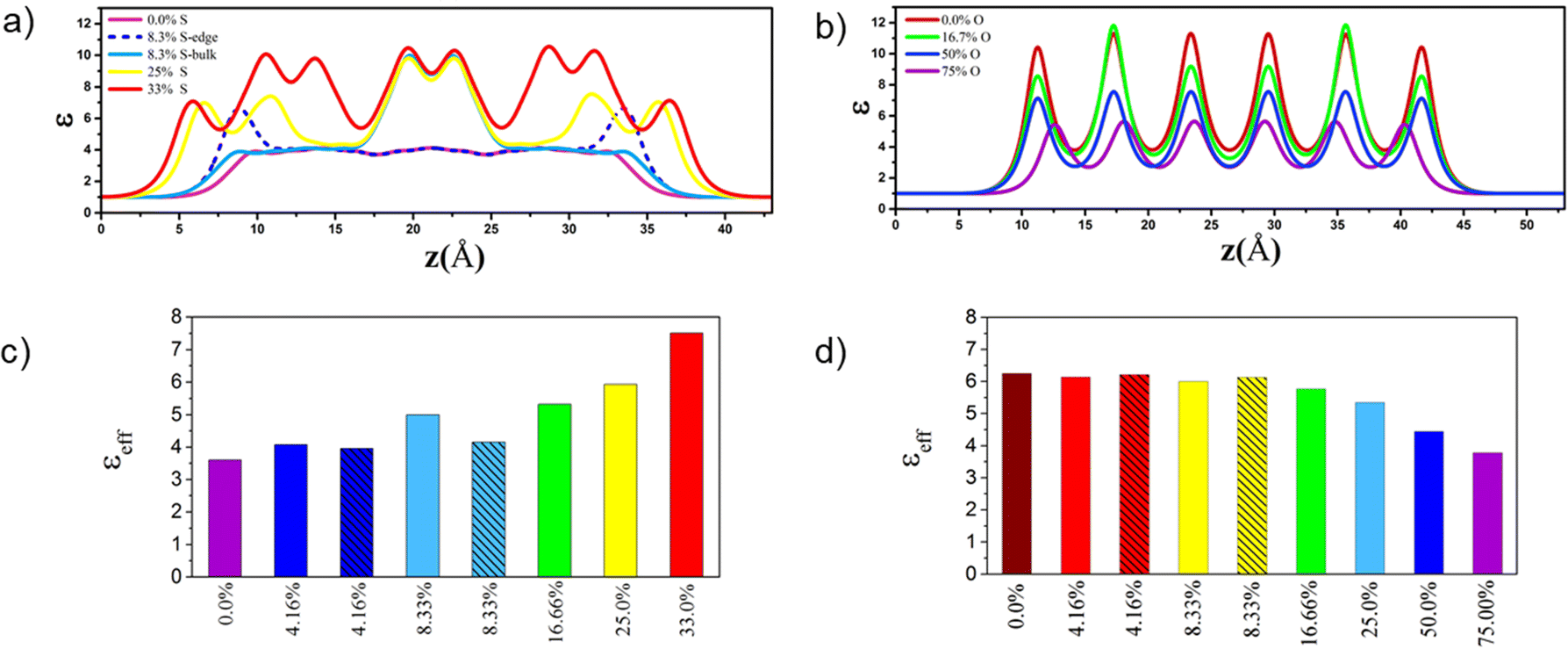 | ||
| Fig. 7 Dielectric constant profiles (ε) along out-of-plane of S-substituted 4L MoO3 (a) and O-substituted 6L MoS2 (b) for different S- and O-concentrations. The effective dielectric constants along out-of-plane of S-substituted 4L MoO3 (c) and O-substituted 6L MoS2 (d) for different S- and O-concentrations. The hatching patterns in the bar graphs and dashed lines in the dielectric profile are related to those structures in which impurities substituted at the edge only. | ||
4. Conclusion
We used DFT calculations within the HSE06 functional to characterize the opto-electronic properties and high frequency dielectric constant profiles of sulfur doped MoO3 and oxygen doped MoS2 FL structures. The thermodynamic phase diagram for various concentrations of S doped 4L MoO3 structures in the H2S/H2O environment revealed that the structures with 4.16%S at the edge, 8.33%S at the edge, and 16.66 and 33%S concentrations can be stabilized with a reasonable ratio. Moreover, we showed that the MoO3−xSx structures with S-impurities at the edge of nanolayers are more stable than those having impurities in the bulk. This specific edge location is beneficial for the opto-electronic properties (band gaps and CB/VP levels) and the absorption spectrum. The sulfur doping of 4L MoO3 induces a decrease of the electronic band gap (from 2.92 eV to 1.44 eV). The stronger band gap reductions are obtained when S-atoms are located inside the bulk and interact with O-atoms located in neighboring layers, while the CB and VB positions are shifted to lower potential values in the case of the edge location of S-atoms. This doping induces an increase of the dielectric constant profile and absorption coefficient in the UV-vis range, which is significantly enhanced in the visible range when compared with the previous S-doped SL MoO3 material.33
In contrast, it is less favorable to substitute S atoms by O atoms in 6L MoS2 under the same conditions. Moreover, substituting sulfur atoms by oxygen atoms on 6L MoS2 for the 4.16% O concentration abruptly decreases the electronic band gap from 1.73 eV in the pristine material to around 1.2 eV. Then the electronic band gap of 6L MoS2−xOx begins to enhance with the increasing O concentration which induces a decrease of the dielectric constant profile and absorption coefficient in the UV-vis range. Hence, O-doping of MoS2 either as the SL, FL or bulk does not provide significant improvements of the properties of the MoS2 material.
As a consequence, to reach the targeted properties for water photocatalytic dissociation into O2 and H2, we proposed relevant heterostructures leading to type II heterojunctions which may contain either FL or SL components. In particular, we identified the stable 4L MoSxO3−x doped with 8.33%S at the edge and 16.66%S (edge + bulk) and 33%S in combination with the FL or SL MoS2 as potential good candidates for the Z-scheme formalism. Moreover since the 4L MoSxO3−x doped with 33% S provides the largest effective dielectric constant, we suggest that this system should be particularly appealing for screening the photogenerated charges. Hence, the present work provides additional relevant heterostructures supplementing our previous work devoted mainly to SL MoSxO3−x/SL MoS2 systems.33 This finding is of practical interest for experimental implementation because it allows more flexibility for the number of layers to be targeted at the synthesis steps without being limited to the SL MoSxO3−x/MoS2 heterojunction. It also highlights the great versatility of heterostructures made of a variable number of layers of MoSxO3−x and MoS2 usable in photocatalytic applications.
Conflicts of interest
There are no conflicts to declare.Acknowledgements
This work is part of the “RatiOnAl Design for CATalysis” (ROAD4CAT) industrial chair, project IDEXLYON funded by the French National Research Agency (ANR-16-IDEX-0005) and the Commissariat-General for Investment (CGI) within the framework of Investissements d’Avenir program (“Investment for the future”). The authors thank the SYSPROD project and AXELERA Pôle de Compétitivité for financial support (PSMN Data Center). This work was granted access to the HPC resources of CINES, IDRIS and TGCC under the allocation 2018-080609 made by GENCI.References
- K. S. Novoselov, A. K. Geim, S. V. Morozov, D. Jiang, Y. Zhang, S. V. Dubonos, I. V. Grigorieva and A. A. Firsov, Electric Field Effect in Atomically Thin Carbon Films, Science, 2004, 306, 666 CrossRef CAS PubMed.
- Y. Kubota, K. Watanabe, O. Tsuda and T. Taniguchi, Deep Ultraviolet Light-Emitting Hexagonal Boron Nitride Synthesized at Atmospheric Pressure, Science, 2007, 317, 932 CrossRef CAS PubMed.
- P. Vogt, P. de Padova, C. Quaresima, J. Avila, E. Frantzeskakis, M. C. Asensio, A. Resta, B. Ealet and G. Le Lay, Silicene: compelling experimental evidence for graphene like two-dimensional silicon, Phys. Rev. Lett., 2012, 108, 155501 CrossRef PubMed.
- S. Balendhran, S. Walia, H. Nili, S. Sriram and M. Bhaskaran, Elemental Analogues of Graphene: Silicene, Germanene, Stanene, and Phosphorene, Small, 2015, 11, 640–652 CrossRef CAS PubMed.
- J. Miao, C. Chen, L. Meng and Y. S. Lin, Self-Assembled Monolayer of Metal Oxide Nanosheet and Structure and Gas-Sensing Property Relationship, ACS Sens., 2019, 4, 1279–1290 CrossRef CAS PubMed.
- T. Yang, T. T. Song, M. Callsen, J. Zhou, J. W. Chai, Y. P. Feng, S. J. Wang and M. Yang, Atomically Thin 2D Transition Metal Oxides: Structural Reconstruction, Interaction with Substrates, and Potential Applications, Adv. Mater. Interfaces, 2019, 6, 1801160 CrossRef.
- K. F. Mak, C. Lee, J. Hone, J. Shan and T. F. Heinz, Atomically Thin MoS2: A New Direct-Gap Semiconductor, Phys. Rev. Lett., 2010, 105, 136805 CrossRef PubMed.
- M. Naguib, V. N. Mochalin, M. W. Barsoum and Y. Gogotsi, 25th Anniversary Article: MXenes: A New Family of Two-Dimensional Materials, Adv. Mater., 2014, 26, 992–1005 CrossRef CAS PubMed.
- H. Liu, A. T. Neal, Z. Zhu, Z. Luo, X. Xu, D. Tománek and P. D. Ye, Phosphorene: An Unexplored 2D Semiconductor with a High Hole Mobility, ACS Nano, 2014, 8, 4033–4041 CrossRef CAS PubMed.
- M. M. Furchi, A. Pospischil, F. Libisch, J. Burgdörfer and T. Mueller, Photovoltaic Effect in an Electrically Tunable van der Waals Heterojunction, Nano Lett., 2014, 14, 4785–4791 CrossRef CAS PubMed.
- K. Xu, Y. Wang, Y. Zhao and Y. Chai, Modulation doping of transition metal dichalcogenide/oxide heterostructures, J. Mater. Chem. C, 2017, 5, 376–381 RSC.
- S. KC, R. C. Longo, R. Addou, R. M. Wallace and K. Cho, Electronic properties of MoS2/MoOx interfaces: Implications in Tunnel Field Effect Transistors and Hole Contacts, Sci. Rep., 2016, 6, 33562 CrossRef PubMed.
- Z. Gao, Z. Zhou and D. Tománek, Degenerately Doped Transition Metal Dichalcogenides as Ohmic Homojunction Contacts to Transition Metal Dichalcogenide Semiconductors, ACS Nano, 2019, 13, 5103–5111 CrossRef CAS PubMed.
- B. Wang, H. Luo, X. Wang, E. Wang, Y. Sun, Y.-C. Tsai, J. Dong, P. Liu, H. Li, Y. Xu, S. Tongay, K. Jiang, S. Fan and K. Liu, Direct laser patterning of two-dimensional lateral transition metal disulfide-oxide-disulfide heterostructures for ultrasensitive sensors, Nano Res., 2020, 13, 2035–2043 CrossRef CAS.
- J. Azadmanjiri, P. Kumar, V. K. Srivastava and Z. Sofer, Surface Functionalization of 2D Transition Metal Oxides and Dichalcogenides via Covalent and Non-covalent Bonding for Sustainable Energy and Biomedical Applications, ACS Appl. Nano Mater., 2020, 3, 3116–3143 CrossRef CAS.
- P. Carcia and E. McCarron, Synthesis and properties of thin film polymorphs of molybdenum trioxide, Thin Solid Films, 1987, 155, 53–63 CrossRef CAS.
- M. Kröger, S. Hamwi, J. Meyer, T. Riedl, W. Kowalsky and A. Kahn, Role of the deep-lying electronic states of MoO3 in the enhancement of hole-injection in organic thin films, Appl. Phys. Lett., 2009, 95, 123301 CrossRef.
- K. K. Kam and B. A. Parkinson, Detailed photocurrent spectroscopy of the semiconducting group VIB transition metal dichalcogenides, J. Phys. Chem., 1982, 86, 463–467 CrossRef CAS.
- Y.-J. Yuan, Z.-J. Ye, H.-W. Lu, B. Hu, Y.-H. Li, D.-Q. Chen, J.-S. Zhong, Z.-T. Yu and Z.-G. Zou, Constructing Anatase TiO2 Nanosheets with Exposed (001) Facets/Layered MoS2 Two-Dimensional Nanojunctions for Enhanced Solar Hydrogen Generation, ACS Catal., 2016, 6, 532–541 CrossRef CAS.
- Y. Li, Y.-L. Li, B. Sa and R. Ahuja, Review of two-dimensional materials for photocatalytic water splitting from a theoretical perspective, Catal. Sci. Technol., 2017, 7, 545–559 RSC.
- C. Maheu, E. Puzenat, C. Geantet, L. Cardenas and P. Afanasiev, Titania - Supported transition metals sulfides as photocatalysts for hydrogen production from propan-2-ol and methanol, Int. J. Hydrogen Energy, 2019, 44, 18038–18049 CrossRef.
- B. Zheng, Z. Wang, Y. Chen, W. Zhang and X. Li, Centimeter-sized 2D α-MoO3 single crystal: growth, Raman anisotropy, and optoelectronic properties, 2D Mater., 2018, 5, 45011 CrossRef CAS.
- F. Rahman, T. Ahmed, S. Walia, E. Mayes, S. Sriram, M. Bhaskaran and S. Balendhran, Two-dimensional MoO3 via a top-down chemical thinning route, 2D Mater., 2017, 4, 35008 CrossRef.
- J. Sun, X. Li, W. Guo, M. Zhao, X. Fan, Y. Dong, C. Xu, J. Deng and Y. Fu, Synthesis Methods of Two-Dimensional MoS2: A Brief Review, Crystals, 2017, 7, 198 CrossRef.
- Y.-H. Lee, X.-Q. Zhang, W. Zhang, M.-T. Chang, C.-T. Lin, K.-D. Chang, Y.-C. Yu, J. T.-W. Wang, C.-S. Chang, L.-J. Li and T.-W. Lin, Synthesis of Large-Area MoS2 Atomic Layers with Chemical Vapor Deposition, Adv. Mater., 2012, 24, 2320–2325 CrossRef CAS PubMed.
- S. L. Howell, D. Jariwala, C.-C. Wu, K.-S. Chen, V. K. Sangwan, J. Kang, T. J. Marks, M. C. Hersam and L. J. Lauhon, Investigation of Band-Offsets at Monolayer–Multilayer MoS2 Junctions by Scanning Photocurrent Microscopy, Nano Lett., 2015, 15, 2278–2284 CrossRef CAS PubMed.
- R. Favre, P. Raybaud and T. Le Bahers, Electronic structures of the MoS2/TiO2 (anatase) heterojunction: influence of physical and chemical modifications at the 2D- or 1D-interfaces, Phys. Chem. Chem. Phys., 2022, 24, 2646–2655 RSC.
- F. Li and Z. Chen, Tuning electronic and magnetic properties of MoO3 sheets by cutting, hydrogenation, and external strain: a computational investigation, Nanoscale, 2013, 5, 5321–5333 RSC.
- T. Su, Q. Shao, Z. Qin, Z. Guo and Z. Wu, Role of Interfaces in Two-Dimensional Photocatalyst for Water Splitting, ACS Catal., 2018, 8, 2253–2276 CrossRef CAS.
- T. Le Bahers, M. Rérat and P. Sautet, Semiconductors Used in Photovoltaic and Photocatalytic Devices: Assessing Fundamental Properties from DFT, J. Phys. Chem. C, 2014, 118, 5997–6008 CrossRef.
- X. Li, C. Garlisi, Q. Guan, S. Anwer, K. Al-Ali, G. Palmisano and L. Zheng, A review of material aspects in developing direct Z-scheme photocatalysts, Mater. Today, 2021, 47, 75–107 CrossRef CAS.
- M. Shahrokhi, P. Raybaud and T. Le Bahers, On the understanding of the optoelectronic properties of S-doped MoO3 and O-doped MoS2 bulk systems: a DFT perspective, J. Mater. Chem. C, 2020, 8, 9064–9074 RSC.
- M. Shahrokhi, P. Raybaud and T. Le Bahers, 2D MoO3−xSx/MoS2 van der Waals Assembly: A Tunable Heterojunction with Attractive Properties for Photocatalysis, ACS Appl. Mater. Interfaces, 2021, 13, 36465–36474 CrossRef CAS PubMed.
- R. Dovesi, A. Erba, R. Orlando, C. M. Zicovich-Wilson, B. Civalleri, L. Maschio, M. Rérat, S. Casassa, J. Baima, S. Salustro and B. Kirtman, Quantum-mechanical condensed matter simulations with CRYSTAL, Wiley Interdiscip. Rev.: Comput. Mol. Sci., 2018, 8, e1360 Search PubMed.
- F. Corà, A. Patel, N. M. Harrison, C. Roetti and C. R. A. Catlow, Anab initio Hartree–Fock study of α- MoO3, J. Mater. Chem., 1997, 7, 959–967 RSC.
- A. Lichanot, E. Aprà and R. Dovesi, Quantum Mechnical Hartree-Fock Study of the Elastic Properties of Li2S and Na2S, Phys. Status Solidi B, 1993, 177, 157–163 CrossRef CAS.
- L. Valenzano, F. J. Torres, K. Doll, F. Pascale, C. M. Zicovich-Wilson and R. Dovesi, Ab Initio Study of the Vibrational Spectrum and Related Properties of Crystalline Compounds; the Case of CaCO3 Calcite, Z. Phys. Chem., 2006, 220, 893–912 CrossRef CAS.
- J. P. Perdew, K. Burke and M. Ernzerhof, Generalized Gradient Approximation Made Simple, Phys. Rev. Lett., 1996, 77, 3865–3868 CrossRef CAS PubMed.
- S. Grimme, J. Antony, S. Ehrlich and H. Krieg, A consistent and accurate ab initio parametrization of density functional dispersion correction (DFT-D) for the 94 elements H-Pu, J. Chem. Phys., 2010, 132, 154104 CrossRef PubMed.
- J. Heyd, G. E. Scuseria and M. Ernzerhof, Hybrid functionals based on a screened Coulomb potential, J. Chem. Phys., 2003, 118, 8207–8215 CrossRef CAS.
- J. Heyd, G. E. Scuseria and M. Ernzerhof, Erratum: “Hybrid functionals based on a screened Coulomb potential” [J. Chem. Phys. 118, 8207 (2003)], J. Chem. Phys., 2006, 124, 219906 CrossRef.
- M. Scheffler and J. Dabrowski, Parameter-free calculations of total energies, interatomic forces and vibrational entropies of defects in semiconductors, Philos. Mag. A, 1988, 58, 107–121 CrossRef CAS.
- P. Raybaud, J. Hafner, G. Kresse, S. Kasztelan and H. Toulhoat, Ab Initio Study of the H2–H2S/MoS2 Gas–Solid Interface: The Nature of the Catalytically Active Sites, J. Catal., 2000, 189, 129–146 CrossRef CAS.
- F. Wooten, Optical Properties of Solids, Elsevier Science, Burlington, 2013 Search PubMed.
- G. Kresse and J. Furthmüller, Efficient iterative schemes for ab initio total-energy calculations using a plane-wave basis set, Phys. Rev. B: Condens. Matter Mater. Phys., 1996, 54, 11169–11186 CrossRef CAS PubMed.
- G. Kresse and J. Furthmüller, Efficiency of ab-initio total energy calculations for metals and semiconductors using a plane-wave basis set, Comput. Mater. Sci., 1996, 6, 15–50 CrossRef CAS.
- G. Kresse and J. Hafner, Ab initio molecular dynamics for liquid metals, Phys. Rev. B: Condens. Matter Mater. Phys., 1993, 47, 558–561 CrossRef CAS PubMed.
- P. E. Blöchl, Projector augmented-wave method, Phys. Rev. B: Condens. Matter Mater. Phys., 1994, 50, 17953–17979 CrossRef PubMed.
- H. J. Monkhorst and J. D. Pack, Special points for Brillouin-zone integrations, Phys. Rev. B: Solid State, 1976, 13, 5188–5192 CrossRef.
- F. Giustino, P. Umari and A. Pasquarello, Dielectric Discontinuity at Interfaces in the Atomic-Scale Limit: Permittivity of Ultrathin Oxide Films on Silicon, Phys. Rev. Lett., 2003, 91, 267601 CrossRef PubMed.
- D. Sapori, M. Kepenekian, L. Pedesseau, C. Katan and J. Even, Quantum confinement and dielectric profiles of colloidal nanoplatelets of halide inorganic and hybrid organic–inorganic perovskites, Nanoscale, 2016, 8, 6369–6378 RSC.
- J. Even, L. Pedesseau and M. Kepenekian, Electronic surface states and dielectric self-energy profiles in colloidal nanoscale platelets of CdSe, Phys. Chem. Chem. Phys., 2014, 16, 25182–25190 RSC.
- R. Ramprasad and N. Shi, Dielectric properties of nanoscale HfO2 slabs, Phys. Rev. B: Condens. Matter Mater. Phys., 2005, 72, 52107 CrossRef.
- N. Shi and R. Ramprasad, Dielectric properties of ultrathin SiO2 slabs, Appl. Phys. Lett., 2005, 87, 262102 CrossRef.
- N. Shi and R. Ramprasad, Atomic-scale dielectric permittivity profiles in slabs and multilayers, Phys. Rev. B: Condens. Matter Mater. Phys., 2006, 74, 45318 CrossRef.
- J. M. Soler, E. Artacho, J. D. Gale, A. García, J. Junquera, P. Ordejón and D. Sánchez-Portal, The SIESTA method forab initioorder-Nmaterials simulation, J. Condens. Matter Phys., 2002, 14, 2745–2779 CrossRef CAS.
- W. Kohn and L. J. Sham, Self-Consistent Equations Including Exchange and Correlation Effects, Phys. Rev., 1965, 140, A1133–A1138 CrossRef.
- Y. Li Huang, Y. Chen, W. Zhang, S. Y. Quek, C.-H. Chen, L.-J. Li, W.-T. Hsu, W.-H. Chang, Y. J. Zheng, W. Chen and A. T. S. Wee, Bandgap tunability at single-layer molybdenum disulphide grain boundaries, Nat. Commun., 2015, 6, 6298 CrossRef PubMed.
- E. J. G. Santos and E. Kaxiras, Electric-Field Dependence of the Effective Dielectric Constant in Graphene, Nano Lett., 2013, 13, 898–902 CrossRef CAS PubMed.
- J. Koo, S. Gao, H. Lee and L. Yang, Vertical dielectric screening of few-layer van der Waals semiconductors, Nanoscale, 2017, 9, 14540–14547 RSC.
- A. Laturia, M. L. van de Put and W. G. Vandenberghe, Dielectric properties of hexagonal boron nitride and transition metal dichalcogenides: from monolayer to bulk, npj 2D Mater. Appl., 2018, 2, 6 CrossRef.
- T. Le Bahers, M. Rérat and P. Sautet, Semiconductors Used in Photovoltaic and Photocatalytic Devices: Assessing Fundamental Properties from DFT, J. Phys. Chem. C, 2014, 118, 5997–6008 CrossRef.
- X.-R. Shi, J. Wang and K. Hermann, Theoretical Cluster Studies on the Catalytic Sulfidation of MoO3, J. Phys. Chem. C, 2010, 114, 6791–6801 CrossRef CAS.
- T. Weber, J. C. Muijsers, J. H. M. C. van Wolput, C. P. J. Verhagen and J. W. Niemantsverdriet, Basic Reaction Steps in the Sulfidation of Crystalline MoO3 to MoS2, As Studied by X-ray Photoelectron and Infrared Emission Spectroscopy, J. Phys. Chem., 1996, 100, 14144–14150 CrossRef CAS.
- D. Genuit, I. Bezverkhyy and P. Afanasiev, Solution preparation of the amorphous molybdenum oxysulfide MoOS2 and its use for catalysis, J. Solid State Chem., 2005, 178, 2759–2765 CrossRef CAS.
- X. Jiao, X. Li, X. Jin, Y. Sun, J. Xu, L. Liang, H. Ju, J. Zhu, Y. Pan, W. Yan, Y. Lin and Y. Xie, Partially Oxidized SnS2 Atomic Layers Achieving Efficient Visible-Light-Driven CO2 Reduction, J. Am. Chem. Soc., 2017, 139, 18044–18051 CrossRef CAS PubMed.
- N. J. Jeon, J. H. Noh, Y. C. Kim, W. S. Yang, S. Ryu and S. I. Seok, Solvent engineering for high-performance inorganic–organic hybrid perovskite solar cells, Nat. Mater., 2014, 13, 897–903 CrossRef CAS PubMed.
- M. Shirayama, H. Kadowaki, T. Miyadera, T. Sugita, M. Tamakoshi, M. Kato, T. Fujiseki, D. Murata, S. Hara, T. N. Murakami, S. Fujimoto, M. Chikamatsu and H. Fujiwara, Optical Transitions in Hybrid Perovskite Solar Cells: Ellipsometry, Density Functional Theory, and Quantum Efficiency Analyses for CH3NH3PbI3, Phys. Rev. Appl., 2016, 5, 14012 CrossRef.
- X. Niu, X. Bai, Z. Zhou and J. Wang, Rational Design and Characterization of Direct Z-Scheme Photocatalyst for Overall Water Splitting from Excited State Dynamics Simulations, ACS Catal., 2020, 10, 1976–1983 CrossRef CAS.
- Y. Fan, X. Song, H. Ai, W. Li and M. Zhao, Highly Efficient Photocatalytic CO2 Reduction in Two-Dimensional Ferroelectric CuInP2S6 Bilayers, ACS Appl. Mater. Interfaces, 2021, 13, 34486–34494 CrossRef PubMed.
Footnote |
| † Electronic supplementary information (ESI) available: S1. Optoelectronic properties of non-doped 4L MoO3 and O-doped 6L MoS2. S2. S-doped 4L MoO3 and O-doped 6L MoS2: structural, thermodynamic and electronic properties. See DOI: https://doi.org/10.1039/d2cp03410g |
| This journal is © the Owner Societies 2022 |