
 Open Access Article
 This Open Access Article is licensed under a
 Creative Commons Attribution 3.0 Unported Licence
Taming non-radiative recombination in Si nanocrystals interlinked in a porous network†
Rihan
Wu
a,
Elida
Nekovic
a,
Jack
Collins
a,
Catherine J.
Storey
a,
Leigh T.
Canham
a,
Miguel
Navarro-Cía
 ab and
Andrey
Kaplan
*a
ab and
Andrey
Kaplan
*a
aSchool of Physics and Astronomy, University of Birmingham, Birmingham, UK. E-mail: a.kaplan.1@bham.ac.uk; Tel: +44 (0)121 414 4690
bDepartment of Electronic, Electrical and Systems Engineering, University of Birmingham, Birmingham, UK
First published on 13th May 2022
Abstract
A range of the distinctive physical properties, comprising high surface-to-volume ratio, possibility to achieve mechanical and chemical stability after a tailored treatment, controlled quantum confinement and the room-temperature photoluminescence, combined with mass production capabilities offer porous silicon unmatched capabilities required for the development of electro-optical devices. Yet, the mechanism of the charge carrier dynamics remains poorly controlled and understood. In particular, non-radiative recombination, often the main process of the excited carrier's decay, has not been adequately comprehended to this day. Here we show, that the recombination mechanism critically depends on the composition of surface passivation. That is, hydrogen passivated material exhibits Shockley–Read–Hall type of decay, while for oxidised surfaces, it proceeds by two orders of magnitude faster and exclusively through the Auger process. Moreover, it is possible to control the source of recombination in the same sample by applying a cyclic sequence of hydrogenation–oxidation–hydrogenation processes, and, consequently switching on-demand between Shockley–Read–Hall and Auger recombinations. Remarkably, irregardless of the recombination mechanism, the rate constant scales inversely with the average volume of individual silicon nanocrystals contained in the material. Thus, the type of the non-radiative recombination is established by the composition of the passivation, while its rate depends on the degree of the charge carriers’ quantum confinement.
Introduction
The discovery of the robust and versatile methods of producing porous silicon in commercial quantities significantly extended the range of potential applications available for its bulk counterpart. In particular, the major breakthrough discovery of room-temperature visible photoluminescence1,2 ignited worldwide research and the development of a broad range of electro-optical applications using porous silicon. There are reports on the development of lasers,3 modulators,4 waveguiding components,5 photonics devices,6 non-linear elements7 and as a substrate for Surface Enhanced Raman Spectroscopy (SERS).8 Successful development of electro-optical devices requires understanding and control of charge-carrier transport and recombination dynamics, which, despite decades of intensive research, remain open for debate.Shortly after the material's photoluminescence discovery, it was realised that the excited carrier dynamics do not exactly follow the scenario established for the bulk silicon, but rather modified by intricate entanglement of the quantum confinement9 and highly localised defect states,10 present in the abundance on the enormous surface of porous silicon material. More recently, it has been demonstrated that, for silicon nanocrystals, radiative recombination is limited by defects, however, hydrogen passivation removes them and changes the origin of light emission to quantum confined states.11
Furthermore, it has been demonstrated that strong spatial confinement in semiconductors enhances non-radiative carrier-loss mechanisms competing with the photoluminescence and parasitic for the lasing. Specifically, Auger recombination in nanocrystals of direct and in-direct semiconductors – such as Ge, PbSe, CdSe and InSe – is enhanced by a few orders of magnitude because of the spatial confinement12 and exhibits inverse scaling of the rate with the volume of particles. In separate studies, a similar enhancement was demonstrated for porous and nano-crystalline silicon.13,14 A pump–probe study devoted to the investigation of non-radiative recombination in untreated porous silicon revealed that the process is governed by mechanisms of Shockley–Read–Hall (SRH) and Auger. SRH recombination in porous silicon occurs via impurities located in the interior and on the surface of the channels forming the pores. The rate of SRH recombination depends on the impurities’ density, which is relatively large due to the high surface-to-volume ratio, and the carrier's decay time is found to be a few orders of magnitude shorter than that of the bulk counterpart. While SRH recombination rate is of the first-order process with respect to the free carrier density, the Auger process is of the third order and, thus, less probable. Yet. in porous silicon, the Auger process might overcome SRH. This can happen when vibration modes of impurities located on the surface of pores are coupled to the silicon lattice phonons, which are needed to promote the Auger mechanism via indirect recombination across the bandgap.13,15 However, the full apprehension of the non-radiative mechanism, as well as the measurements of the scaling of the excited carriers’ decay rate with the nanocrystals’ dimensions, remains deficient.
In this work, we systematically assess the effects of the surface passivation and quantum confinement on non-radiative recombination in porous silicon. This material can be described as a sponge-skeleton comprised of tightly connected nanocrystals forming interwoven nano-wires separated by pores. The size of the nanocrystals and confinement can be controlled by adjusting the fabrication parameters. The surface of the nanocrystals can be passivated with hydrogen to remove the defects related to the dangling bonds and subsequently oxidised to replace the hydride with oxide coverage.
We show that the chemical composition of the surface passivation determines the governing type of the recombination process. In the hydrogen passivated samples, the primary mechanism is the Shockley–Read–Hall. However, subsequent oxidation enhances the recombination rate and changes the mechanism to proceed exclusively via the Auger channel. We show that the origin and rate of the non-radiative recombination in a single sample can be controlled in a reversible surface chemistry cycling of hydrogenation–oxidation–hydrogenation. Furthermore, we demonstrate that the non-radiative recombination rate for either mechanism, SRH or Auger, is inversely proportional to the volume of nanocrystals in porous silicon.
Therefore, in porous silicon, the carrier recombination is controlled by spatial confinement and surface passivation. The former controls the scaling of the rate, while the latter determines the governing mechanism.
Results and discussion
The experiment was devised to reveal the effect of the chemical composition of the pores’ surface passivation on the recombination dynamics and the size-effect of the tightly connected silicon grains and interwoven filaments making up the skeleton of the material. The main diagnostic approach is to measure the pump–probe time-resolved change of the transmittance, ΔT/T0, of the samples classified by different degrees of the porosity and chemical composition of the passivation. This work considered two types of surface passivation of the same samples: hydrogenated and oxidised.The pump power was kept fixed across all the measurements, exciting N ∼ 7 × 1019 cm−3 charge-carriers. It has been demonstrated previously13 that at these pumping conditions, the change of the transmittance, ΔT/T0, can be directly related to the change of the excited free carriers’ concentration, N. Thus, the time-resolved measurements of ΔT/T0 can be interpreted in terms of the recombination dynamics of N.
The experimental sequence proceeded in the following steps. Initially, the freshly fabricated samples with the lowest, f = 0.66, and highest, f = 0.88, porosity, were dipped in a diluted HF acid to saturate the surface of the pores with silicon–hydrogen bonds (SinHx). Immediately after the hydrogenation, the samples were analysed by Fourier Transform Infra-Red (FTIR) spectroscopy. The corresponding spectra are shown by the solid blue lines in Fig. 1(a) and (b). For both samples, after the hydrogenation, the spectra are dominated by Sin–Si–Hy stretching mode around ∼2100 cm−1, Si2–Si–H2 scissor mode at ∼900 cm−1, Sin–Si–Hy wagging modes visible in the range between 600 and 715 cm−1, and a weaker intensity Si–O–Si stretching mode of the native oxide remnant just below 1100 cm−1.4,16,17 Although, after the treatment, the oxide bonds are present on the surface, their abundance is fractional, whereas the passivation is dominated by the hydride bonds.
 | ||
| Fig. 1 Comparison between FTIR spectra and transient transmittance response of hydrogenated and oxidised silicon nanocrystals in low and high porosity material. (a and b): FTIR spectra of freshly-made hydrogenated samples, blue lines; followed by their oxidation, red lines; and succeeded by re-hydrogenation, green lines for (a) low, f = 0.66, and (b) high, f = 0.88, porosity samples, respectively. (c and d): A comparison between the corresponding transient responses of the normalised transmittance change, ΔT/T0. The dots present the experimental data, the solid lines represent fitting. Δt is the pump–probe delay time. | ||
Following FTIR measurements, the time-resolved normalised transmittance change ΔT/T0 was recorded. Fig. 1(c) and (d) suggests that the decay dynamics of the freshly hydrogenated samples with the high and low porosity are distinguished by a process with a constant decay rate, i.e. pseudo-first-order kinetics, for which the carrier density recombines and decreases linearly as a function of time. This fingerprint indicates that SRH trap-assisted recombination dominates the carrier decay dynamics for virgin, hydrogen-passivated samples. The involvement of the SRH process in porous silicon has been proposed previously, but has not been investigated to confirm the validity of the hypothesis.13 Here, we extend the investigation to compare the samples with lower and higher porosity to show that the recombination mechanism is preserved but faster for the latter. This observation suggests that the SRH recombination rate is affected by morphological parameters such as surface-to-volume ratio or the size of nanograins comprising the scaffold of porous silicon.
To investigate further the effect of the passivation on the recombination dynamics, the samples were thermally oxidised in an oven at the temperature of 600 °C, with a continuous flow of a mixture consisting of inert and oxygen gases. FTIR of the oxidised samples (red lines) in Fig. 1 shows the appearance of new peaks known to indicate a mechanism of oxygen (O) insertion into Si–Si back-bonds and the appearance of an absorbance around ∼2200 cm−1,18 while the original Sin–Si–Hy stretching modes either disappeared for the low porosity or suppressed for the high porosity samples. As well, new stretching modes appears at ∼3700 cm−1 and ∼1650 cm−1 corresponding to SiO–H stretching and bending, respectively.18,19 The most affected by the oxidation is Si–O–Si stretching mode at 1100 cm−1, which develops into a broad saturated band. The evolution of the FTIR spectra after the oxidation suggests that the majority of the hydride passivation either disappeared or was replaced by the bonds, including oxygen, which saturates the pores’ surface.
The corresponding decay dynamics shown in Fig. 1(c) and (d) (red lines) demonstrates that the pores’ surface oxidation caused noticeable change to the rate and mechanism of the recombination in comparison to the hydrogenated samples. The decay rate is no longer constant and it is significantly faster than for the hydrogenated samples. At the time that the recombination is complete for the oxidised samples, it is not even a half way through for the hydrogenated ones. In addition, the effect of faster recombination for the higher porosity skeletons persists after the oxidation.
Furthermore, the recombination dynamics can be nearly reversed by HF-re-hydrogenation the oxidised samples, as it shown by the green decay curves of Fig. 1. For the low porosity material, the decay process is nearly fully restored, albeit the rate is faster, and its FTIR spectrum is almost fully reproduces that recorded before the oxidation. For the higher porosity, after the second hydrogenation, the decay rate is significantly slowed down in comparison to the oxidised state, yet the rate can not be unambiguously regarded as a constant, as it was observed after the first hydrogenation. Nevertheless, its FTIR spectrum is no longer dominated by the saturated Si–O–Si stretching and other oxide-related modes, implying that the hydrogenation process is fairly efficient to replace oxygen atoms. However, it can be seen that the sample became less transparent as indicated by the background shift to around 0.45. The increase of the sample opaqueness might be caused by a partial collapse of the pores into areas with tightly braided scaffold.
Overall, during the surface chemistry cycling of hydrogenation–oxidation–hydrogenation, HF removes an ultrathin layer of oxide, while oxidation consumes part of the silicon skeleton via the insertion of oxygen into the back-bonds. Thus, each treatment slightly changes the morphology, reducing the nanoparticle size and increasing the surface-to-volume ratio.20 This explain the reason for the recombination rates are fully reversible in the full cycle.
To establish the systematic correlation and scaling of the recombination time with the porosity and chemical composition of the passivation, we performed similar time-resolved measurements of ΔT/T0 on a series of six samples covering the porosity range between 0.66 and 0.88. The raw results can be found in ESI,† Fig. S1. Using a method developed previously,13,21 these data were analysed to retrieve the carrier density, N, as a function of time, shown in Fig. 2. This presentation further systemises the details of our assertions pertaining to the effects of the surface passivation and porosity on the recombination rate. It can be firmly concluded that the recombination rate is systematically enhanced as porosity increases for either hydrogenated or oxidised surfaces, while the recombination mechanism is crucially dependent on the chemical composition of the pores’ passivation.
 | ||
| Fig. 2 Decay of the excited carriers in hydrogenated and oxidised silicon nanocrystals in materials with various porosities. The carrier density, N, as a function of time, Δt, for (a) hydrogenated and (b) oxidised samples with various porosity. The dots present the experimental data, the solid lines are the best fit of the recombination rate equation. | ||
To retrieve the details of the recombination mechanisms, the data shown in Fig. 2 was analysed using a third-order differential equation describing the recombination rate: 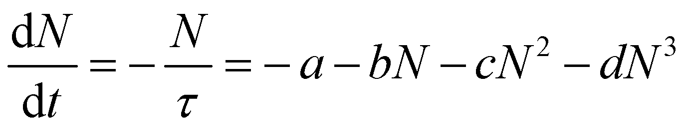 . We note that the equation ignores the diffusion of the carriers, as its rate is known to be much slower than the recombination.13 This equation consists of four terms, where the first and second terms correspond to the pseudo-first and first-order recombination of Shockley–Read–Hall (SRH) type, the third term is responsible for a radiative or bimolecular decay and the fourth term describes Auger recombinations, respectively. The coefficients depict the weight or rate constants for each process. However, we found that to model the data only the first term is necessary to describe the decay in the hydrogenated samples, while for the oxidised samples the recombination is almost exclusively governed by the third-order dependence on N, that is the fourth term in the differential equation. The corresponding fitting is shown by the solid lines in Fig. 2.
The recombination constants, a and d, (obtained from the fitting) were correlated with the morphological parameters of the samples. We found that, contrary to intuition, for porous silicon, these constants do not scale with the surface-to-volume ratio. A careful analysis of the data revealed that the scaling is rather governed by the inverse volume of the nano-crystalline silicon grains constituting the sponge scaffold, regardless of the chemical composition of the passivation.
To demonstrate this, we determined the effective energy gap, Eg, from Tauc plots, for which absorbance coefficient, α, evaluated from the transmittance and reflectance spectra, is plotted as 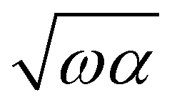 as a function of photon energy ħω. The Tauc plots and Eg corresponding for every sample are shown in Fig. S2 (ESI†). We found that, for the hydrogenated samples the energy gap, Eg, is systematically blue-shifted from ∼1.2 eV to ∼1.4 eV as the porosity increases from f = 0.66 to f = 0.88. A similar shift was observed for the samples which were oxidised following the hydrogenation. In addition, for the oxidised samples, we found that their energy gap is systematically larger than for the hydrogenated ones at a given porosity. This oxidation related blue-shift indicates that the size of silicon grains shrinks and the confinement of the charge-carriers increases as the hydrogen-related bonds are replaced by the oxide. The insets to Fig. 3 show that, Eg, established from Tauc plots, correlates linearly with the fractional volume of silicon nano-crystalline grains in porous silicon, 1 − f.
 | ||
| Fig. 3 Scaling of decay constant in hydrogenated and oxidised silicon nanocrystals. 1/τ, as a function of the inverse volume, 1/a3, of hydrogenated (a) and oxidised (b) nanocrystals. Insets show the evolution of pSi effective energy gap as the fractional volume, 1 − f, of silicon nano-crystalline grains increases. | ||
To estimate the radius of the nanocrystals, a, we used the approximation of the quantum confinement for a particle-in-a-sphere: Eg = ESig + ħ2βl,n2/2μmea2, where ESig = 1.12 eV is the band gap of bulk silicon, βl,n is the dual-index root of the spherical Bessel function, with l = 0 and n = 1 denoting the orbital and radial quantum numbers for the lowest state, and μ = 0.17 and me are the fractional electron/hole reduced and free electron masses, respectively.14 The right-hand ordinate axes of the insets represent the estimation of the mean nanocrystals radius, a.
Using the size of the nanocrystals for the range of the samples in this work, we collate the decay constants evaluated from the data in Fig. 2 and show in Fig. 3 that 1/τ scales as 1/a3, regardless of the chemical composition of the surface passivation and involved recombination process, i.e. either SRH or Auger scales with an inverse volume. Indeed, Fig. 3 shows that for the hydrogenated samples, where the main recombination process is attributed to SRH, the rate increases linearly with the inverse volume of the crystals. The same scaling phenomenon is observed for the oxidised samples, yet, in contrast, the main mechanism is Auger recombination and the rate is nearly two orders of magnitude faster.
Linear scaling of Auger recombination with 1/a3 in nanocrystals was previously demonstrated for a range of direct and indirect gap semiconductors22–25 and became central to the proposition of a Universal Size-Dependent Trend.12 However, this has not been explicitly demonstrated for silicon. The main attribute of the Trend is that it negates exponential dependence of the recombination rate on (−Eg), but rather follows 1/a3 spatial confinement. In addition, it suggests a relaxation of the momentum-conservation rule and diminishes the requirement to involve a momentum-matching phonon in indirect semiconductors.
In fact, our work supports the Trend for nanocrystals in porous silicon. In contrast to bulk semiconductors’ behaviour and in line with the Trend, Fig. 3 shows that the rate constant, 1/τ, increases when Eg increases and the size of nanocrystals decreases as 1/a3. Although the Trend is useful to predict the recombination rate in semiconducting nanocrystals, its essential attribute is rather empirical and it does not reveal the underlying mechanism. This work attempts to fill the lacunae, at least for silicon nanocrystals.
It has been shown in the previous works on nano-porous silicon that resonant excitation of vibrational modes of surface adsorbates by a probe beam induces Auger recombination, while for off-resonance probing the relaxation proceeds by the way of an SRH process.13 In this work, the probe beam wavelength does not coincide with any of the IR-active modes of the surface-adsorbates for the hydrogenated and oxidised passivation, and, Auger recombination is not expected. Indeed, this work confirms SRH as the main recombination channel in the hydrogenated samples. However, the question which requires elaboration is why replacing hydride with oxide bonds on the surface of the pores completely changes the recombination mechanism.
It is a well-established fact that Auger recombination in bulk silicon, in particular in its p-type, requires the assistance of phonons, helping to overcome the ∼76 meV barrier and matching the momentum conservation conditions (see ESI,† Fig. S3 for the barrier definition). Although a phonon assisted process is of the second order or higher, it reduces the barrier and overpowers pure Auger.15,26,27 On the other hand, for silicon nanocrystals, the confinement of the recombining charges increases the crystal-momentum uncertainty and relaxes the conservation rule, diminishing the dependence on the phonons. However, this effect is of importance for the confinement energies above 0.7 eV,28 decidedly higher than in our samples. Thus, we may safely assume that Auger recombination in our samples follows the same energy-momentum conservation scheme as in the bulk of p-type silicon with the participation of the combination of the TO and TA phonons with 57 and 18 meV energy, respectively, in the Γ–Δ direction.29,30 The combinations of the TA + TO or 2TO are sufficient to overcome the barrier and are known to be particularly active in the electron-hole recombination process.28 These phonons are known to be resonatively coupled to the Si–O stretching mode,31 which is abundant and strong in the oxidised samples (see Fig. 1). Thus, even at the room temperature, the surface passivation provides a rich source of the phonons needed to promote Auger recombination.
On the other hand, these phonon modes are unlikely to couple to Sin–Si–Hy vibrations in the hydrogenated samples. The wagging vibrations can be energetically matched by the phonons, but such coupling is suppressed as it would lead to broken symmetry. The stretching vibration satisfies the symmetry rules, but those are energetically too high for silicon phonons. Hence, the surface hydrogenation does not support conditions for phonon-assisted Auger recombination. Instead, the hydrogenated surface provides states for SRH mechanism. These are in-gap states which have been investigated in the previous works on hydrogenated amorphous and nano-crystalline silicon.32,33 It has been shown that these states do not disappear with the hydrogenation as they are attributed to the structural defects,11 related to the angular distortion of Si–Si bonds creating impurity-like localised electronic states.34 Indeed, this work in Fig. S2(d)–(f) shows that in either type of the surface passivation the in-gap states extend their presence by ∼0.2 eV below the Tauc gap.
Thus, we can summarise that in the oxidised samples a highly efficient coupling of phonons to surface vibrations modes of Si–O bonds promotes a very fast Auger process which overcomes competition with a slower SRH recombination involving structural defects states. In the hydrogenated samples, the resonative coupling between phonons and chemical adsorbates vibrations is absent and the recombination proceeds entirely through the SRH channel.
Methods
Sample preparation
The pSi samples used in this work were fabricated through the electrochemical anodisation process. The resistivity of a boron-doped silicon wafer, used in this work, was 0.005–0.02 Ohm cm, corresponding to a carrier concentration of about 1018 cm−3. The bulk silicon substrate was immersed into an electrolyte which is a mixture of ethanol and 40% hydrofluoric acid (HF) (ratio 1![[thin space (1/6-em)]](https://www.rsc.org/images/entities/char_2009.gif) :1). A DC voltage is then applied between the anode and cathode to accelerate the reaction between HF and silicon. The dissolution of silicon is caused by the replacement of silicon–hydrogen bonds by silicon–fluorine bonds on the surface. Pores are formed as the reaction products SiF4 and H2SiF6 are soluble in the electrolyte. By varying the electrolyte concentration and the current density, the porosity was tuned from 66 to 88%, while the thickness of ∼120 μm was controlled by the anodisation time. The separation of pSi from its bulk substrate was realised by applying a short current pulse with the current density of 120 mA cm−2 at the end of the anodisation. Under this current density, pores collapse at the boundary between pSi and Si resulting in the partition of the pSi layer. Brunauer–Emmett–Teller (BET) analysis was performed to determine the surface area, pore diameter and volume of the samples with different porosity, and the results are summarised in Table 1. The oxidation of pSi was carried out under 600 °C in an oven with a constant flow of oxygen and inert gases for 30 minutes. The samples were then left in the oven for 5 hours to gradually cool down in order to prevent the collapse of pSi structure due to the sudden change in temperature. The re-hydrogenation of samples was accomplished by dipping the oxidised samples in 10% HF solution for 30 seconds. Afterwards, the samples were rinsed in ethanol and stored in a box purged with nitrogen gas. Although one can argue that a longer time in HF might further remove the remaining Si–O–Si and dangling bonds, we observed that extended etching increased porosity and affected the recombination rate. Yet, re-oxidation still occurred during rinsing and air storage prior to characterization and during FTIR/optical measurements. This issue would not be eliminated by longer times in HF.
:1). A DC voltage is then applied between the anode and cathode to accelerate the reaction between HF and silicon. The dissolution of silicon is caused by the replacement of silicon–hydrogen bonds by silicon–fluorine bonds on the surface. Pores are formed as the reaction products SiF4 and H2SiF6 are soluble in the electrolyte. By varying the electrolyte concentration and the current density, the porosity was tuned from 66 to 88%, while the thickness of ∼120 μm was controlled by the anodisation time. The separation of pSi from its bulk substrate was realised by applying a short current pulse with the current density of 120 mA cm−2 at the end of the anodisation. Under this current density, pores collapse at the boundary between pSi and Si resulting in the partition of the pSi layer. Brunauer–Emmett–Teller (BET) analysis was performed to determine the surface area, pore diameter and volume of the samples with different porosity, and the results are summarised in Table 1. The oxidation of pSi was carried out under 600 °C in an oven with a constant flow of oxygen and inert gases for 30 minutes. The samples were then left in the oven for 5 hours to gradually cool down in order to prevent the collapse of pSi structure due to the sudden change in temperature. The re-hydrogenation of samples was accomplished by dipping the oxidised samples in 10% HF solution for 30 seconds. Afterwards, the samples were rinsed in ethanol and stored in a box purged with nitrogen gas. Although one can argue that a longer time in HF might further remove the remaining Si–O–Si and dangling bonds, we observed that extended etching increased porosity and affected the recombination rate. Yet, re-oxidation still occurred during rinsing and air storage prior to characterization and during FTIR/optical measurements. This issue would not be eliminated by longer times in HF.
| Porosity (%) | Surface area (m2 g−1) | Pore diameter (nm) | Pore volume (ml g−1) |
|---|---|---|---|
| 66.4 | 258.60 | 12.33 | 0.79 |
| 67.4 | 277.20 | 12.94 | 0.89 |
| 70.7 | 292.40 | 11.38 | 1.04 |
| 79 | 359.75 | 13.20 | 1.53 |
| 83.8 | 420.48 | 17.00 | 2.25 |
| 87.5 | 457.64 | 21.46 | 3.01 |
VIS-NIR and FTIR spectrum measurements
The Tauc plots used for the band-gap estimation were obtained from the transmission and reflection spectrum in the wavelength range of 500–2500 nm. A broadband unpolarized white light source was used to illuminate the samples, while the transmitted and reflected light was collected by a PerkinElmer Lambda 1050 UV/Vis/NIR spectrometer. A Bruker FTIR Hyperion microscope was used for the FTIR measurements. A 50× objective was used to focus the IR beam on the sample. The transmission spectrum was obtained by averaging the measurements of five random spots of each sample. We confirmed that the samples have excellent uniformity and the uncertainty on transmission spectra was less than 1%. The main IR active modes observed in our experiments are summarised in Table 2. Note that relatively high doping contributes to the featureless background arising from the free carrier absorption. It can be estimated that ∼20% of the incoming IR light is absorbed traversing the 120 μm-thick samples with the absorption coefficient of ∼70 cm−1 in this range.13| Vibrational | Mode | Wavenumber (cm−1) |
|---|---|---|
| SiO–H | Stretching | ∼3700 |
| OySi–Hx | Stretching | ∼2200 |
| Sin–Si–Hy | Stretching | ∼2100 |
| SiO–H | Bending | ∼1650 |
| Si–O–Si | Stretching | ∼1100 |
| Si2–Si–H2 | Scissor | ∼900 |
| Sin–Si–Hy | Wagging | ∼600–715 |
Time-resolved pump–probe measurements
The time-resolved change of transmittance measurements were performed using an ultrafast laser system (Coherent Ltd). Intensive fundamental laser pulses (average power ∼3 W) with 800 nm central wavelength, 60 femtoseconds duration were produced by an Ti:sapphire amplifier.35 The smaller fraction of the beam (about 5%) was used as the pump beam to excite the free carriers in the pSi samples simultaneously. The remnant of the beam was guided into an optical parametric amplifier (OPerA-Solo) to generate a probe beam with a wavelength of 2.5 μm and pulse duration of about 200 femtoseconds.13 The optical path length of the pump beam was adjusted by a computer-controlled retroreflector to scan the temporal overlap between the pump and probe on the sample. To ensure spatially homogeneous excitation, the pump beam spot diameter on the sample was adjusted to 1 mm and the probe spot diameter was set to 500 μm. Both the pump and probe intensity were controlled by rotating half-wave plates in front of linear polarisers which also set the beam polarisation. The pump beam was set to p-polarised, while the probe beam was adjusted to be orthogonally polarised with respect to the pump to prevent interference between them. The incident angle of the pump was set to 30° while the probe beam was incident perpendicular to the sample surface. The transient transmission of the probe beam was detected by a PbS detector, which was connected to a lock-in amplifier (Zurich Instrument). The recorded data was read out by a LabVIEW program.Author contributions
A. K. conceived the experiments, R. W. and J. C. conducted the experiments, E. N., C. J. S. and L. C. fabricated the samples; R. W. and M. N. analysed the results. All authors participated in the writing and reviewing of the manuscript.Conflicts of interest
There are no conflicts to declare.Acknowledgements
J. C. thanks Dstl for financial support enabled by the grant DSTLX100099482. M. N.-C. acknowledges support from European Union Horizon 2020 research and innovation programme (Grant No. 777714). A. K. thanks the Engineering and Physical Sciences Research Council for financial support (Grant number EP/V000055/1; Metal Atoms on Surfaces and Interfaces for Sustainable Future).References
- L. T. Canham, Silicon quantum wire array fabrication by electrochemical and chemical dissolution of wafers, Appl. Phys. Lett., 1990, 57, 1046–1048 CrossRef CAS.
- V. Lehmann and U. Gösele, Porous Si formation: A quantum wire effect, Appl. Phys. Lett., 1991, 58, 856–858 CrossRef CAS.
- V. Robbiano, G. M. Paternò, A. A. La Mattina, S. G. Motti, G. Lanzani, F. Scotognella and G. Barillaro, Room-temperature low-threshold lasing from monolithically integrated nanostructured porous silicon hybrid microcavities, ACS Nano, 2018, 12, 4536–4544 CrossRef CAS PubMed.
- S. J. Park, A. Zakar, V. L. Zerova, D. Chekulaev, L. T. Canham and A. Kaplan, All-optical modulation in mid-wavelength infrared using porous Si membranes, Sci. Rep., 2016, 6, 30211 CrossRef CAS PubMed.
- L. Khriachtchev, Silicon Nanophotonics: Basic Principles, Present Status and Perspectives, World Scientific, Singapore, 2008 Search PubMed.
- K. Kim and T. E. Murphy, Porous silicon integrated mach-zehnder interferometer waveguide for biological and chemical sensing, Opt. Express, 2013, 21, 19488–19497 CrossRef PubMed.
- R. Wu, T. Mathieu, C. J. Storey, Q. Jin, J. Collins, L. T. Canham and A. Kaplan, Localized plasmon field effect of gold clusters embedded in nanoporous silicon, Adv. Opt. Mater., 2021, 9, 2002119 CrossRef CAS.
- R. Wu, Q. Jin, C. J. Storey, J. Collins, G. Gomard, U. Lemmer, L. T. Canham, R. Kling and A. Kaplan, Gold nanoplasmonic particles in tunable porous silicon 3D scaffolds for ultra-low concentration detection by SERS, Nanoscale Horiz., 2021, 6, 781–790 RSC.
- S. Öğüt, J. R. Chelikowsky and S. G. Louie, Quantum confinement and optical gaps in Si nanocrystals, Phys. Rev. Lett., 1997, 79, 1770–1773 CrossRef.
- G. Hadjisavvas and P. C. Kelires, Structure and energetics of Si nanocrystals embedded in a –SiO2, Phys. Rev. Lett., 2004, 93, 226104 CrossRef CAS PubMed.
- S. Godefroo, M. Hayne, M. Jivanescu, A. Stesmans, M. Zacharias, O. I. Lebedev, G. Van Tendeloo and V. V. Moshchalkov, Classification and control of the origin of photoluminescence from Si nanocrystals, Nat. Nanotechnol., 2008, 3, 174–178 CrossRef CAS PubMed.
- I. Robel, R. Gresback, U. Kortshagen, R. D. Schaller and V. I. Klimov, Universal size-dependent trend in auger recombination in direct-gap and indirect-gap semiconductor nanocrystals, Phys. Rev. Lett., 2009, 102, 177404 CrossRef PubMed.
- A. Zakar, R. Wu, D. Chekulaev, V. Zerova, W. He, L. T. Canham and A. Kaplan, Carrier dynamics and surface vibration-assisted auger recombination in porous silicon, Phys. Rev. B: Condens. Matter Mater. Phys., 2018, 97, 155203 CrossRef CAS.
- W. He, A. Zakar, T. Roger, I. V. Yurkevich and A. Kaplan, Determination of recombination coefficients for nanocrystalline silicon embedded in hydrogenated amorphous silicon, Opt. Lett., 2015, 40, 3889–3892 CrossRef CAS PubMed.
- A. Haug, Auger recombination with deep impurities in indirect band gap semiconductors, Phys. Status Solidi B, 1981, 108, 443–448 CrossRef CAS.
- W. Theiß, Optical properties of porous silicon, Surf. Sci. Rep., 1997, 29, 91–192 CrossRef.
- H. Hövel, P. Grosse and W. Theiss, Analysis of photoacoustic IR spectra of aerogel and silica powder, J. Non-Cryst. Solids, 1992, 145, 159–163 CrossRef.
- D. B. Mawhinney, J. A. Glass and J. T. Yates, FTIR study of the oxidation of porous silicon, J. Phys. Chem. B, 1997, 101, 1202–1206 CrossRef CAS.
- T. Seki, K.-Y. Chiang, C.-C. Yu, X. Yu, M. Okuno, J. Hunger, Y. Nagata and M. Bonn, The bending mode of water: A powerful probe for hydrogen bond structure of aqueous systems, J. Phys. Chem. Lett., 2020, 11, 8459–8469 CrossRef CAS PubMed.
- P. Kumar, T. Hofmann, K. Knorr, P. Huber, P. Scheib and P. Lemmens, Tuning the pore wall morphology of mesoporous silicon from branchy to smooth, tubular by chemical treatment, J. Appl. Phys., 2008, 103, 024303 CrossRef.
- W. He, R. Wu, I. V. Yurkevich, L. T. Canham and A. Kaplan, Reconstructing charge-carrier dynamics in porous silicon membranes from time-resolved interferometric measurements, Sci. Rep., 2018, 8, 17172 CrossRef PubMed.
- V. I. Klimov, A. A. Mikhailovsky, D. W. McBranch, C. A. Leatherdale and M. G. Bawendi, Quantization of multiparticle auger rates in semiconductor quantum dots, Science, 2000, 287, 1011–1013 CrossRef CAS PubMed.
- R. D. Schaller and V. I. Klimov, High efficiency carrier multiplication in PbSe nanocrystals: Implications for solar energy conversion, Phys. Rev. Lett., 2004, 92, 186601 CrossRef CAS PubMed.
- R. D. Schaller, J. M. Pietryga and V. I. Klimov, Carrier multiplication in InAs nanocrystal quantum dots with an onset defined by the energy conservation limit, Nano Lett., 2007, 7, 3469–3476 CrossRef CAS PubMed.
- V. I. Klimov, J. A. McGuire, R. D. Schaller and V. I. Rupasov, Scaling of multiexciton lifetimes in semiconductor nanocrystals, Phys. Rev. B: Condens. Matter Mater. Phys., 2008, 77, 195324 CrossRef.
- A. Haug, Carrier density dependence of auger recombination, Solid-State Electron., 1978, 21, 1281–1284 CrossRef.
- D. B. Laks, G. F. Neumark and S. T. Pantelides, Accurate interband-auger-recombination rates in silicon, Phys. Rev. B: Condens. Matter Mater. Phys., 1990, 42, 5176 CrossRef CAS.
- D. Kovalev, H. Heckler, M. Ben-Chorin, G. Polisski, M. Schwartzkopff and F. Koch, Breakdown of the k-conservation rule in Si nanocrystals, Phys. Rev. Lett., 1998, 81, 2803–2806 CrossRef CAS.
- O. J. Glembocki and F. H. Pollak, Relative intensities of indirect transitions: Electron–phonon and hole–phonon interaction matrix elements in Si (TO) and GaP (LA,TA), Phys. Rev. B: Condens. Matter Mater. Phys., 1982, 25, 1193–1204 CrossRef CAS.
- O. J. Glembocki and F. H. Pollak, Calculation of the – electron-phonon and hole-phonon scattering matrix elements in silicon, Phys. Rev. Lett., 1982, 48, 413–416 CrossRef CAS.
- M. Pradhan, R. Garg and M. Arora, Interaction of oxygen and carbon impurities with the multiphonon infrared absorption bands of silicon at low temperatures, Infrared Phys., 1987, 27, 207–213 CrossRef CAS.
- E. Fefer, Y. Shapira and I. Balberg, Direct determination of the band gap states in hydrogenated amorphous silicon using surface photovoltage spectroscopy, Appl. Phys. Lett., 1995, 67, 371–373 CrossRef CAS.
- D. Cavalcoli, M. Rossi and A. Cavallini, Defect states in nc-Si:H films investigated by surface photovoltage spectroscopy, J. Appl. Phys., 2011, 109, 053719 CrossRef.
- L. Bagolini, A. Mattoni and L. Colombo, Electronic localization and optical absorption in embedded silicon nanograins, Appl. Phys. Lett., 2009, 94, 053115 CrossRef.
- A. Kaplan, M. Lenner, C. Huchon and R. E. Palmer, Nonlinearity and time-resolved studies of ion emission in ultrafast laser ablation of graphite, Appl. Phys. A: Mater. Sci. Process., 2008, 92, 999–1004 CrossRef CAS.
Footnote |
| † Electronic supplementary information (ESI) available: Methods.pdf. See DOI: https://doi.org/10.1039/d2cp00325b |
| This journal is © the Owner Societies 2022 |