
Electronic structures of Zn1−xGaxO1−xNx and band offsets of the ZnO/Zn1−xGaxO1−xNx heterojunction across the entire concentration range from first principles†
Tianjiao
Li
a,
Xiaojie
Liu
*a,
Yin
Wang
 *b,
Ronggen
Cao
c and
Haitao
Yin
*a
*b,
Ronggen
Cao
c and
Haitao
Yin
*a
aKey Laboratory for Photonic and Electronic Bandgap Materials of Ministry of Education, School of Physics and Electronic Engineering, Harbin Normal University, Harbin 150025, China. E-mail: redlxj@126.com; wlyht@126.com
bDepartment of Physics and International Centre for Quantum and Molecular Structures, Shanghai University, Shanghai 200444, China. E-mail: yinwang@shu.edu.cn
cDepartment of Materials Science, Fudan University, Shanghai 200433, China
First published on 26th November 2021
Abstract
Band offsets at the heterointerfaces play a key role in defining the functionality of optoelectronic devices. In this work, the band gaps of wurtzite Zn1−xGaxO1−xNx alloys and the band offsets of the lattice matched ZnO/Zn1−xGaxO1−xNx heterojunction across the entire concentration range of GaN were investigated by the modified Becke–Johnson (mBJ) semi-local exchange combined with the coherent potential approximation (CPA). The calculated band gaps of Zn1−xGaxO1−xNx alloys can be tuned by the concentration of the doping GaN and show a strong band gap bowing. The heterojunctions ZnO/Zn1−xGaxO1−xNx form either type I or type II band alignment by adjusting the concentration of GaN; especially, when the concentration is in the range of 0.8 < x < 0.97, the band gaps of Zn1−xGaxO1−xNx cover visible light, and the heterojunctions show type II band alignment, which would help to enhance the solar light adsorption ability and improve the carrier collection efficiency in the design and optimization of ZnO and GaN-based heterojunctions for the applications of optoelectronics and photocatalysis.
1. Introduction
Water splitting into gaseous oxygen and hydrogen using semiconductor-based photocatalysts is one of the most promising technologies for producing cleaner and more sustainable chemical fuel.1 The ideal photocatalytic materials for harvesting solar energy should have the proper band gaps to cover the broadband of the solar spectra, which will produce high solar to energy conversion rate. For traditional photocatalytic materials such as TiO2 and ZnO, the conversion rate is usually very lower because of their large band gaps (3.2 eV for TiO22 and 3.37 eV for ZnO3), which makes them only responsive to ultraviolet irradiation and blind to visible and infrared irradiation.To achieve better catalytic effects in water splitting, many novel visible light responsive photocatalysts have been fabricated successfully using band structure engineering.4,5 For ZnO, the nitrogen atom is considered as the best candidate for a dopant because its ionic radius is the same as that of oxygen and the N-doping could result in the minimum strain in ZnO. The experimental result also shows that the N doping improved effectively the light absorption in the visible range.6 Of particular interest is the Ga–N codoping, which has been proposed to realize visible light responsive photocatalysts. For instance, GaN:ZnO solid solution as a stable photocatalyst for the overall cleavage of water has been synthesized.7 In this regard, the compound, Zn1−xGaxO1−xNx, whose energy bandgaps can be continuously tuned across the entire solar spectrum, is desirable. In the last decade, various synthesis routes have been used to fabricate the Zn1−xGaxO1−xNx alloy to meet the specific needs of different applications.8,9 Meanwhile, various approach-based density functional theory (DFT) has been employed to study the origin and characteristics of the reduction of the alloy. Muhammad N. Huda et al. revealed an asymmetric bandgap reduction in this nonisovalent system.10 V. S. Olsen et al. found that the defect band at the top of the valence band maximum causes the energy gap bowing in (ZnO)1−x (GaN)x alloys.11 L. L. Jensen et al. pointed out that the bowing of the band gap over the entire composition range is downward for (Ga1−xZnx)(N1−xOx) and the minimum band gap is estimated to be about 2.29 eV for the intermediate concentration x = 0.525 with the DFT+U approach.12 Also, the band gap bowing of the alloys was investigated through the partial self-consistent GW approximation13 and the strong repulsion between the Zn 3d and N 2p states and type II band alignment of ZnO/GaN were suggested as possible explanations of bandgap behavior.14,15 But the quantitative relationship of the bandgap of Zn1−xGaxO1−xNxversus any doping concentration, and how much doping concentration can adjust the band gap to the visible light range are still lacking.
Another major factor to influence photocatalytic efficiency is the low separation rate of the photo excited electrons and holes in ZnO. A large proportion of photogenerated carriers are recombined at the surface or in the interior of the semiconductor, emanating in the form of light and heat, and this part of the energy is not effectively utilized. The composite semiconductor photocatalysts have proven to be very effective for expanding the photo absorption range and facilitating the separation of the photo-generated carriers. Recently, a large number of photocatalysts based on the ZnO heterojunction have been synthesized to enhance photocatalytic efficiency, such as ZnO/ZnSe,16 ZnO/In2S3,17 ZnO/CdTe,18 and TiO2/ZnO.19 However, in these heterostructures, the lattice mismatch of coupled semiconductors is larger than 18%. Many lattice defects will be induced at the interface of heterostructures,20 resulting in recombination centers for electron–hole pairs, which straightly restrict the further application of these heterostructures.
The wurtzite ZnO, GaN as well as their compounds Zn1−xGaxO1−xNx have very close lattice parameters.21 Heterojunctions with type II band alignment have the natural property of separating carriers. Theoretical calculation and experimental study showed that ZnO can form type-II band alignment with GaN.22–24 Moreover, Z. Wang et al. found that the (Ga0.875Zn0.125)(N0.875O0.125) alloy can also form type-II band alignment with both GaN and ZnO from first principles calculation.25 The heterojunctions composed of Zn1−xGaxO1−xNx, ZnO and GaN, even multi-junctions of a single material family Zn1−xGaxO1−xNx, where each junction is associated with different bandgaps to cover a wider region of the solar spectrum, may produce the highest energy conversion efficiency in photovoltaic devices. Up to now, there is still lack of the band-line-up data for these heterojunctions at arbitrary concentration, which are highly needed in optoelectronic device application and design.
In this work, we apply DFT under the linear muffin-tin orbital (LMTO) scheme, to investigate the bandgaps of the Zn1−xGaxO1−xNx and band offsets of its heterojunctions. The modified Becke–Johnson (mBJ) semilocal exchange potential was employed to obtain the correct bandgap and coherent potential approximation (CPA) to simulate the different concentration doping. Under the frame of DFT-LMTO-mBJ-CPA, we can do direct DFT analysis of electronic structure of doping semiconductor and its heterojunction, avoiding very large supercells to simulate the low concentration doping and extremely expensive calculation cost for advanced methods.11,12 This method has been successful in calculating the electronic structure of many semiconductors,26 their alloys27,28 and heterojunctions.29,30 The calculated results were quantitatively coincident with the measured data.
2. Calculation method and details
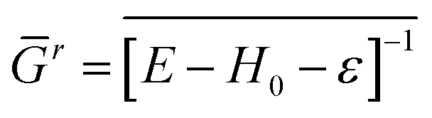
In our calculations, the DFT-LMTO-mBJ-CPA self-consistent approach, as implemented in the NANODSIM software package,31 was employed. At the atomic sphere approximation (ASA),32,33 one should put some vacancy spheres at proper locations for space filling and optimize the sphere radii to reproduce the correct electronic structure34 (ASA of ZnO and GaN are given in the ESI†). To handle the disorder impurity or doping in the medium, CPA was applied.35,36 Here, a brief introduction of the CPA is presented. Suppose the site i has xiq probability to be atom q. The retarded Green's function of the medium reads| Gr = [E − H0 − ε]−1 | (1) |
 | (2) |
![[small epsilon, Greek, tilde]](https://www.rsc.org/images/entities/i_char_e0de.gif) i}, called coherent potential, was introduced to replace the random onsite energy {i} such that the average scattering vanishes with respect to the effective media. Thus, the disorder average can be evaluated by
i}, called coherent potential, was introduced to replace the random onsite energy {i} such that the average scattering vanishes with respect to the effective media. Thus, the disorder average can be evaluated by| Ḡr = [E − H0 − ]−1 | (3) |
 | (4) |
i can be iteratively solved from above eqn (3) and (4), and Ḡr can be also yielded. Therefore, the electronic properties of a disordered system can be handled in a very small unit cell. Low computational load of the CPA greatly promotes the high-throughout calculation from first principles, although the local lattice distortion induced by solutes is not considered. Another approach special quasi-random structures (SQS)37,38 can treat the composition disorder in solid solutions, in which the local lattice distortion effect is considered. The disadvantage of SQS is that a large supercell is also needed. The atomic position relaxation makes the calculations often cumbersome.
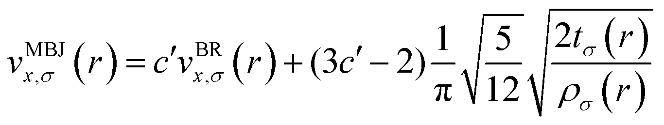
The mBJ potential was used to accurately calculate the bandgaps of the semiconductors, which has the following form39,40
 | (5) |
The primitive cells were used to obtain the electronic structure of the Zn1−xGaxO1−xNx alloy, and the supercell systems containing five cell layers of pure ZnO and five cell layers of Zn1−xGaxO1−xNx alloy to obtain the potential profile of the heterojunction. The schematic atomic structure of the heterojunction is shown in Fig. 1. In self-consistent calculations, a 9 × 9 × 5 k-mesh for the primitive cells and a 5 × 5× 2 k-mesh for the heterojunctions were used to sample the Brillouin zone, respectively. In addition, the experimental lattice constants, a = 3.2495 Å, c/a = 1.60247, and μ = 0.382c of wurtzite ZnO,42,43 were used for pure ZnO and its alloys.
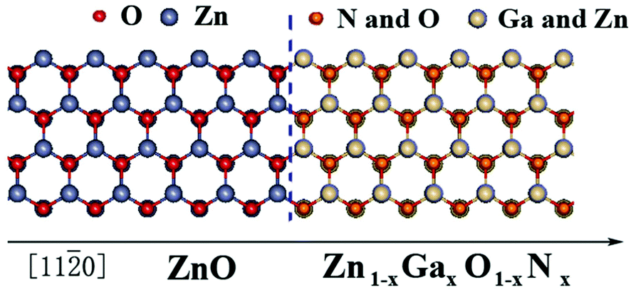 | ||
| Fig. 1 Schematic atomic structure of the ZnO/Zn1−xGaxO1−xNx heterojunction. | ||
3. Results and discussion
To intuitively display the band profile, we calculated the spectral function of the alloys (also called CPA band), which is a function of both energy E and momentum k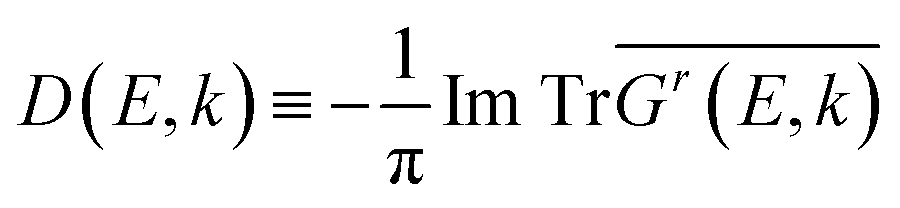 | (6) |
 denotes the disorder average of retarded Green's function. CPA band can provide rich and more accurate band information for the alloys than density of states (DOS). As mentioned before, by adjusting the c′-parameters and using the mBJ potential, we obtained the band structures of ZnO and GaN, which have band gaps of 3.37 eV and 3.47 eV as shown in Fig. 1(a) and (d). Introducing the randomly distributed GaN dopant in the ZnO host significantly reduces the band gap. For example, when the concentration x is 0.01, the bandgap is 2.43 eV, and when x = 0.94, the bandgap is 2.82 eV, as shown in Fig. 2(b) and (c). The experimental gap of 6% ZnO concentration in the GaN host is 2.77 eV,44 and the gap of 5% is 2.8 eV,45 which is in good agreement with our calculated result.
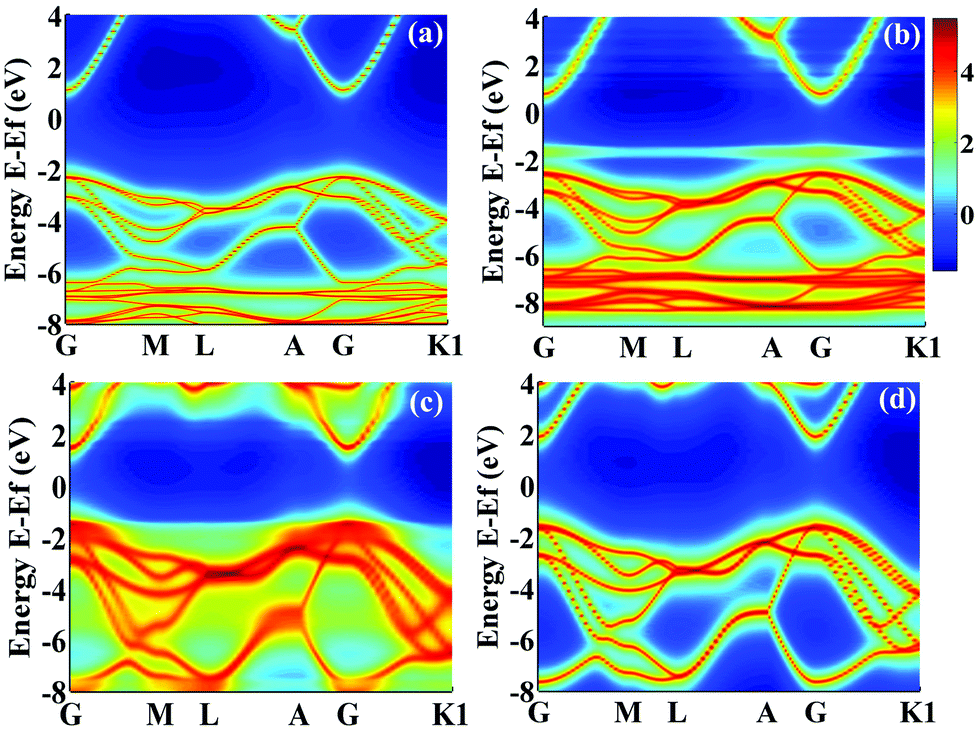 | ||
| Fig. 2 Calculated CPA band structure. (a) ZnO, (b) Zn0.99Ga0.01O0.99N0.01, (c) Zn0.06Ga0.94O0.06N0.94, and (d) GaN with the bandgaps of 3.37 eV, 2.43 eV, 2.82 eV and 3.47 eV, respectively. The calculated CPA bands were in logarithmic scale to get a better look. The different colors represent the value of the D(E,k) at different E and k. | ||
Using the DFT-LMTO-mBJ-CPA method, we calculated the bandgaps of Zn1−xGaxO1−xNx alloys across the entire concentration range. The results are plotted in Fig. 3. The bandgaps versus concentrations have the following features: (1) the bandgaps of the Zn1−xGaxO1−xNx alloy are smaller than that of either ZnO or GaN, and the overall trend over entire concentration is downward first, and then upward; (2) the trend of the change of the reduction shows asymmetric behavior:10 the band gap decreases suddenly at the initial stages of the alloying (x < 0.001), followed by parabolic type, and terminated by linearity at about x > 0.8. The overall trend is similar to that of the special-quasi-random structure method;14 (3) it is more effective gap reduction for GaN doping in the host ZnO than ZnO doping in the host GaN; (4) the minimum bandgap is estimated to be about 1.49 eV at x = 0.40, which is coincident with the results by HSE (1.45 eV) and GW (1.66 eV) methods,13 but the calculated minimum bandgap value is lower than the experimental value.46 The calculated concentration corresponding to the minimum gap is lower than that of, ref. 12 where they speculated x = 0.475 employing the GGA+U approach.
 | ||
| Fig. 3 Bandgaps of the Zn1−xGaxO1−xNx alloy vs. the GaN component. Asterisks are calculated data and the solid line is the fitting of the theoretical results with a bowing parameter of 7.40 eV. Inset: Gap versus x in the low concentration range. | ||
The conventional bowing formula, which only involves a single bowing parameter, cannot correctly represent the relation between the bandgaps and the composition across the entire concentration range. When the concentration is between 0.5 and 1.0, the alloys have a strong bandgap bowing. By fitting the calculated data onto the expression Eg(Zn1−xGaxO1−xNx) = (1 − x)Eg(ZnO) + xEg(GaN) − bx(1 − x), the obtained bowing parameter b is 7.40 eV, which is consistent with the value of 7.31 eV from the GW method.13 But when the concentration is low, the fitting curve obviously deviated from the theoretical values. The deviation comes from the fact that the doping of GaN introduces impurity states inside the ZnO bandgap, as shown in Fig. 2(b). The impurity states lead to the significant and sudden reduction of the bandgap even the concentration is very low. The situation is different from the reduction of high concentration as shown in Fig. 2(c), where there is no impurity state in the gap. These different bandgap reducing mechanisms at low and high concentrations make it hard to estimate this distinct band bowing via a conventional single bowing parameter formula.
To understand more about the above significant gap reduction and reveal how atoms interact in Zn1−xGaxO1−xNx, we calculated the projection density of states (PDOS) on each atom at different concentrations. Fig. 4 displays the calculated PDOS of Zn1−xGaxO1−xNx alloys with x = 0, 0.01, 0.05. 0.95, 0.99, and 1.0. The pair of dashed vertical lines refers to the valence band maximum (VBM) and conduction band minimum (CBM) (i.e., Ev and Ec, respectively). The VBM of pure ZnO is taken as an energy reference. All PDOS are displayed for the energy range [−3 eV, +5 eV] in order to focus on the valence band and conduction band states near the bandgap. When the doping concentration of GaN is very low, the top of the VBM is mainly contributed by N atoms because N is less electronegative than O. The impurity level upshifts the VBM remarkably. At the same time, the CBM is down ward due to the decrease of the interaction of the cation Zn and anion O with the GaN doping. They result in the reduction of bandgaps of Zn1−xGaxO1−xNx together. For example, at the concentration of 0.01, the CBM is reduced about 0.06 eV and the VBM is raised about 0.88 eV compared to the pure ZnO, which leads to a net bandgap reduction of 0.94 eV, as shown in Fig. 4(b). With the increase of the GaN concentration x, for x = 0.05 as shown in Fig. 4(c), the width of the impurity state becomes wider, and the peak moves away from the original valence band slightly, and the CBM decreases gradually. Together these factors determine the further reduction of the bandgap. At about 40%, the bandgap arrives at the minimum value of 1.49 eV. When the doping concentration further increases, the bandgap begins to widen gradually. At last, the bandgap arrives at the maximum of 3.47 eV when x = 1.0. In other words, in the GaN host material, the bandgap also decreases with the increase of the concentration of randomly distributed ZnO. As shown in Fig. 4(e) and (f), the VBM is mainly contributed from the N atom and the CBM is mainly contributed from the Ga and Zn atoms. The possible reason maybe comes from the fact that when alloyed with ZnO, the repulsion between Zn-3d states, which are shallower than the Ga-3d states, and N-2p states in the valence bands causes the upshift of the VBM. Meanwhile, the bottom of conduction bands downshifts due to the interaction between O(N) and Ga (Zn). It should be noticed that compared to the experimental values11,47 the calculated gap is underestimated at high doping concentrations, which may originate from over hybridization between the Zn-3d states and the N-2p states, resulting in an artificial enhancement of the p–d electron repulsion.
 | ||
| Fig. 4 PDOS of Zn1−xGaxO1−xNx calculated from the ZnO/Zn1−xGaxO1−xNx heterojunction with (a) x = 0, (b) x = 0.01, (c) x = 0.05, (d) x = 0.95, (e) x = 0.99 and (f) x = 1.0. The black solid lines show the total DOS of Zn1−xGaxO1−xNx, the red solid lines represent the PDOS of the O and N atoms, and the blue solid lines are the PDOS of the Zn and Ga atoms, respectively. | ||
Having correctly determined the bandgaps of the Zn1−xGaxO1−xNx alloy and understood the microscopic origin of the bandgap reduction, we next investigated the band alignment of the lattice matched ZnO/Zn1−xGaxO1−xNx heterojunction. The valence band offset (VBO) and conduction band offset (CBO) of a heterojunction can be calculated as48–50
| VBO(CBO) = ΔEν(c) + ΔV | (7) |
The calculated band alignments and band offsets are shown in Fig. 5 and 6. Both VBO and CBO are sensitive to the concentration of the doping GaN. When the concentration is in the range of 0 < x < 0.8, the CBO is positive and VBO is negative, which means that the CBM of the ZnO is higher than that of the Zn1−xGaxO1−xNx and the VBM of ZnO is lower than that of Zn1−xGaxO1−xNx in energy. These two semiconductors form a heterojunction with type I band offset, in which both electrons and holes are confined in the Zn1−xGaxO1−xNx semiconductor. Such a structure with higher recombination rate of electrons and holes is desired in the field of light-emitting diodes or laser diodes. However, the concentration of GaN is larger than about 0.8, and both VBO and CBO are negative, which means that both the valence and conduction bands of ZnO lie lower than the corresponding bands of Zn1−xGaxO1−xNx, exhibiting type-II band offset features. The calculations also show that the CBO and VBO of the ZnO/GaN heterojunction are −0.77 eV and −0.87 eV, respectively. These results agree with the measured VBM of 0.9 ± 0.1 eV.51 Our calculated VBO for ZnO/GaN is also in good agreement with the quasiparticle self-consistent GW approach (0.7 eV)52 and the GGA+U method (0.7 eV).10
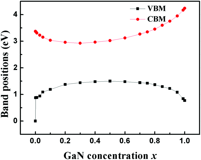 | ||
| Fig. 5 Band alignments as a function of GaN concentration x. Band positions are aligned to the edge of the VB of pure ZnO by heterojunction calculations. Black squares are the VBM and red dots are the CBM of Zn1−xGaxO1−xNx, respectively. | ||
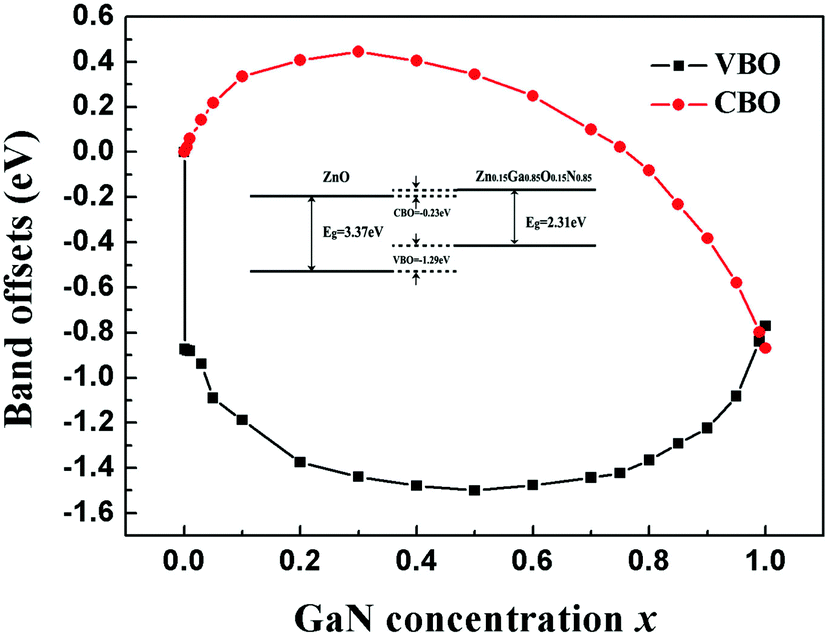 | ||
| Fig. 6 Band offsets of the ZnO/Zn1−xGaxO1−xNx heterojunctions. Black solid squares and red dots represent the VBO and CBO of the heterojunctions, respectively. The CBO (VBO) values are with respect to the CBM (VBM) of ZnO in units of eV. Inset: The band alignment diagram of the ZnO/Zn0.15Ga0.85O0.15N0.85 heterojunction. | ||
To enhance the visible light adsorption ability and improve the carrier collection efficiency in the ZnO/Zn1−xGaxO1−xNx heterojunction, GaN content must be controlled to be in a proper range. On the basis of the above calculations, we propose heterostructure photocatalysts composed of ZnO and Zn1−xGaxO1−xNx (0.8 < x < 0.97) to minimize the recombination of photo-generated electrons and holes, and then enhance the photocatalytic efficiency, as shown in Fig. 7. We introduce a Zn1−xGaxO1−xNx layer, whose bandgap is about between 2.09 eV and 3.05 eV, to increase the visible light adsorption. When the heterostructure is irradiated with solar light, the photo-generated electrons in the CB of Zn1−xGaxO1−xNx are then injected into the CB of ZnO. Simultaneously, the holes of the VB of ZnO are injected into the VB of Zn1−xGaxO1−xNx. Photogenerated electrons and holes flow in the opposite direction for appropriate VBO. Thus, the rate of spatial charge separation increases and the electron–hole pair recombination reduces accordingly in this heterojunction with type-II band offset. Moreover, our calculated band alignments are not only limited to the ZnO-based heterojunction. For example, if the heterojunction is composed of GaN and the compounds Zn1−xGaxO1−xNx (0.3 < x < 1), the CBM of GaN is always higher than that of Zn1−xGaxO1−xNx, but the VBM is just the opposite. This means that it is a type I band alignment heterojunction. Importantly, the narrower band gap can be continuously tuned from 1.49 eV to 3.47 eV, and the emission region covers the infrared, visible and ultraviolet, which is desired in design of LEDs or laser diodes.
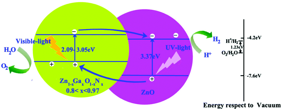 | ||
| Fig. 7 Proposed band structure of Zn1−xGaxO1−xNx/ZnO. The conduction band (CB) and the valence band (VB) of ZnO with respect to the vacuum level are located at −4.2 and −7.6 eV.42 | ||
Finally, it needs to be added that the band alignment we studied here is a static band alignment. The Fermi level equilibration across the interface of the heterojunction is not considered, although it may play an important role in the alignment of bands for heterojunctions and the direction of charge-flow.53 Moreover, neither of the two materials ZnO and Zn1−xGaxO1−xNx which make up the heterojunction contains any defect. The influence of defects on the band offsets of the heterojunction needs to be further studied.
4. Conclusion
Under the frame of DFT-LMTO-mBJ-CPA, we investigated the bandgaps of Zn1−xGaxO1−xNx and band offsets of the ZnO/Zn1−xGaxO1−xNx heterojunction for the entire doping concentration of GaN. Our results show that the bandgaps of Zn1−xGaxO1−xNx alloys can be tuned effectively by the concentration of the doping GaN and show strong bandgap bowing. The band alignment type and band offsets of the ZnO/Zn1−xGaxO1−xNx heterojunction are closely relevant to the concentration of the doping GaN. When the concentration is in the range 0 < x < 0.8, the ZnO/Zn1−xGaxO1−xNx heterojunction shows type I band alignment. If the concentration is in the range of 0.8 < x < 0.97, the bandgaps of Zn1−xGaxO1−xNx will cover the broadband of the solar spectra, and the ZnO/Zn1−xGaxO1−xNx heterojunction shows type II band alignment. Our calculated band alignment can help to design and optimize ZnO or GaN-based heterojunctions for the applications of photocatalysis and optoelectronics.Conflicts of interest
There are no conflicts to declare.Acknowledgements
This work was supported by the Natural Science Foundation of Heilongjiang Province, China (grant no. LH2020A013), the National Natural Science Foundation of China (grant no. 52071087) and the Education Commission Heilongjiang Province (grant no. 2020-KYYWF352). Haitao Yin thanks Li Niu for VASP calculation.Notes and references
- X. Chen, S. Shen, L. Guo and S. Mao, Chem. Rev., 2010, 110, 6503–6570 CrossRef CAS PubMed.
- H. Tan, J. Scott, Y. H. Ng and R. A. Taylor, ACS Catal., 2016, 6, 1870–1879 CrossRef.
- D. C. Reynolds, D. C. Look, B. Jogai, C. W. Litton, G. Cantwell and W. C. Harsch, Phys. Rev. B: Condens. Matter Mater. Phys., 1999, 60, 2340–2344 CrossRef CAS.
- B. Alotaibi, H. P. T. Nguyen, S. Zhao, M. G. Kibria, S. Fan and Z. Mi, Nano Lett., 2013, 13, 4356–4361 CrossRef CAS PubMed.
- S. Sunkara, V. K. Vendra, J. B. Jasinski, T. Deutsch, A. N. Andriotis, K. Rajan, M. Menon and M. Sunkara, Adv. Mater., 2014, 26, 2878–2882 CrossRef CAS PubMed.
- B. M. Rajbongshi, A. Ramchiary and S. Samdarshi, Mater. Lett., 2014, 134, 111–114 CrossRef CAS.
- K. Maeda, T. Takata, M. Hara, N. Saito and Y. Inoue, J. Am. Chem. Soc., 2005, 127, 8286–8287 CrossRef CAS PubMed.
- W. Q. Han, Y. Zhang, C. Y. Nam, C. T. Black and E. E. Mendez, Appl. Phys. Lett., 2010, 97, 083108 CrossRef.
- C. Yang, Y. Hirose, T. Wakasugi, N. Kashiwa, H. Kawai, K. Yamashita and T. Hasegawa, Phys. Rev. Appl., 2018, 10, 044001 CrossRef.
- M. N. Huda, Y. Yan and S. H. Wei, Phys. Rev. B: Condens. Matter Mater. Phys., 2008, 78, 195204 CrossRef.
- V. S. Olsen, G. Baldissera, C. Zimmermann, C. S. Granerød, C. Bazioti, A. Galeckas, B. G. Svensson, A. Y. Kuznetsov, C. Persson, Ø. Prytz and L. Vines, Phys. Rev. B, 2019, 100, 165201 CrossRef CAS.
- L. L. Jensen, J. T. Muckerman and M. D. Newton, J. Phys. Chem. C, 2008, 112, 3439–3446 CrossRef CAS.
- M. Dou and C. Persson, Phys. Status Solidi A, 2012, 209, 75–78 CrossRef CAS.
- J. Liu, M. V. Fernández-Serra and P. B. Allen, Phys. Rev. B, 2016, 93, 054207 CrossRef.
- S. Z. Wang and L. W. Wang, Phys. Rev. Lett., 2010, 104, 065501 CrossRef PubMed.
- K. Wang, J. Chen, W. Zhou, Y. Zhang, Y. Yan, J. Pern and A. Mascarenhas, Adv. Mater., 2008, 20, 3248–3253 CrossRef CAS.
- S. Khanchandani, S. Kundu, A. Patra and A. K. Ganguli, J. Phys. Chem. C, 2013, 117, 5558–5567 CrossRef CAS.
- X. Wang, H. Zhu, Y. Xu, H. Wang, Y. Tao, D. Hark, X. Xiao and Q. Li, ACS Nano, 2010, 4, 3302–3308 CrossRef CAS PubMed.
- K. Wang, J. J. Chen, Z. M. Zeng, J. Tarr, W. L. Zhou, Y. Zhang, Y. F. Yan, C. S. Jiang and J. Pern, Appl. Phys. Lett., 2010, 96, 123105 CrossRef.
- V. Srikant, J. Speck and D. R. Clarke, J. Appl. Phys., 1997, 82, 4286–4295 CrossRef CAS.
- K. Maeda, K. Teramura, T. Takata, M. Hara, N. Saito, K. Toda, Y. Inoue, H. Kobayashi and K. Domen, J. Phys. Chem. B, 2005, 109, 20504–20510 CrossRef CAS PubMed.
- A. Punya and W. R. L. Lambrecht, Phys. Rev. B: Condens. Matter Mater. Phys., 2013, 88, 075302 CrossRef.
- H. Zhang, D. Wu, Q. Tang, L. Liu and Z. Zhou, J. Mater. Chem. A, 2013, 1, 2231 RSC.
- S. K. Hong, T. Hanada, H. Makino, Y. F. Chen, H. J. Ko, T. Yao, A. Tanaka, H. Sasaki and S. Sato, Appl. Phys. Lett., 2001, 78, 3349 CrossRef CAS.
- Z. Wang, M. Zhao, X. Wang, Y. Xi, X. He, X. Liu and S. Yan, Phys. Chem. Chem. Phys., 2012, 14, 15693–15698 RSC.
- Y. Wang, H. T. Yin, R. G. Cao, F. Zahid, Y. Zhu, L. Liu, J. Wang and H. Guo, Phys. Rev. B: Condens. Matter Mater. Phys., 2013, 87, 235203 CrossRef.
- Z. Zhu, J. Xiao, H. Sun, Y. Hu, R. Cao, Y. Wang, L. Zhao and J. Zhuang, Phys. Chem. Chem. Phys., 2015, 17, 21605–21610 RSC.
- M. César, Y. Ke, W. Ji, H. Guo and Z. Mi, Appl. Phys. Lett., 2011, 98, 202107 CrossRef.
- H. T. Yin, J. L. Chen, Y. Wang, J. Wang and H. Guo, Sci. Rep., 2017, 7, 41567 CrossRef CAS PubMed.
- Y. Wang, F. Zahid, Y. Zhu, L. Liu, J. Wang and H. Guo, Appl. Phys. Lett., 2013, 102, 132109 CrossRef.
- Y. Zhu and L. Liu, Atomistic simulation of quantum transport in nanoelectronic devices, World Scientific, 2016 Search PubMed.
- J. Kudrnovský, V. V. Drchal and J. Maek, Phys. Rev. B: Condens. Matter Mater. Phys., 1987, 35, 2487–2489 CrossRef PubMed.
- I. Turek, V. Drchal, J. Kudrnovský, M. Šob and P. Weinberger, Electronic structure of the disordered alloys, surfaces and interfaces, Bluwer Academic, 1997 Search PubMed.
- X. J. Liu, J. L. Chen, H. Yin, L. N. Bai, C. B. Yao, H. Li, H. T. Yin and Y. Wang, Mater. Res. Lett., 2019, 7, 232 CrossRef CAS.
- P. Soven, Phys. Rev., 1967, 156, 809–813 CrossRef CAS.
- Y. Zhu, L. Liu and H. Guo, Phys. Rev. B: Condens. Matter Mater. Phys., 2013, 88, 205415 CrossRef.
- A. Zunger, S. H. Wei, L. G. Ferreira and J. E. Bernard, Phys. Rev. Lett., 1990, 65, 353–356 CrossRef CAS PubMed.
- S. H. Wei, L. G. Ferreira, J. E. Bernard and A. Zunger, Phys. Rev. B: Condens. Matter Mater. Phys., 1990, 42, 9622–9649 CrossRef CAS PubMed.
- F. Tran and P. Blaha, Phys. Rev. Lett., 2009, 102, 226401 CrossRef PubMed.
- D. Koller, F. Tran and P. Blaha, Phys. Rev. B: Condens. Matter Mater. Phys., 2012, 85, 155109 CrossRef.
- The parameters c′ were fixed at 1.20 and 1.65 in ZnO, 1.20 and 1.40 in GaN for real atom spheres and vacancy spheres, respectively.
- D. R. Lide, CRC Handbook of Chemistry and Physics, CRC Press, 73rd edn, 1992 Search PubMed.
- J. E. Jaffe and A. C. Hess, Phys. Rev. B: Condens. Matter Mater. Phys., 1993, 48, 7903–7909 CrossRef CAS PubMed.
- K. Maeda, H. Hashiguchi, H. Masuda, R. Abe and K. Domen, J. Phys. Chem. C, 2008, 112, 3447 CrossRef CAS.
- K. Maeda, K. Teramura, T. T. M. Hara, N. Saito, K. T. Y. Inoue, H. Kobayashi and K. Domen, J. Phys. Chem. B, 2005, 109, 20504–20510 CrossRef CAS PubMed.
- W. Q. Han, Z. X. Liu and H. G. Yu, Appl. Phys. Lett., 2010, 96, 183112 CrossRef.
- H. Y. Chen, L. P. Wang, J. M. Bai, J. C. Hanson, J. B. Warren, J. T. Muckerman, E. Etsuko Fujita and A. Jose, J. Phys. Chem. C, 2010, 114, 1809–1814 CrossRef CAS.
- L. Colombo, R. Resta and S. Baroni, Phys. Rev. B: Condens. Matter Mater. Phys., 1991, 44, 5572 CrossRef CAS PubMed.
- M. Peressi, N. Binggeli and A. Baldereschi, J. Phys. D: Appl. Phys., 1998, 31, 1273 CrossRef CAS.
- J. Junquera, M. Zimmer, P. Ordejón and P. Ghosez, Phys. Rev. B: Condens. Matter Mater. Phys., 2003, 67, 155327 CrossRef.
- J. W. Liu, A. Kobayashi, S. Toyoda, H. Kamada, A. Kikuchi, J. Ohta, H. Fujioka, H. Kumigashira and M. Oshima, Phys. Status Solidi B, 2011, 248, 956 CrossRef CAS.
- A. Punya and W. R. L. Lambrecht, Phys. Rev. B: Condens. Matter Mater. Phys., 2013, 88, 075302 CrossRef.
- A. Iqbal, A. Kafifizas, C. Sotelo-Vazquez, R. Wilson, M. Ling, A. Taylor, C. Blackman, K. Bevan, I. Parkin and R. Quesada-Cabrera, ACS Appl. Mater. Interfaces, 2021, 13, 9781–9793 CrossRef CAS PubMed.
Footnote |
| † Electronic supplementary information (ESI) available. See DOI: 10.1039/d1cp04923b |
| This journal is © the Owner Societies 2022 |