
Electronic and optical properties of hydrogen-terminated biphenylene nanoribbons: a first-principles study†
Hong
Shen
a,
Riyi
Yang
a,
Kun
Xie
a,
Zhiyuan
Yu
a,
Yuxiang
Zheng
a,
Rongjun
Zhang
 a,
Liangyao
Chen
a,
Bi-Ru
Wu
b,
Wan-Sheng
Su
*cd and
Songyou
Wang
*aef
a,
Liangyao
Chen
a,
Bi-Ru
Wu
b,
Wan-Sheng
Su
*cd and
Songyou
Wang
*aef
aShanghai Ultra-Precision Optical Manufacturing Engineering Center, Department of Optical Science and Engineering, Fudan University, Shanghai 200433, China. E-mail: songyouwang@fudan.edu.cn
bDivision of Natural Science, Center for General Education, Chang Gung University, Tao-Yuan 33302, Taiwan
cNational Taiwan Science Education Center, Taipei 11165, Taiwan. E-mail: wssu@mail.ntsec.gov.tw
dDepartment of Electro-Optical Engineering, National Taipei University of Technology, Taipei 10608, Taiwan
eKey Laboratory for Information Science of Electromagnetic Waves (MoE), Shanghai 200433, China
fYiwu Research Institution of Fudan University, Yiwu 322000, China
First published on 26th November 2021
Abstract
The electronic structures and optical properties of novel 2D biphenylene and hydrogen-terminated nanoribbons of different widths which are cut from a layer of biphenylene were explored via first-principles calculations. The findings of phonon computations demonstrate that such a biphenylene is dynamically stable and shows metallic properties. The crystal orbital Hamilton population analysis indicates that the tetra-ring local structure results in anisotropic mechanical properties. For 1D nanoribbons, their band gaps shrink, and a direct–indirect transition occurs in the band gap as the width increases, transforming the nanoribbon to endow them with metallic characteristics at a certain width. This is attributed to the weak coupling between the tetra-ring atoms, shrinking the direct band gap at the Y point in the Brillouin zone. Finally, the contribution of interband transitions to the dielectric function in 6-, 9-, and 12-armchair biphenylene nanoribbons (ABNRs) was identified. The lowest peak in the imaginary part of the dielectric function ε2 spectrum was mainly a contribution of a Γ–Γ transition. As the width of ABNR increases, the transitions in the x direction become stronger while the transition strength in the y direction is not significantly altered. This investigation extends the understanding of the electronic and optical properties of 2D biphenylene and 1D nanoribbons, which will benefit the practical applications of these materials in optoelectronics and electronics.
1. Introduction
Since the discovery of graphene, 2D materials have been a particularly exciting area for researchers. Many theoretical and experimental studies have been carried out.1–6 Because of their atomic thicknesses, strong quantum confinement effects and unique properties,7 2D materials have attracted much interest in many potential applications in smaller, more flexible, higher density and more efficient nanoelectronics devices, as well as in catalysis and energy material applications.8–12The family of 2D carbon allotropes has been growing tremendously. Besides graphene and penta-graphene,1,13 other 2D carbon allotropes have been predicted theoretically or have been synthesized experimentally. Theoretically, many carbon allotropes of varied structures have been predicted to be stable. In addition to 4-6 carbon rings,14 4-6-12 carbon rings15 and 4-6-8 rings,16 other carbon allotropes composed of sp3-, sp2- and sp-hybridized carbon materials have also been identified.17–19 Among them, sp2-hybridized 2D carbon allotropes are of great interest due to their unique electronic properties, such as unconventional superconductivity in magic-angle graphene.20 Though the 2D allotropes mentioned above were predicted to have stable or metastable phases, few of them have been successfully synthesized. Recently, a biphenylene sheet, a graphene allotrope with a sp2-hybridized orbital, has been synthesized by a two-step dehydrofluorination polymerization method.21 Furthermore, the all-electron density functional theory (DFT) code FHI-AIMS within the numeric atom-centered basis framework was utilized for a comparison with experimental findings. The calculated band gaps obtained from DFT at the HSE06 level are overall somewhat smaller than the values measured using experimental techniques, but the trend of decreasing bandgaps with increasing nanoribbon width agrees well with experiments. It should be stressed that both experiment and calculations showed that a narrower nanoribbon had a larger band gap.21
The metallic properties of pristine 2D biphenylene at first seemed to be useless, but its narrow nanoribbon was found to exhibit semiconducting characteristics,21 which is encouraging. After this experimental progress, much subsequent research investigated fundamental physical properties. The pristine 2D biphenylene sheet is metallic with a Dirac-cone above the Fermi level;22 however, its band gap can be opened to 4.645 eV23 when the surface of biphenylene is fully hydrogenated.
In this paper, the mechanical stability and electronic structures of this pristine 2D biphenylene sheet were studied. Furthermore, electronic and optical properties for 1D nanoribbons were computed and discussed. The paper is composed of four sections: in Section 2, the detailed computational method is addressed. The results and discussion of the electronic and optical properties, as well as mechanical stability, are presented in Section 3. Finally, conclusions are given in Section 4.
2. Computational methods
All calculations, including structural relaxation and electronic calculations, were carried out by density functional theory (DFT) implemented in the Vienna ab initio simulation package (VASP).24,25 The projector-augmented wave (PAW) function method26 with Perdew–Burke–Ernzerhof (PBE) functional27 for the generalized gradient functional was used to describe the exchange–correlation effects between electrons. The 2D pristine biphenylene sheet was composed of 4-6-8 rings, as illustrated in Fig. 1(a). To simulate 1D nanoribbons which are cut from a layer of a biphenylene sheet, nanoribbons with an armchair edge were chosen, in which a number of carbon chains along the non-periodic direction (x-axis) were utilized to alter the width of nanoribbons (Fig. 1(b)). Here, we refer to an armchair biphenylene nanoribbon (ABNR) with N dimer lines as an N-ABNR where N = 6, 9, 12, 15, 18 or 21. To avoid possible inter-layer interaction, a vacuum space along the z-axis of 20 Å was applied to all structures. In addition, an extra 15 Å of vacuum thickness was used in nanoribbons to avoid interactions between two neighboring nanoribbons. The plane wave cutoff energy was chosen to be 500 eV for all calculations. In this work, Brillouin zone sampling was conducted using the Monkhorst–Pack method,28 with K-point meshes of 13 × 11 × 1 and 1 × 12 × 1 used for bulk 2D biphenylene and 1D nanoribbon, respectively. For geometric relaxation, the convergence threshold for total energy and atomic force components were set to 10−6 eV per atom and 10−2 eV Å−1, respectively. | ||
| Fig. 1 (a) Structures of the 2D biphenylene sheet. The dashed lines indicate the unit cell of modeling structure. There are two different types of carbon atoms, denoted by orange and blue circles. The relative bond lengths (di, i = 1–4) and angles (Θj, j = 1–3) of such a sheet geometry are drawn and labelled. (b) Schematic of a 9-ABNR. Here, we refer to an armchair biphenylene nanoribbon (ABNR) with N dimer lines as an N-ABNR where N = 6, 9, 12, 15, 18 and 21. | ||
The crystal orbital Hamilton population (COHP) was calculated using CodeLobster.29,30 The bonding indicator for biphenylene was constructed by generating an overlap population-weighted density of states (DOS). The phonon dispersion relation was computed using the Phonopy code,31 and the real space force constants of the supercell were calculated by density function perturbation theory (DFPT) implemented in VASP. The 5 × 5 × 1 supercell was built based on the bulk 2D biphenylene sheet. The transition dipole moment computations were carried out using VASPKIT.32
For both 2D biphenylene and 1D nanoribbon structures, the screened hybrid density functional HSE06 calculations were further employed for the investigation of electronic structure and frequency-dependent dielectric functions.
3. Results and discussion
Biphenylene is a new kind of 2D material. The optimized structure is composed of 4, 6, or 8 carbon rings in a plane, as illustrated in Fig. 1(a). Such a biphenylene sheet belongs to the Pmmm (47) space group with its primitive cell composed of two kinds of carbon atoms (denoted by C1 and C2), as depicted in Fig. 1(a) by orange and blue circles.The bond lengths and angles for different atoms of 2D biphenylene sheet labelled in Fig. 1(a) are given in Table 1, which agrees quite well with existing theoretical findings.16,22 The bond length d3 is notably shorter than the other three, indicating that the hex-rings were squeezed along the x-direction, leading to a slight buckling of the tetra-ring atom. Also notable is that the Θ1 and Θ2 bond angles are far from the ideal value of 120° for sp2 carbons, which might lead to mechanical properties that are not as superior as those of graphene.
Accordingly, the calculated independent elastic constants and mechanical properties of biphenylene and graphene are presented in Tables 2 and 3. The mechanical stability criteria for biphenylene C11 > 0, C66 > 0 and C11 × C22 > C12 × C12 are satisfied, indicating that biphenylene is mechanically stable.33 The elastic constants of graphene given in Table 2 are consistent with those in the literature.34 The calculated Young's modulus and shear modulus of graphene are in good agreement with both theoretical34,35 and experimental results.36 Note that the calculated Young's modulus and shear modulus of biphenylene are smaller than those of graphene, indicating that the mechanical properties of biphenylene are not superior to those of graphene. On the other hand, biphenylene shows notable anisotropy in its Young's modulus, which can be attributed to the different 4, 6, 8-ring configurations along the x and y axes.
In order to investigate the mechanical differences compared with graphene, the COHP of four bonds in biphenylene are demonstrated in Fig. 2(a)–(d). The positive and negative part of –COHP over occupied states (below the Fermi-level) stabilize and destabilize the C–C bonding, respectively. There, it is observed that the antibonding states of d1 bonds are largely occupied while d2, d3 and d4 have their bonding states occupied, indicating that d1 possesses a weaker bonding strength. For a more quantitative analysis, the integrated crystal orbital Hamilton population (ICOHP) is given in Fig. 2(a)–(d). Between the four bonding types studied here, d3 has the most negative ICOHP, indicating the strongest C–C coupling. d2 has the second strongest coupling strength and d1 has the weakest bonding. Thus, the two different bonds linking the hex-ring in biphenylene are quite different. The top–top bonding (d2 in Fig. 1(a)) was much stronger than the side–side bonding (d1). This may result in strong anisotropic mechanical properties along the two different directions. In the band structure calculations at both PBE and HSE06 levels (Fig. 3(a)), it can be concluded that pristine biphenylene exhibits metallic properties, and unlike graphene, no Dirac-cone at the Fermi level was observed, which acts as a kind of crossing-point which electrons avoid. From the density of states (DOS), as shown in Fig. 3(b), biphenylene did not show semi-metallic properties that graphene possesses. The calculated band structure of biphenylene is consistent with previous theoretical research.16 Blue and red curves in Fig. 3(b) represent contributions from different types of carbon atoms, as labelled in Fig. 1(a). Phonon dispersion relation plays a crucial role in analyzing dynamical stability. Fig. 3(c) presents the calculated phonon dispersion of the monolayer biphenylene sheet along the high symmetry points in the first Brillouin zone. The high frequency optical mode around 50 THz is a characteristic signal of C![[double bond, length as m-dash]](https://www.rsc.org/images/entities/char_e001.gif) C bonding37 as also are sp2 hybrid orbitals. More importantly, the phonon computation suggested that biphenylene was dynamically stable, because no imaginary mode was found in the Brillouin zone.
C bonding37 as also are sp2 hybrid orbitals. More importantly, the phonon computation suggested that biphenylene was dynamically stable, because no imaginary mode was found in the Brillouin zone.
 | ||
| Fig. 2 COHP analyses of four different C–C bonds in biphenylene. Integrated COHP (ICOHP) are listed in each figure. | ||
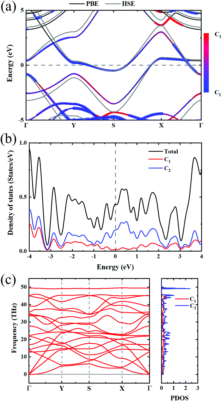 | ||
| Fig. 3 (a) Band structure of biphenylene. Black and gray lines represent PBE and HSE06 results, respectively. Color bar indicates the atomic contributions from the two types of carbon atoms circled in Fig. 1(a). (b) Density of states of biphenylene, where blue and red represent atomic contributions from carbon types shown in Fig. 1(a). (c) Phonon dispersion relation and phonon density of states. Red and blue colors in PDOS express the contributions from two types of carbon atoms in 2D biphenylene. | ||
Experimental research determined that nanoribbons, rather than infinite 2D materials, were much more likely to be synthesized. Thus, the properties of biphenylene nanoribbons are of vital importance. In this work, different widths of 6-ABNR up to 21-ABNR were modeled and investigated. In general, the band gaps of nanoribbons shrink as the corresponding width becomes larger, as presented in Fig. 4, where pink and green bars represent band gap calculations by the pure PBE and hybrid HSE06 functionals. It can be observed that when the width of nanoribbons is equal to or smaller than 12-ABNR, semiconductor behavior is exhibited. For nanoribbons wider than N = 15, in contrast, metallic properties similar to 2D biphenylene emerged. The wider the nanoribbon, the narrower the band gap. The computed band gap values at the HSE06 level of 6-ABNR, 9-ABNR and 12-ABNR were 1.35, 0.85 and 0.26 eV, respectively. This semiconductor–metal transition can be attributed to the stronger electronic confinement in both x and z directions, which opened gaps for narrow nanoribbons. But the band gap calculated in our work was smaller than those from previous experimental and theoretical research. In experiments, 6-ABNR exhibited a large band gap close to 2.35 eV,21 which is larger than that of the calculated result (1.35 eV). Compared to previous computational results at the HSE/6-31g** level reported by Hudspeth et al.38 and Fan and co-workers21 with atomic orbital based all-electron method, our band gap of 6-ABNR is smaller than those reported (1.71 eV and 1.81 eV). This can be ascribed to different methods employed in the calculations, in which the plane-wave pseudopotential technique was adopted in our study, while the all-electron atomic orbital-based scheme was used in previous studies.21,38 Note that both theoretical results underestimate band gaps for ABNRs when compared with experiments. This is a well-known deficiency of the DFT method.39,40 However, the overall trend of the closing of the band gap as the width of ABNR increase was accurately identified. The energy band structure calculations at both PBE and HSE06 levels are shown in Fig. 5(a)–(c), where solid and dashed lines represent PBE and HSE06 results, respectively. The band structures of 15-ABNR to 21-ABNR are presented in the ESI† (Fig. S1). The different types of carbon atoms from 6-ABNR to 12-ABNR are labeled in Fig. 5(a)–(c) by Ci. The corresponding carbon atoms from left to right are marked by colored circles in Fig. 5(d)–(f). One interesting feature noted was that, for 6-ABNR, both valence band maximum (VBM) and conduction band minimum (CBM) were located at the Γ point in the Brillouin zone, making it a direct band gap semiconductor. For 9-ABNR and 12-ABNR, however, CBM was located at the Γ point and VBM was located at the Y point, resulting in indirect behaviors. In order to investigate the electronic behavior of semiconductor nanoribbons near the band edge, the band structures projected on carbon atoms and electron distribution at VBM and CBM are given in Fig. 5(d)–(f), where red and green represent VBM and CBM, respectively. For 6-ABNR (Fig. 5(d)), the electronic density of VBM and CBM behave differently. The electronic density of VBM is mainly localized on two halves of the hex-ring, and a clear node of electronic density can be observed between the upper and lower regions. In contrast, the electronic density of CBM is localized at the carbon atoms pairs along the periodic direction of 6-ABNR. For 9-ABNR, a similar electronic density of CBM can be observed (Fig. 5(e)); however, the distribution of VBM, whose electronic density was mainly localized at the tetra-ring, is different from that of 6-ABNR. In addition, the partial charge at CB1, which is localized at the same k-point as the VBM, was also given in Fig. 5(f). Similar to the VBM, it was localized at carbon atoms that link two side-by-side hex rings. As mentioned in the analysis of the COHP of bonding of biphenylene, this side–side coupling is much weaker than the other couplings in biphenylene and may result in the shrinking of the direct band gap at the Y point. Thus, unlike 6-ABNR, 9-ABNR had an overall indirect band gap from Y to Γ. The case of 12-ABNR is similar to 9-ABNR (Fig. 5(d)). The CBM at Γ point has an electronic density similar to 6-ABNR and 9-ABNR, while the electronic density of VBM and CB1 are mainly located at the tetra-ring, and this weak side–side coupling shrinks the band gap at the Y point. In summary, the weak coupling of tetra-rings shrinks the band gap at the Y point and induces the direct–indirect transition of ABNR when the width increases.
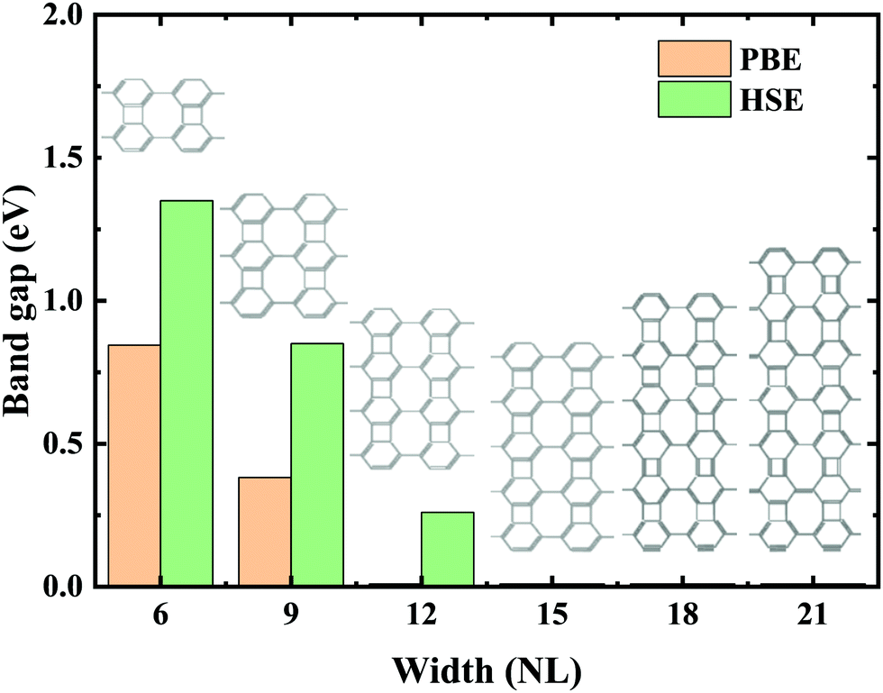 | ||
| Fig. 4 Variation of the band gap energy at various widths (the number of dimer lines, denoted as NL) for N-ABNR calculated by PBE (pink bars) and HSE06 level (green bars). | ||
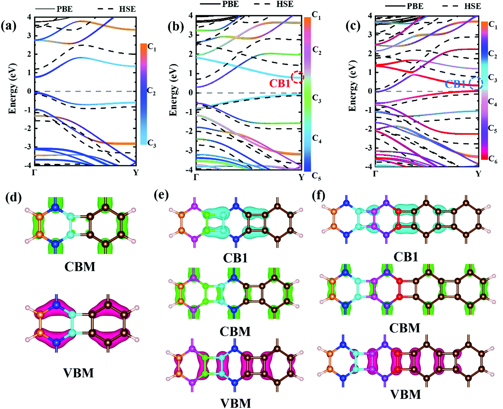 | ||
| Fig. 5 Band structures of nanoribbons with finite widths of (a) 6-ABNR, (b) 9-ABNR, and (c) 12-ABNR. The PBE and HSE06 band structures are represented by solid and dashed lines, respectively. The electronic distribution at the VBM and CBM for 6-ABNR to 12-ABNR are shown in (d)–(f), where red, green and cyan represent VBM, CBM and CB1, respectively. Different colors of atoms in (d)–(f) represent different types of carbon atoms, corresponding to color bars shown in (a)–(c). | ||
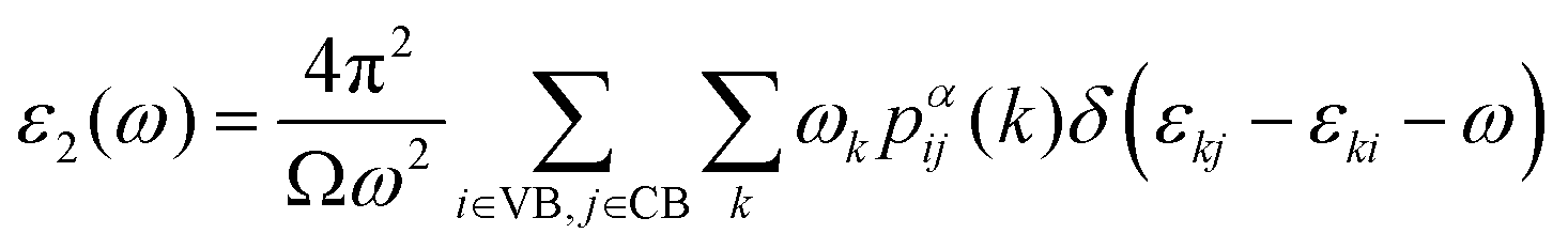
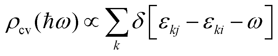
In addition to electronic properties, the optical properties of semiconductors are vital for potential applications and as indicated by the band structure calculations mentioned above, 6-ABNR, 9-ABNR and 12-ABNR behave like semiconductors. In order to study the optical properties of such nanoribbons, frequency-dependent dielectric functions were calculated at the HSE06 level. The imaginary part of the dielectric function α direction is given as a function of the photon energy ℏω expressed as
 | (1) |
 .
.
The contribution to the dielectric function is determined by the joint density of states and the matrix elements for the corresponding valence and conduction band. Because there are finite values for both near the Van Hove singularities as well as the matrix elements between the corresponding valence and conduction band, corresponding peaks appear in the dielectric function spectrum. Thus, using eqn (1), the matrix elements and the dielectric function can be calculated, and the band structures, the square of the transition dipole moment, and the dielectric function spectrum for 6-, 9- and 12-ABNR are shown in Fig. 6–8. In general, when the width of the ABNR is very narrow, the first peak of ε2 is located in a relatively high energy region due to the occurrence of a strong quantum confinement effect along the non-periodic direction and the peak red shift as such width expands.
 | ||
| Fig. 6 (a) Band structure scheme calculated for 6-ABNR. The black and red arrows indicate transitions occurring between subbands. (b) The x and y components of the square of transition dipole moment of 6-ABNR. (c and d) The frequency-dependent dielectric functions ε1(real) and ε2(imaginary) for 6-ABNR in the x and y directions, respectively. | ||
 | ||
| Fig. 7 (a) Band structure scheme calculated for 9-ABNR. The black and red arrows indicate transitions occurring between subbands. (b) The x and y components of the square of transition dipole moment of 9-ABNR. (c and d) The frequency-dependent dielectric functions ε1(real) and ε2(imaginary) for 9-ABNR in the x and y directions, respectively. | ||
 | ||
| Fig. 8 (a) Band structure scheme calculated for 12-ABNR. The black and red arrows indicate transitions occurring between subbands. (b) The x and y components of the square of transition dipole moment of 12-ABNR. (c and d) The frequency-dependent dielectric functions ε1(real) and ε2(imaginary) of 12-ABNR in the x and y directions, respectively. | ||
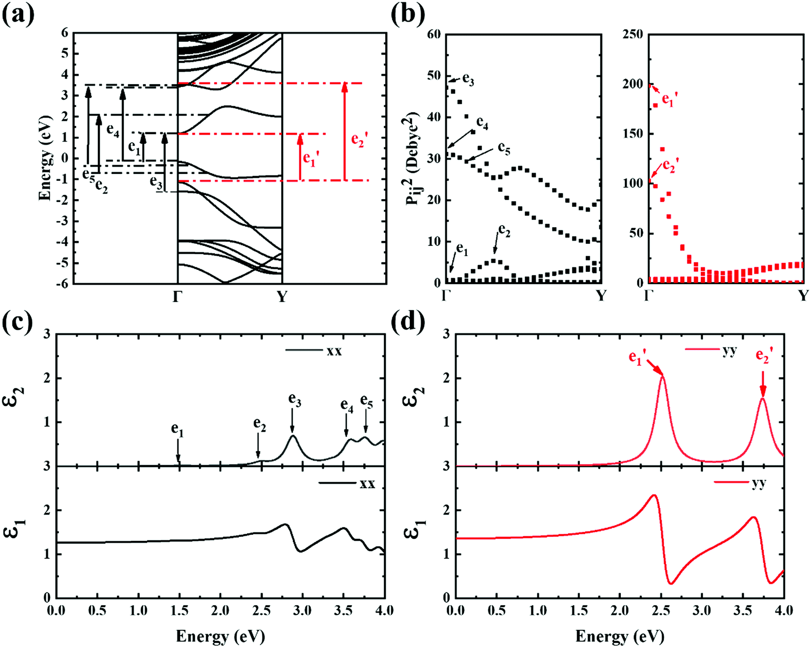
A strong anisotropic effect can be observed for the 6-ABNR (Fig. 6), 9-ABNR (Fig. 7) and 12-ABNR (Fig. 8) due to their finite size in the x direction. A red shift in the absorption edge was observed with the increase in the nanoribbon width, as predicted by the band gap (Fig. S2, ESI†). The optical band gaps were indicated by the first peak in the absorption spectrum. For 6-ABNR, the optical band gap is 2.52 eV, whereas it decreases to 1.32 eV for 9-ABNR and 1.09 eV for 12-ABNR.
In order to further investigate the optical properties, the imaginary part of the frequency dependent dielectric function ε2 and corresponding transition dipole moment were calculated. Fig. 6 shows the band structure, the square of the transition dipole moment and the ε2 spectrum for 6-ABNR (Fig. 6(b)). The corresponding optical transition is indicated schematically. It can be observed in the figure that the ε2 in the x direction consists of several peaks, the first four of which are located at 1.41, 2.48, 2.87, 3.58 and 3.75 eV. The dipole moment transitions between the six bands above and below Fermi-level. The transitions between two subbands μ and μ′,  , are designated as Eμμ′. The points e1, e3, and e4 were due to contributions of E11, E31 and E12 transitions at the Γ point, while e2 and e5 were due to contributions of E11 and E12 at k = 0.328π/a and k = 0.132π/a respectively. As for ε2 in the y direction, the two peaks had energies of 2.51 and 3.73 eV, indicated by e1′ and e2′ in Fig. 6(d). The transition dipole moment showed a maximum at the Γ point. These two transitions were due to contributions from E21 and E23 at the Γ point.
Next, the ε2 spectrum of 9-ABNR and its transition characteristics was explored (Fig. 7). The first six peaks of the ε2 spectrum at 1.59, 1.73, 2.29, 2.88, 3.21 and 3.54 eV in the x direction (Fig. 7(c)) were investigated. The transition dipole moment between subbands reached a maximum at Van Hove singular points, as shown in Fig. 7(b). Because the transition dipole moment in the x direction increased when compared to 6-ABNR, a larger magnitude of the ε2 spectrum was exhibited (Fig. 7(c)). While the transition dipole moment in the y direction was not altered significantly, the e1 and e5 peaks were contributed by E21 and E12 at the Γ point while e4 was a product of E12 at the Y point. On the other hand, e2, e3 and e6 were linked to E11, E11 and E13 where band crossing occurs near k = 0.14π/a, 0.4π/a and 0.14π/a, respectively. As for ε2 in the y direction, the five peaks correspond to 1.30, 1.59, 2.69, 3.23 and 3.87 eV. The transitions occurred at either the Γ or the Y point. The e1, e3, e4 and e5 correspond to E11, E41, E22 and E32 transitions at the Γ point, and e2 corresponds to E11 at the Y point.
Next, the transition properties of 12-ABNR are presented in Fig. 8. The transition dipole moment in the x direction further increases, as shown in Fig. 8(c). The peaks in the ε2 spectrum in the x direction are located at 1.06, 1.49, 2.57, 2.76, 3.14 and 3.62 eV (Fig. 8(c)). As illustrated in Fig. 8(b), these transitions were mainly located at the Γ point, with the exception being the e5 transition. While e1, e2, e3, e4 and e6 were contributed by E11, E31, E12, E13 and E34 at the Γ point, e5 was contributed by E22 at the Y point. As for ε2 in the y direction, the five peaks correspond to 1.48, 1.95, 2.61, 3.31 and 3.77 eV. The transitions occur at either the Γ or the Y point. The points e1, e3 and e5 correspond to contributions from E31, E51 and E42 transitions at the Γ point and e2 and e4 were contributed by E12 and E31, respectively, at the Y point.
In summary, by discussing optical properties together with band structures, the absorption edge red-shifted when the width of the ABNR increased. Strong anisotropy absorption can be observed for all ABNRs. By calculating the transition dipole moment for these ABNRs, the contribution of interband transitions to the dielectric function in 6-, 9-, and 12-armchair biphenylene nanoribbons (ABNRs) was identified. The lowest peaks in the imaginary part of the dielectric function ε2 spectrum were mainly contributed by Γ–Γ transitions.
4. Conclusions
In summary, first-principles calculations were employed to investigate the physical properties of biphenylene and its nanoribbon derivatives. The 2D pristine biphenylene sheet exhibited metallic properties. For 1D nanoribbons, because of their strong confinement effect, their band gaps shrink as the corresponding width increases. When the width reaches 15-ABNR, a semiconductor–metal phase transition occurs due to the weak coupling between carbon atoms in the tetra-rings. In addition, by examining the ε2 spectrum and corresponding transition dipole moments, the contributions of transitions in 6-, 9-, 12-ABNR can be identified. The lowest peaks in the ε2 spectrum were mainly due to contributions from Γ–Γ transitions. As the width of the ABNR increases, transitions in the x direction become stronger while the transition strength in the y direction is not significantly altered.Conflicts of interest
There are no conflicts to declare.Acknowledgements
Work at the Fudan University was supported by the key projects of basic research of Shanghai Municipal Science and Technology Commission (No. 18JC1411500) and the National Natural Science Foundation of China (Grant No. 11374055 and 61427815). W.-S. Su would like to thank the Ministry of Science and Technology of Taiwan for financially supporting this research under Contract No. MOST-110-2112-M-979-001. Support from the National Centers for Theoretical Sciences and High-performance Computing of Taiwan in providing significant computing resources to facilitate this research are also gratefully acknowledged.References
- S. Zhang, J. Zhou, Q. Wang, X. Chen, Y. Kawazoe and P. Jena, Proc. Natl. Acad. Sci. U. S. A., 2015, 112, 2372 CrossRef CAS PubMed.
- A. Gupta, T. Sakthivel and S. Seal, Prog. Mater. Sci., 2015, 73, 44–126 CrossRef CAS.
- S. Z. Butler, S. M. Hollen, L. Cao, Y. Cui, J. A. Gupta, H. R. Gutiérrez, T. F. Heinz, S. S. Hong, J. Huang, A. F. Ismach, E. Johnston-Halperin, M. Kuno, V. V. Plashnitsa, R. D. Robinson, R. S. Ruoff, S. Salahuddin, J. Shan, L. Shi, M. G. Spencer, M. Terrones, W. Windl and J. E. Goldberger, ACS Nano, 2013, 7, 2898–2926 CrossRef CAS PubMed.
- M. J. Allen, V. C. Tung and R. B. Kaner, Chem. Rev., 2010, 110, 132–145 CrossRef CAS PubMed.
- R. Mas-Ballesté, C. Gómez-Navarro, J. Gómez-Herrero and F. Zamora, Nanoscale, 2011, 3, 20–30 RSC.
- Y. Lin and J. W. Connell, Nanoscale, 2012, 4, 6908–6939 RSC.
- S. M. Loh, Y.-H. Huang, K.-M. Lin, W. S. Su, B. R. Wu and T. C. Leung, Phys. Rev. B: Condens. Matter Mater. Phys., 2014, 90, 035450 CrossRef CAS.
- S. R. Das, J. Kwon, A. Prakash, C. J. Delker, S. Das and D. B. Janes, Appl. Phys. Lett., 2015, 106, 083507 CrossRef.
- N. Huo, J. Kang, Z. Wei, S.-S. Li, J. Li and S.-H. Wei, Adv. Funct. Mater., 2014, 24, 7025–7031 CrossRef CAS.
- H. Wang, X. Yuan, G. Zeng, Y. Wu, Y. Liu, Q. Jiang and S. Gu, Adv. Colloid Interface Sci., 2015, 221, 41–59 CrossRef CAS PubMed.
- F. Schwierz, Nat. Nanotechnol., 2010, 5, 487–496 CrossRef CAS PubMed.
- A. C. Ferrari, F. Bonaccorso, V. Fal'ko, K. S. Novoselov, S. Roche, P. Bøggild, S. Borini, F. H. L. Koppens, V. Palermo, N. Pugno, J. A. Garrido, R. Sordan, A. Bianco, L. Ballerini, M. Prato, E. Lidorikis, J. Kivioja, C. Marinelli, T. Ryhänen, A. Morpurgo, J. N. Coleman, V. Nicolosi, L. Colombo, A. Fert, M. Garcia-Hernandez, A. Bachtold, G. F. Schneider, F. Guinea, C. Dekker, M. Barbone, Z. Sun, C. Galiotis, A. N. Grigorenko, G. Konstantatos, A. Kis, M. Katsnelson, L. Vandersypen, A. Loiseau, V. Morandi, D. Neumaier, E. Treossi, V. Pellegrini, M. Polini, A. Tredicucci, G. M. Williams, B. Hee Hong, J.-H. Ahn, J. Min Kim, H. Zirath, B. J. van Wees, H. van der Zant, L. Occhipinti, A. Di Matteo, I. A. Kinloch, T. Seyller, E. Quesnel, X. Feng, K. Teo, N. Rupesinghe, P. Hakonen, S. R. T. Neil, Q. Tannock, T. Löfwander and J. Kinaret, Nanoscale, 2015, 7, 4598–4810 RSC.
- Z. Wang, F. Dong, B. Shen, R. J. Zhang, Y. X. Zheng, L. Y. Chen, S. Y. Wang, C. Z. Wang, K. M. Ho, Y.-J. Fan, B.-Y. Jin and W.-S. Su, Carbon, 2016, 101, 77–85 CrossRef CAS.
- G. Brunetto, P. A. S. Autreto, L. D. Machado, B. I. Santos, R. P. B. dos Santos and D. S. Galvão, J. Phys. Chem. C, 2012, 116, 12810–12813 CrossRef CAS.
- M. De La Pierre, P. Karamanis, J. Baima, R. Orlando, C. Pouchan and R. Dovesi, J. Phys. Chem. C, 2013, 117, 2222–2229 CrossRef CAS.
- O. Rahaman, B. Mortazavi, A. Dianat, G. Cuniberti and T. Rabczuk, FlatChem, 2017, 1, 65–73 CrossRef CAS.
- Q. Song, B. Wang, K. Deng, X. Feng, M. Wagner, J. D. Gale, K. Müllen and L. Zhi, J. Mater. Chem. C, 2013, 1, 38–41 RSC.
- G. Li, Y. Li, H. Liu, Y. Guo, Y. Li and D. Zhu, Chem. Commun., 2010, 46, 3256–3258 RSC.
- Z. Li, Y. Xie, P.-Y. Chang and Y. Chen, Carbon, 2020, 157, 563–569 CrossRef CAS.
- Y. Cao, V. Fatemi, S. Fang, K. Watanabe, T. Taniguchi, E. Kaxiras and P. Jarillo-Herrero, Nature, 2018, 556, 43–50 CrossRef CAS PubMed.
- Q. Fan, L. Yan, M. W. Tripp, O. Krejčí, S. Dimosthenous, S. R. Kachel, M. Chen, A. S. Foster, U. Koert, P. Liljeroth and J. M. Gottfried, Science, 2021, 372, 852 CrossRef CAS PubMed.
- A. Bafekry, M. Faraji, M. M. Fadlallah, H. R. Jappor, S. Karbasizadeh, M. Ghergherehchi and D. Gogova, J. Phys.: Condens. Matter, 2022, 34, 015001 Search PubMed.
- Y. Liao, X. Shi, T. Ouyang, C. Zhang, J. Li, C. Tang, C. He and J. Zhong, arXiv e-prints, 2021, arXiv:2107.01436.
- G. Kresse and J. Furthmüller, Comput. Mater. Sci., 1996, 6, 15–50 CrossRef CAS.
- G. Kresse and J. Hafner, Phys. Rev. B: Condens. Matter Mater. Phys., 1994, 49, 14251–14269 CrossRef CAS PubMed.
- G. Kresse and D. Joubert, Phys. Rev. B: Condens. Matter Mater. Phys., 1999, 59, 1758–1775 CrossRef CAS.
- J. P. Perdew, K. Burke and M. Ernzerhof, Phys. Rev. Lett., 1996, 77, 3865–3868 CrossRef CAS PubMed.
- H. J. Monkhorst and J. D. Pack, Phys. Rev. B: Solid State, 1976, 13, 5188–5192 CrossRef.
- R. Dronskowski and P. E. Bloechl, J. Phys. Chem., 1993, 97, 8617–8624 CrossRef CAS.
- V. L. Deringer, A. L. Tchougréeff and R. Dronskowski, J. Phys. Chem. A, 2011, 115, 5461–5466 CrossRef CAS PubMed.
- A. Togo and I. Tanaka, Scr. Mater., 2015, 108, 1–5 CrossRef CAS.
- V. Wang, N. Xu, J.-C. Liu, G. Tang and W.-T. Geng, Comput. Phys. Commun., 2021, 267, 108033 CrossRef CAS.
- V. Wang, Y.-Y. Liang, Y. Kawazoe and W.-T. Geng, arXiv e-prints, 2018, arXiv:1806.04285.
- R. Wang, S. Wang, X. Wu and X. Liang, Phys. B, 2010, 405, 3501–3506 CrossRef CAS.
- F. Liu, P. Ming and J. Li, Phys. Rev. B: Condens. Matter Mater. Phys., 2007, 76, 064120 CrossRef.
- C. Lee, X. Wei, J. W. Kysar and J. Hone, Science, 2008, 321, 385–388 CrossRef CAS PubMed.
- M. Diem, Modern Vibrational Spectroscopy and Micro-Spectroscopy: Theory, Instrumentation and Biomedical Applications, John Wiley & Sons, Inc: Chichester, West Sussex, 2015, pp. 397–398 Search PubMed.
- M. A. Hudspeth, B. W. Whitman, V. Barone and J. E. Peralta, ACS Nano, 2010, 4, 4565–4570 CrossRef CAS PubMed.
- J. P. Perdew, Int. J. Quantum Chem., 1985, 28, 497–523 CrossRef.
- L. Yang, C.-H. Park, Y.-W. Son, M. L. Cohen and S. G. Louie, Phys. Rev. Lett., 2007, 99, 186801 CrossRef PubMed.
- T. H. Cho, W. S. Su, T. C. Leung, W. Ren and C. T. Chan, Phys. Rev. B: Condens. Matter Mater. Phys., 2009, 79, 235123 CrossRef.
Footnote |
| † Electronic supplementary information (ESI) available. See DOI: 10.1039/d1cp04481h |
| This journal is © the Owner Societies 2022 |