
 Open Access Article
 This Open Access Article is licensed under a Creative Commons Attribution-Non Commercial 3.0 Unported Licence
Low thermal conductivity in franckeite heterostructures†
Jean
Spiece‡
 a,
Sara
Sangtarash
b,
Marta
Mucientes
a,
Aday J.
Molina-Mendoza
c,
Kunal
Lulla§
a,
Thomas
Mueller
c,
Oleg
Kolosov
*a,
Hatef
Sadeghi
*b and
Charalambos
Evangeli¶
*a
a,
Sara
Sangtarash
b,
Marta
Mucientes
a,
Aday J.
Molina-Mendoza
c,
Kunal
Lulla§
a,
Thomas
Mueller
c,
Oleg
Kolosov
*a,
Hatef
Sadeghi
*b and
Charalambos
Evangeli¶
*a
aPhysics Department, Lancaster University, Lancaster LA1 4YW, UK. E-mail: o.kolosov@lancaster.ac.uk; ch.evangeli@gmail.com
bDevice Modelling Group, School of Engineering, University of Warwick, CV4 7AL Coventry, UK. E-mail: Hatef.Sadeghi@warwick.ac.uk
cVienna University of Technology, Gusshausstrasse 27-29, Vienna A-1040, Austria
First published on 27th January 2022
Abstract
Layered crystals are known to be good candidates for bulk thermoelectric applications as they open new ways to realise highly efficient devices. Two dimensional materials, isolated from layered materials, and their stacking into heterostructures have attracted intense research attention for nanoscale applications due to their high Seebeck coefficient and possibilities to engineer their thermoelectric properties. However, integration to thermoelectric devices is problematic due to their usually high thermal conductivities. Reporting on thermal transport studies between 150 and 300 K, we show that franckeite, a naturally occurring 2D heterostructure, exhibits a very low thermal conductivity which combined with its previously reported high Seebeck coefficient and electrical conductance make it a promising candidate for low dimensional thermoelectric applications. We find cross- and in-plane thermal conductivity values at room temperature of 0.70 and 0.88 W m−1 K−1, respectively, which is one of the lowest values reported today for 2D-materials. Interestingly, a 1.77 nm thick layer of franckeite shows very low thermal conductivity similar to one of the most widely used thermoelectric material Bi2Te3 with the thickness of 10–20 nm. We show that this is due to the low Debye frequency of franckeite and scattering of phonon transport through van der Waals interface between different layers. This observation open new routes for high efficient ultra-thin thermoelectric applications.
Thermoelectric materials are of great interest due to their ability to fabricate devices which convert the waste heat into electricity. Efficient thermoelectric devices require tuning of the materials Seebeck coefficient, electrical and thermal conductivity.1 The efficiency of a thermoelectric material is given by the thermoelectric figure of merit, ZT = (σS2T)/k, and it is proportional to the square of the Seebeck coefficient S and electrical conductivity σ and inversely proportional to the thermal conductivity k.2 Therefore, materials combining high S and σ and low k, which are generally rare, are ideal candidates for such devices. Many strategies have been applied to decrease the k without affecting the σ including creation of structural disorders, synthesize materials with complex crystal structures, and use of organic-hybrid materials or low-dimensional nano-structured materials.3
Layered crystals are known to be good candidates for integration in thermoelectric applications,4 such as the Bi2Te3-alloys which are among the best performing thermoelectric materials. Exfoliating such crystals, resulting in two dimensional (2D) materials, provide great opportunities to challenge commercially used materials as they offer the unique possibility of engineering their thermal conductivity.5–7 By stacking different 2D-materials to create van der Waals (vdW) heterostructures, the phonon mismatch between the layers can be controlled and with the right assembly the thermal conductivity is reduced. Strategies like stacking Bi2Te3 exfoliated thin films to form ‘pseudosuperlattice’,8,9 stacking graphene and MoS2 monolayers10,11 or inserting different intercalants such as SnS and BiS into TiS2 vdW gap and creation of superlattices12,13 have been successful to decrease the thermal conductivity.
Instead of attempting the often very demanding 2D-materials stacking, another strategy consists in using nature's ability of creating heterostructures. In contrast to a fabricated 2D-heterostructure, a natural one do not have any issues such as alignment or trapped residues in between the layers, which might cause uncontrolled change of the thermal or electrical resistance. Franckeite is such a material consisting of stacks of SnS2 – like pseudohexagonal (H) and PbS – like pseudotetragonal (Q) layers (see Fig. 1a) which can be isolated by liquid or air exfoliation.14,15 It demonstrates high electrical conductance with a narrow bandgap of 0.5–0.7 eV and a Seebeck coefficient of 264 μV K−1 at room temperature15 which makes it an attractive candidate for realization of novel thermoelectric devices.
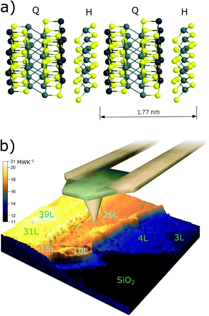 | ||
| Fig. 1 (a) Crystal structure of Frankeite. (b) Schematic representation of the SThM measurement, with 3D thermal resistance image at Ts = 156 K. Number of layers for the different areas are shown on the image (scan dimensions 5 × 5 m). | ||
Here, we show that franckeite poses a very low thermal conductivity, which in combination with the high Seebeck coefficient and electrical conductance reported in the literature experimentally and calculated below, make franckeite a very promising candidate for thermoelectric applications. We study the thermal transport properties of thin flakes at various temperatures starting from 150 K up to room temperature with Scanning Thermal Microscopy (SThM). We show that Franckeite H + Q layer has a very low in-plane and cross-plane thermal conductivity compared to other exfoliated or ultra-thin-film materials. This is supported by our Density Functional Theory (DFT) calculations which reveals that Franckeite has a low Debye frequency and therefore has low thermal conductivity.
Fig. 1a shows the molecular structure of layered franckeite. Our calculation using first principle simulations shows that the Debye frequency of franckeite is about ħω = 40 meV. This means that franckeite is a soft material as confirmed by our Ultrasonic Force Microscopy study (see ESI note 2†) and can potentially possess a low thermal conductivity. Motivated by this observation, we isolated franckeite flakes on 280 nm SiO2 on Si by mechanical exfoliation (see ESI note 5†), resulting in areas of various thicknesses. We thermally characterise the sample by means of high vacuum SThM16 at sample temperatures, Ts, varying from 150 K–300 K as described elsewhere.10 Briefly, at each sample temperature, we thermally image the sample and record approach-retract SThM cycles. The tip–sample thermal contact resistance, RX, for each pixel of the thermal image is obtained from the in-contact SThM image, the out-of-contact SThM signal of the approach-retract curve, and the electrical resistance to temperature SThM probe calibration.17Fig. 1b shows a 3D representation of the thermal resistance image acquired at Ts = 156 K. Areas with thicknesses varying from 5 to 66 nm can be identified from the topography image (see ESI note 1†). Considering a H + Q layer thickness of about 1.77 nm,15 we can identify areas consisting of 3, 4, 10, 26, 31, 39 of H + Q layers. The flakes’ thermal resistance is higher than the one of Si/SiO2 substrate and increases with the thickness.
We extracted the average mean thermal resistance for each area and plotted it as a function of thickness at various temperatures (see Fig. 2a). Note, that small local variations in RX due to some wrinkles formed by the exfoliation process, are reflected in the error bars of the average thermal conductance for each area. Furthermore, due to the high resistance of the material itself, the atomic structure of the top layer (H or Q), is not expected to significantly affect the average RX of the different areas. RX increases with a high rate for the first 10 layers and then almost saturates, implying that after a certain thickness, we are probing the thermal resistance of bulk franckeite. The increasing resistance with thickness trend is expected for layers with lower or comparable to the substrate thermal conductivity, because they act as extra resistive interfaces for the heat flow to the substrate heat sink. For highly thermally conductive layers, such as graphene, the trend is opposite18,19 because they act as extra heat transfer channels. The thermal resistance evolution with thickness could be a purely thickness dependent effect, related with thermal conductivity variation or substrate effect. In general the thermal conductivity of 2D-materials is also affected when they are placed on a substrate due to change in the phonon dispersion and increase of the phonon scattering rate.18,20,21
 | ||
| Fig. 2 (a) Thermal resistance RX as a function of temperature for areas of different thicknesses (b) In-plane ki and cross-plain kc thermal conductivity of franckeite H + Q flake of 1.77 nm thickness. | ||
Regarding the temperature dependence, RX for all thicknesses decreases with temperature, with the higher rate being for the thicker areas. For thinner areas (less than 10 layers), RX is dominated by the thermal resistance of SiO2 as revealed by the similar to SiO2 thermal resistance (RX–S) trend with temperature (see also ESI note 1†). In contrast, for thicker areas, RX decreases in a different manner than RX–S. The RX saturation with temperature for thicker franckeite (more than 10 layers) is different than the SiO2 trend. This observation implies that for such thicknesses, SThM is more sensitive to the material rather than the substrate properties.
To quantify the thermal conductivity of a single franckeite H + Q layer we assume diffusive thermal transport and thickness independent thermal conductivity. Franckeite, in contrast to other 2D-materials, has a complex structure consisting of heavy atoms which is likely leading to a diffusive thermal transport mechanism.22 For such structures of low thermal conductivity it is not evident that thermal conductivity is strongly influenced by the number of layers.20 Under these assumptions we express the thermal SThM measured resistance as a sum of resistances: RX = Rt + Rint + Rs, where Rt is the SThM tip thermal resistance, Rint the tip-franckeite thermal boundary resistance and Rs is the sample spreading resistance. Rt and Rint are not thickness-dependent and they remain constant for the different sample areas. With the use of a diffusive thermal transport model for layered material on a substrate, we express Rs as a function of the layer thickness and the thermal conductivities of the substrate and the material.19,23–26 By fitting the data for each temperature we extract the cross-plane (kc) and in-plane (ki) thermal conductivity (see Experimental section and ESI note 3† for more details on the modelling, fitting procedure and accuracy).
In Fig. 2b, kc and ki are plotted for each temperature. Both kc and ki are found to increase with temperature from 0.28 and 0.44 W m−1 K−1 at 156 K to 0.70 and 0.88 W m−1 K−1 at room temperature, respectively. The thermal conductivity increase rate is much higher for temperatures higher than 240 K, and for temperatures higher than 275 K it tends to saturate. The anisotropy has a small decrease with temperature, which is possibly related with the activation of some phonon modes with temperature (see also ESI note 4†).
In most solids, at very low temperatures, the phonon mean free path is relatively independent of temperature and thermal conductance increases with temperature until the Debye temperature of the material is reached. Afterward, the thermal conductance increases slightly with temperature. For higher temperatures, due to strong lattice vibrations shortening the phonon mean free path, the conductivity decreases with temperature.27 This behaviour has been reported in different 2D-materials.28 For franckeite, one would expect saturation of thermal conductivity at relatively low temperatures and slight increase afterward due to its low Debye frequency as shown in our kp calculations in Fig. 3a. However, we observe a sharp increase of the thermal conductivity around 250 K. This behaviour could be related to different mechanisms. First, such behaviour could be the signature of a possible amorphous-crystalline transition. In the case of franckeite, this is very unlikely as franckeite is a crystalline material15,29 and no amorphous phase has been reported in our temperature range. Secondly, we cannot exclude the presence of polymers residues, due to the exfoliation process. Such contamination was shown to affects phonon transport of 2D-materials and becomes more important as temperature is decreased.30
 | ||
| Fig. 3 (a) Phonon band-structure of franckeite with the lattice structure shown in Fig. 1b. (b) Number of open phonon conduction channel and (c) electron and phonon contribution to thermal conductivity. | ||
To understand the physical mechanisms behind the thermal conductivity values and trends, we calculate the phonon band structure of franckeite (see Fig. 3a) using density functional theory (see ESI note 4†). From the band structure, we calculate the number of open phonon conduction channels in franckeite (Fig. 3b) and its intrinsic thermal conductivity (Fig. 3c). Our calculation shows that there are multiple open phonon channels between 0–16 meV and 20–36 meV but there are very few between 16–20 meV due to a gap in phonon band structure. This gap and relatively low Debye frequency of franckeite leads to a calculated cross-plane thermal conductivity of ∼1.2 W m−1 K−1 at room temperature. This is the intrinsic thermal conductivity of franckeite (upper bound thermal conductivity) because in the calculations, we do not take scattering at the interfaces between electrodes and franckeite layers into account.
In order to calculate Seebeck coefficient and electron contribution to thermal conductance, we perform DFT calculations combined with quantum transport to obtain the number of open conduction channels through franckeite heterostructure. Fig. 4a shows the number of open conduction channels due to electrons. We then use this to calculate Seebeck coefficient in franckeite (see ESI note 4†). Fig. 4b shows the Seebeck coefficient versus different Fermi energy of electrodes at room temperature. Around DFT Fermi energy, the calculated Seebeck coefficient approaches values 280 μV K−1 that is in very good agreement with the measured values31 and is similar to the ones of high ZT-value thermoelectric materials for room temperature applications. For example, Bi2Te3 synthesized by alloying with Sb, has Seebeck coefficient of 242 μ VK−1 with ZT = 1.8632 while MgAgSb-based TE materials 285 μ VK−1 with ZT = 1.1.33 Since the thermal conductance in franckeite is smaller than these materials, a higher ZT is expected in franckeite. At DFT Fermi energy, the contribution from electrons to thermal conductance is about 0.1 W m−1 K−1 which is about 10% of phonon contributions to thermal conductance (Fig. 4c).
 | ||
| Fig. 4 Electron transport through franckeite. (a) Number of open conduction channels due to electrons calculated using DFT. (b) Calculated Seebeck coefficient at room temperature versus Fermi energy of electrodes. (c) Electron contribution to thermal conductance at room temperature versus Fermi energy of electrodes. | ||
The kc and ki values at room temperature, to the best of our knowledge, are the lowest values reported up to date for materials with similar thickness including mono- or few-layers of exfoliated materials or ultra-thin films suitable for thermoelectric applications. Fig. 5 shows thermal conductivity values of typical layered thermoelectric materials with thickness in addition to some bulk-materials values. An H + Q franckeite layer has the lowest in-plane and cross-plane thermal conductivities compared to all other materials with similar thickness. Interestingly, the thermal conductivity of a 1.77 nm thick H + Q franckeite is similar to that reported for Bi2Te3 nanoplates but with a thickness of 10–20 nm as measured34 or calculated theoretically.9
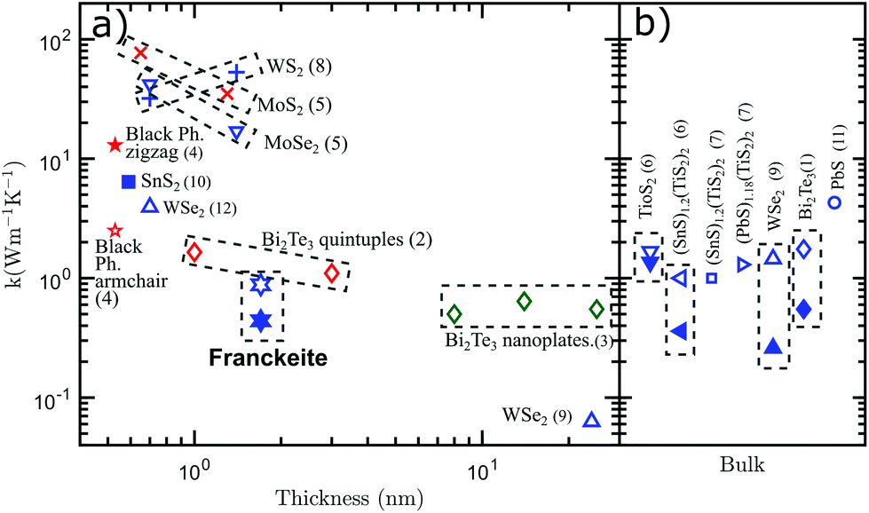 | ||
| Fig. 5 (a and b) Reported thermal conductivity values of layered materials with thickness (a) and of bulk layered materials (b). Note that, at (b) when two values for the same material are shown they correspond to cross- (filled) and in- (non-filled) plane values. The data comes from: (1),8 (2),9 (3),34 (4),35 (5),36 (6),12 (7),13 (8),37 (9),38 (10),39 (11),40 (12).41 | ||
Thermal conductivity of a H + Q franckeite is two orders of magnitude lower than WS2![[thin space (1/6-em)]](https://www.rsc.org/images/entities/char_2009.gif) 37 with this ratio even larger for MoS236 which is having very high Seebeck coefficient however, being unsuitable for thermoelectrics due to its high thermal conductivity. It is almost an order of magnitude lower than black phosphorous35 which has similar Seebeck coefficient as franckeite. It is just one order of magnitude higher than WSe2,38 which is the lowest thermal conductivity continuous material, but it is lower than its monolayer.41 Furthermore, franckeite's thermal conductivity is smaller than most bulk layered materials with inserteddifferent intercalants in the vdW gap designed for thermoelectric applications such as (SnS)1.2 (TiS2)2, (PbS)1.18 (TiS2)2, (BiS)1.2 (TiS2)2 and (SnS)1.2 (TiS2)2. The interacalation method has as a result the creation of superlattices and the decrease of the thermal conductivity of the initial material due to suppressed phonon transport caused by weaker interlayer bonding.12 In the case of franckeite which has a natural superlattice is interesting to see the relation between the H + Q layers thermal conductivity and H layer itself. The thermal conductivity of SnS2 layer39 (H layer of franckeite), is almost an order of magnitude higher than the H + Q layers together. This is because of the additional phonon scattering at the interface42 between H and Q layers and through Q layer as demonstrated using a tight-binding model in the ESI note 4.†
37 with this ratio even larger for MoS236 which is having very high Seebeck coefficient however, being unsuitable for thermoelectrics due to its high thermal conductivity. It is almost an order of magnitude lower than black phosphorous35 which has similar Seebeck coefficient as franckeite. It is just one order of magnitude higher than WSe2,38 which is the lowest thermal conductivity continuous material, but it is lower than its monolayer.41 Furthermore, franckeite's thermal conductivity is smaller than most bulk layered materials with inserteddifferent intercalants in the vdW gap designed for thermoelectric applications such as (SnS)1.2 (TiS2)2, (PbS)1.18 (TiS2)2, (BiS)1.2 (TiS2)2 and (SnS)1.2 (TiS2)2. The interacalation method has as a result the creation of superlattices and the decrease of the thermal conductivity of the initial material due to suppressed phonon transport caused by weaker interlayer bonding.12 In the case of franckeite which has a natural superlattice is interesting to see the relation between the H + Q layers thermal conductivity and H layer itself. The thermal conductivity of SnS2 layer39 (H layer of franckeite), is almost an order of magnitude higher than the H + Q layers together. This is because of the additional phonon scattering at the interface42 between H and Q layers and through Q layer as demonstrated using a tight-binding model in the ESI note 4.†
In summary, with a combined experimental and theoretical study the thermal properties of franckeite natural heterostructure in the nano-scale, for temperatures ranging from 150 to 300 K were studied. In-plane and cross-plane thermal conductivity range from 0.28 and 0.44 W m−1 K−1 at 156 K to 0.70 and 0.88 W m−1 K−1, respectively at room temperature. We showed that the low thermal conductivity values are due to the a gap in phonon band structure, the low Debye frequency and the additional phonon scattering at the interface between H and Q layers of franckeite. These values which are among the lowest reported for 2D-materials and ultra-thin-films, that in combination to the high electrical conductivity and Seebeck coefficient make franckeite a promising candidate for integration to micro-scale thermoelectric applications at room temperature.
Author contributions
Jean Spiece: Writing – original draft, conceptualization, methodology, validation, formal analysis, investigation. Sara Sangtarash: Writing – review & editing, methodology, validation. Marta Mucientes: Investigation, writing – review & editing. Aday J. Molina-Mendoza: Investigation, writing – review & editing. Kunal Lulla: Investigation. Thomas Mueller: Funding acquisition, resources. Oleg Kolosov: Funding acquisition, writing – review & editing, methodology, resources, conceptualization. Hatef Sadeghi: Funding acquisition, writing – original draft, methodology, resources, conceptualization, supervision. Charalambos Evangeli: Writing – original draft, conceptualization, methodology, validation, formal analysis, investigation, supervision.Conflicts of interest
There are no conflicts to declare.Acknowledgements
H. S. acknowledges the UKRI for Future Leaders Fellowship number MR/S015329/2. S. S acknowledges the Leverhulme Trust for Early Career Fellowship no. ECF-2018-375. O. K., C. E., and J. S. acknowledge the support of the EU grant QUANTIHEAT (project # 604668). O. K. acknowledges core 3 Graphene Flagship EU project and EP/v00767XII EPSRC grant. A. J. M.-M. acknowledges financial support from the European Commission (Marie Sklodowska-Curie Individual Fellowships, OPTOvanderWAALS, grant ID 791536).References
- J. R. Sootsman, D. Y. Chung and M. G. Kanatzidis, Angew. Chem., Int. Ed., 2009, 48, 8616–8639 CrossRef CAS PubMed.
- K. Biswas, J. He, I. D. Blum, C.-I. Wu, T. P. Hogan, D. N. Seidman, V. P. Dravid and M. G. Kanatzidis, Nature, 2012, 489, 414–418 CrossRef CAS PubMed.
- Y. Yin, K. Baskaran and A. Tiwari, Phys. Status Solidi A, 2019, 216, 1800904 CrossRef.
- M. Samanta, T. Ghosh, S. Chandra and K. Biswas, J. Mater. Chem. A, 2020, 8, 12226–12261 RSC.
- E. C. Ahn, H.-S. P. Wong and E. Pop, Nat. Rev. Mater., 2018, 3, 1–15 CrossRef.
- G. Ding, C. Wang, G. Gao, K. Yao, C. Dun, C. Feng, D. Li and G. Zhang, Nanoscale, 2018, 10, 7077–7084 RSC.
- Y. Hu, Y. Yin, G. Ding, J. Liu, H. Zhou, W. Feng, G. Zhang and D. Li, Mater. Today Phys., 2021, 17, 100346 CrossRef CAS.
- D. Teweldebrhan, V. Goyal and A. A. Balandin, Nano Lett., 2010, 10, 1209–1218 CrossRef CAS PubMed.
- B. Qiu and X. Ruan, Appl. Phys. Lett., 2010, 97, 183107 CrossRef.
- C. Evangeli, J. Spiece, S. Sangtarash, A. J. Molina-Mendoza, M. Mucientes, T. Mueller, C. Lambert, H. Sadeghi and O. Kolosov, Adv. Electron. Mater., 2019, 5, 1900331 CrossRef CAS.
- H. Sadeghi, S. Sangtarash and C. J. Lambert, 2D Mater., 2016, 4, 015012 CrossRef.
- C. Wan, Y. Wang, N. Wang, W. Norimatsu, M. Kusunoki and K. Koumoto, J. Electron. Mater., 2011, 40, 1271–1280 CrossRef CAS.
- C. Wan, Y. Wang, N. Wang and K. Koumoto, Materials, 2010, 3, 2606–2617 CrossRef CAS.
- M. Velickỳ, P. S. Toth, A. M. Rakowski, A. P. Rooney, A. Kozikov, C. R. Woods, A. Mishchenko, L. Fumagalli, J. Yin and V. Zólyomi, et al. , Nat. Commun., 2017, 8, 1–11 CrossRef PubMed.
- A. J. Molina-Mendoza, E. Giovanelli, W. S. Paz, M. A. Niño, J. O. Island, C. Evangeli, L. Aballe, M. Foerster, H. S. Van Der Zant and G. Rubio-Bollinger, et al. , Nat. Commun., 2017, 8, 1–9 CrossRef PubMed.
- S. Gomès, A. Assy and P.-O. Chapuis, Phys. Status Solidi A, 2015, 212, 477–494 CrossRef.
- J. Spiece, C. Evangeli, K. Lulla, A. Robson, B. Robinson and O. Kolosov, J. Appl. Phys., 2018, 124, 015101 CrossRef.
- M. E. Pumarol, M. C. Rosamond, P. Tovee, M. C. Petty, D. A. Zeze, V. Falko and O. V. Kolosov, Nano Lett., 2012, 12, 2906–2911 CrossRef CAS PubMed.
- F. Menges, H. Riel, A. Stemmer, C. Dimitrakopoulos and B. Gotsmann, Phys. Rev. Lett., 2013, 111, 205901 CrossRef PubMed.
- X. Gu, Y. Wei, X. Yin, B. Li and R. Yang, Rev. Mod. Phys., 2018, 90, 041002 CrossRef CAS.
- A. A. Balandin, Nat. Mater., 2011, 10, 569–581 CrossRef CAS PubMed.
- M. Shen and P. Keblinski, J. Appl. Phys., 2014, 115, 144310 CrossRef.
- M. M. Yovanovich, J. R. Culham and P. Teertstra, IEEE Trans. Compon., Packag., Manuf. Technol., Part A, 1998, 21, 168–176 CrossRef.
- G. Hwang and O. Kwon, Nanoscale, 2016, 8, 5280–5290 RSC.
- M. M. Sadeghi, S. Park, Y. Huang, D. Akinwande, Z. Yao, J. Murthy and L. Shi, J. Appl. Phys., 2016, 119, 235101 CrossRef.
- J. Spièce, C. Evangeli, A. J. Robson, A. El Sachat, L. Haenel, M. I. Alonso, M. Garriga, B. J. Robinson, M. Oehme and J. Schulze, et al. , Nanoscale, 2021, 13, 10829–10836 RSC.
- C. Kittel, P. McEuen and P. McEuen, Introduction to solid state physics, Wiley, New York, 1996, vol. 8 Search PubMed.
- Y. Wang, N. Xu, D. Li and J. Zhu, Adv. Funct. Mater., 2017, 27, 1604134 CrossRef.
- T. Williams and B. Hyde, Phys. Chem. Miner., 1988, 15, 521–544 CrossRef CAS.
- I. Jo, M. T. Pettes, J. Kim, K. Watanabe, T. Taniguchi, Z. Yao and L. Shi, Nano Lett., 2013, 13, 550–554 CrossRef CAS PubMed.
- A. Molina-Mendoza, E. Giovanelli, W. Paz, M. Angel Niño, J. Island, C. Evangeli, L. Aballe, M. Foerster, H. van der Zant, G. Rubio-Bollinger, N. Agraï, J. Palacios, E. Pérez and A. Castellanos-Gomez, Nat. Commun., 2017, 8, 14409 CrossRef CAS PubMed.
- X.-L. Shi, J. Zou and Z.-G. Chen, Chem. Rev., 2020, 120, 7399–7515 CrossRef CAS PubMed.
- Z. Soleimani, S. Zoras, B. Ceranic, S. Shahzad and Y. Cui, Sustainable Energy Technol. Assess., 2020, 37, 100604 CrossRef.
- M. T. Pettes, J. Maassen, I. Jo, M. S. Lundstrom and L. Shi, Nano Lett., 2013, 13, 5316–5322 CrossRef CAS PubMed.
- J. Chen, S. Chen and Y. Gao, J. Phys. Chem. Lett., 2016, 7, 2518–2523 CrossRef CAS PubMed.
- X. Zhang, D. Sun, Y. Li, G.-H. Lee, X. Cui, D. Chenet, Y. You, T. F. Heinz and J. C. Hone, ACS Appl. Mater. Interfaces, 2015, 7, 25923–25929 CrossRef CAS PubMed.
- N. Peimyoo, J. Shang, W. Yang, Y. Wang, C. Cong and T. Yu, Nano Res., 2015, 8, 1210–1221 CrossRef CAS.
- C. Chiritescu, D. G. Cahill, N. Nguyen, D. Johnson, A. Bodapati, P. Keblinski and P. Zschack, Science, 2007, 315, 351–353 CrossRef CAS PubMed.
- A. Shafique, A. Samad and Y.-H. Shin, Phys. Chem. Chem. Phys., 2017, 19, 20677–20683 RSC.
- Y. Zhang, X. Ke, C. Chen, J. Yang and P. Kent, Phys. Rev. B: Condens. Matter Mater. Phys., 2009, 80, 024304 CrossRef.
- W.-X. Zhou and K.-Q. Chen, Sci. Rep., 2015, 5, 15070 CrossRef CAS PubMed.
- H. Sadeghi, S. Sangtarash and C. Lambert, 2D Mater., 2016, 4, 015012 CrossRef.
Footnotes |
| † Electronic supplementary information (ESI) available. See DOI: 10.1039/d1nr07889e |
| ‡ Present address: Institute of Condensed Matter and Nanosciences, Université Catholique de Louvain, 1348. |
| § Current address: National Graphene Institute, The University of Manchester, M13 9PL, UK. |
| ¶ Present address: Department of Materials, University of Oxford, Oxford OX1 3PH, United Kingdom. |
| This journal is © The Royal Society of Chemistry 2022 |