
Electron and hole transport in solution-processed fullerenes
Gert-Jan A. H.
Wetzelaer
and
Paul W. M.
Blom
*
Max Planck Institute for Polymer Research, Ackermannweg 10, 55128, Mainz, Germany. E-mail: blom@mpip-mainz.mpg.de
Abstract
Methanofullerene [6,6]-phenyl C61-butyric acid methyl ester ([60]PCBM) and its derivatives, developed by Hummelen and coworkers, have been the workhorse acceptors in organic bulk heterojunction solar cells for more than two decades. Here, an overview of their charge transport properties is given. [60]PCBM exhibits excellent electron-transporting properties, with a mobility in the 10−3 cm2 V−1 s−1 region. For enhancement of the open-circuit voltage, higher adduct fullerene derivatives have been subsequently developed. The electron currents of these bisadducts are all lower compared to that of [60]PCBM, whereas for tris[60]PCBM the electron current is even decreased by 3 orders of magnitude, due to the presence of a higher multitude of isomers. Although fullerenes have shown ambipolar transport in transistors, their hole conducting ability could not be confirmed in diodes due to the lack of suitable hole injecting electrodes. Using Ohmic contacts via a recently developed interlayer technology, trap-free space-charge-limited hole and electron currents were measured in a bisadduct fullerene, with a hole mobility equivalent to the electron mobility. Hole trapping by water clusters sets in for fullerenes with an ionization potential larger than 6.0 eV.
Introduction
Harvesting energy directly from sunlight using photovoltaic (PV) technology is being widely recognized as an essential component of future global energy production. Organic materials have the potential to develop a long-term technology that is economically viable for large-scale power generation based on environmentally safe materials with unlimited availability. A fundamental issue when using organic materials for photovoltaic applications is that, upon photoexcitation, mobile excitons are produced instead of free charge carriers. This originates from the fact that organic materials are characterized by a low dielectric constant (typically 2–4), such that an energy much higher than the thermal energy (kT) is required to dissociate these excitons.1–3 The electric field provided by the asymmetrical work functions of the electrodes is not sufficient to break-up these photogenerated excitons. Instead, the excitons diffuse within the organic layer. Since the exciton diffusion lengths are typically 1–10 nm,4 much shorter than the device thicknesses, most of them are lost through recombination, giving rise to low solar cell performance. A major breakthrough in cell performance came in 1986 when Tang discovered that higher efficiencies (about 1%) are attainable when bringing an electron donor (D) and an electron acceptor (A) together in a bilayer cell.5 The idea behind the D/A heterojunction is the use of two materials with different electron affinities and ionization potentials. At the D/A interface, the potential difference enables exciton dissociation where the electron will be accepted by the material with the larger electron affinity and the hole by the material with the lower ionization potential, provided that the differences in potential energy are sufficiently large. A further revolutionary development in organic PVs came in the mid-1990s with the introduction of the bulk heterojunction (BHJ), where the donor and acceptor material are blended together.6 Since ultrafast photoinduced electron transfer from a conjugated polymer as the donor to buckminsterfullerene (C60) or its derivatives as the acceptor was first observed in 1992 by Sariciftci et al.,7 this material combination has been extensively studied in organic bulk heterojunction photovoltaic cells. In 1995, Yu et al.6 fabricated the first fully organic bulk heterojunction cell, based on a mixture of a soluble poly(p-phenylene vinylene) (PPV) derivative with a soluble fullerene acceptor, phenyl-C61-butyric acid methyl ester ([60]PCBM), which was synthesized by Hummelen (Fig. 1).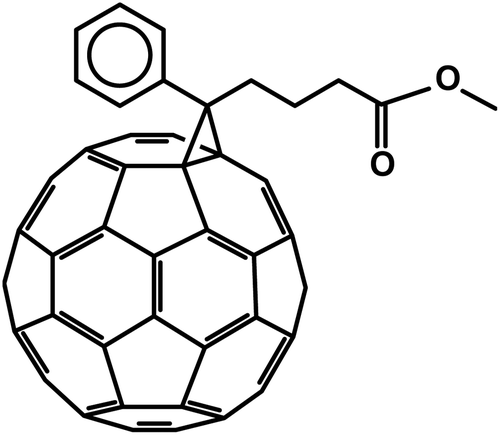 | ||
| Fig. 1 The chemical structure of phenyl-C61-butyric acid methyl ester ([60]PCBM). | ||
In such a bulk heterojunction, the aim is to achieve a length scale of the blend morphology that is similar to the exciton diffusion length; in this way exciton decay processes are dramatically reduced since in the proximity of every generated exciton there is an interface with an acceptor present, where fast dissociation takes place. Hence, charge generation takes place everywhere in the active layer. Provided that continuous pathways exist in each material from the interface to the respective electrodes, the photon-to-electron conversion efficiency can be strongly increased. In 2001, Shaheen et al.8 obtained promising results for bulk heterojunction solar cells when mixing the conjugated polymer poly(2-methoxy-5-(3′,7′-dimethyloctyloxy)-para-phenylene vinylene) (MDMO-PPV) with [60]PCBM in a 20![[thin space (1/6-em)]](https://www.rsc.org/images/entities/char_2009.gif) :80 weight percentage and optimizing the nanoscale morphology of the film, yielding a power conversion efficiency of 2.5%.
:80 weight percentage and optimizing the nanoscale morphology of the film, yielding a power conversion efficiency of 2.5%.
For an understanding of the optoelectronic properties of MDMO-PPV:[60]PCBM based solar cells, knowledge about the charge transport properties of the individual components is indispensable. For MDMO-PPV, the transport of holes has been extensively studied due to its application in polymer light-emitting diodes. From space-charge limited current (SCLC) measurements,9 transient electroluminescent measurements10 and impedance spectroscopy,11 a hole mobility μh of 5 × 10⁻¹¹ m2 V−1 s−1 has been obtained for MDMO-PPV. For the electron transport in fullerenes, a mobility was reported from field-effect measurements on thin films of evaporated C60, which typically amounts to 8 × 10⁻⁶ m2 V−1 s−1.12 For C60 single crystals grown from the vapor phase, a mobility of 5 × 10⁻⁵ m2 V−1 s−1 had been obtained from time-of-flight experiments.13 Although the first BHJ solar cell including the solution-processed [60]PCBM was published in 1995, it was not until 2003 that the electron mobility of [60]PCBM was determined. It was demonstrated by Mihailetchi et al.14 that the electron current in [60]PCBM is trap free and space-charge limited, which allows for a direct determination of the electron mobility μe from current density–voltage (J–V) measurements.
Results and discussion
Electron transport in [60]PCBM and its derivatives
The devices used by Mihailetchi et al. consisted of a single [60]PCBM layer sandwiched between a hole conducting layer of poly(3,4-ethylenedioxythiophene)/poly(styrenesulfonate) (PEDOT:PSS, Bayer AG) of typically 100 nm and an evaporated lithium fluoride (LiF) (∼1 nm)/40 nm aluminium layer (Al) top electrode. LiF forms an Ohmic contact for electron injection into [60]PCBM, whereas the work function of PEDOT:PSS (5.1 eV) does not match to the HOMO level of [60]PCBM (6.1 eV),15 such that hole injection from PEDOT:PSS into [60]PCBM can be neglected. Consequently, only electrons are expected to flow into [60]PCBM under forward bias conditions. In Fig. 2, the experimental J–V characteristics at room temperature (T = 295 K) are shown for [60]PCBM devices with layer thicknesses L of 90 nm and 170 nm.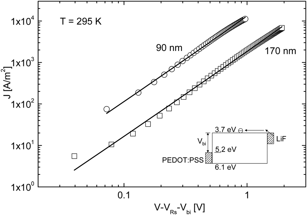 | ||
| Fig. 2 Experimental and calculated (solid lines) J–V characteristics of ITO/PEDOT:PSS/[60]PCBM/LiF/Al devices with thicknesses L = 90 nm and 170 nm (symbols), using Vbi = 1.4 eV and VRs = 30 Ω. The device band diagram is indicated in the inset. The electron transport is described by SCLC [eqn (1)] with an electron mobility μe = 2.0 × 10⁻⁷ m2 V−1 s−1 and a dielectric constant εr = 3.9 (reprinted with permission from ref. 14. Copyright 2003 Wiley-VCH Verlag GmbH & Co. KGaA, Weinheim). | ||
The voltage axis is corrected for the built-in voltage, Vbi = 1.4 eV, which arises from the different work functions of the electrodes. For applied voltages below Vbi, the electric field in the device is opposite to the current flow leading to a negative drift current, such that the current is dominated by diffusion. For voltages larger than Vbi, the electric field and current are in the same direction and now the current is drift dominated. In this region, the SCLC analysis can be applied, given by16
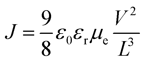 | (1) |
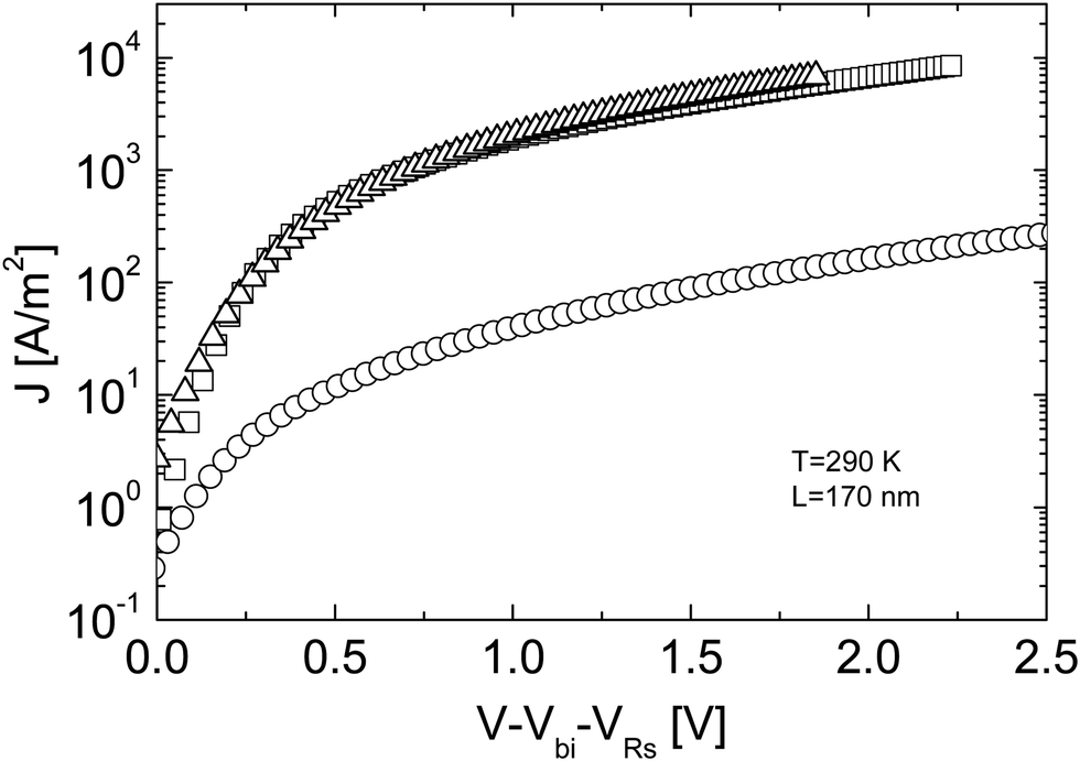 | ||
| Fig. 3 Experimental J–V characteristics of an ITO/PEDOT:PSS/MDMO-PPV:[60]PCBM (1:4)/LiF/Al solar cell device in the dark (squares), together with a [60]PCBM electron only device (triangles) and an ITO/PEDOT:PSS/MDMO-PPV:[60]PCBM/Au hole-only device (circles) with a thickness of L = 170 nm at a temperature T = 290 K. The J–V characteristics are corrected for the ITO serial resistance (VRs) and for a built-in voltage Vbi (replotted with permission from ref. 17. Copyright 2003 American Physical Society). | ||
In contrast, in order to electrostatically allow the experimentally observed photocurrents of MDMO-PPV:[60]PCBM solar cells, a hole mobility of at least 10−4 cm2 V−1 s−1 is required, which exceeds the observed hole mobility in pristine MDMO-PPV by more than two orders of magnitude.18 From space charge-limited conduction, admittance spectroscopy and transient electroluminescence measurements, a hole mobility of 2 × 10⁻⁴ cm2 V−1 s−1 was found for the MDMO-PPV phase in the blend at room temperature.18 The reason why the hole mobility in MDMO-PPV increased upon blending with an excess of [60]PCBM most likely has a morphological origin. Consequently, the charge carrier transport in a MDMO-PPV:[60]PCBM solar cell is much more balanced than previously assumed, which is a necessary requirement for the observed high fill factors of above 50%.
The presence of nearly balanced transport in the MDMO-PPV:[60]PCBM blend also opens up the possibility of realizing solution-processed ambipolar field-effect transistors. Here, the two interpenetrating networks of percolating conducting paths with both hole-transporting (MDMO-PPV) and electron-transporting capabilities ([60]PCBM) in one solution-processed blend film can be used for CMOS-like circuits.19
The typical output characteristics of a field-effect transistor based on the OC1C10-PPV:PCBM blend (see Fig. 4) demonstrate operation both in hole-enhancement and electron-enhancement modes. For high negative gate voltages, Vg, the transistor is in the hole-enhancement mode and its performance is identical to a unipolar transistor based on MDMO-PPV, with a field-effect mobility of 7 × 10⁻⁴ cm2 V−1 s−1 at Vg = −20 V. At positive Vg, the transistor operates in the electron-enhancement mode (Fig. 3b), with a field-effect mobility of 3 × 10⁻⁵ cm2 V−1 s−1 at Vg = 30 V, two orders of magnitude lower than the electron mobility in a PCBM-only transistor.
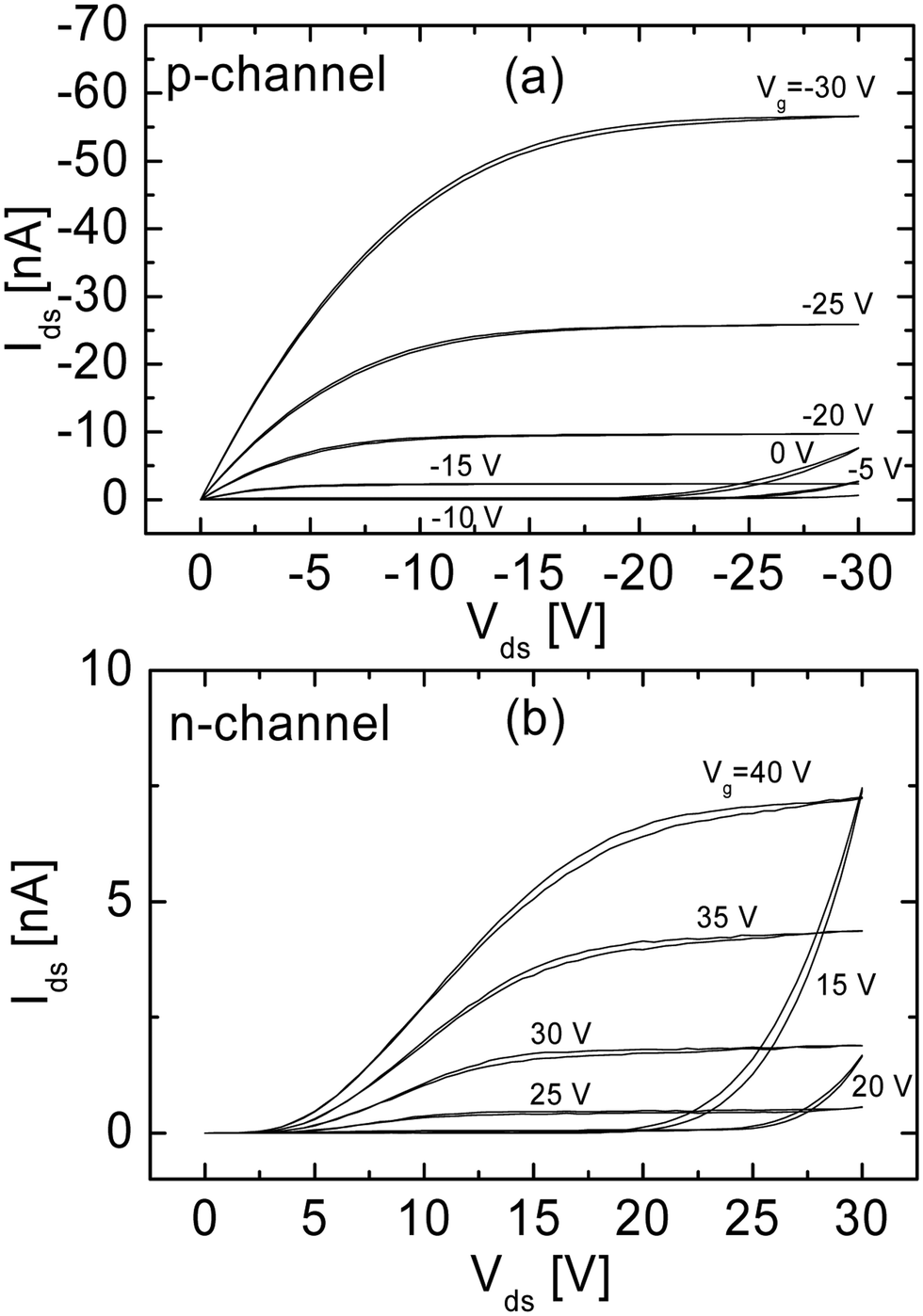 | ||
| Fig. 4 Output characteristics of the MDMO-PPV:PCBM ambipolar transistor operating in (a) the hole-enhancement and (b) electron-enhancement mode (reprinted by permission from Macmillan Publishers Ltd: Nat. Mater., ref. 19, copyright 2003). | ||
Despite being an excellent electron transporter and even improving the transport in MDMO-PPV, a disadvantage of [60]PCBM is that it is a relatively weak absorber in the visible range, thereby limiting the amount of photogenerated charges in a 20:80% MDMO-PPV:[60]PCBM blend. As a next step to further enhance the performance of these BHJ solar cells, the Hummelen group introduced another fullerene derivative, [70]PCBM.20 After successful application of the C70 derivative [70]PCBM as an alternative for [60]PCBM as the acceptor, the efficiency of solar cells with MDMO-PPV as the donor was raised to 3.0% due to the enhanced absorption of [70]PCBM as compared to that of [60]PCBM and this resulted in a higher photocurrent. From the side of the donor, regioregular poly(3-hexylthiophene) (P3HT) appeared as an attractive candidate as it combined environmental stability, reasonably high hole mobility and an improved absorption as compared with MDMO-PPV-based devices. Thermal annealing of the P3HT:[60]PCBM blend devices dramatically improves the external quantum efficiency of these cells.21–23 It is well known that an enhanced degree of crystallinity can be induced in polythiophene films by thermal annealing. This controlled crystallization and orientation of polythiophene polymer chains can significantly improve the hole mobility.24 Besides this, a red shift of the optical absorption of P3HT inside the blend is observed, providing an improved overlap with the solar emission. Furthermore, a lower amount of the weak absorbing fullerene in P3HT:[60]PCBM is required for optimized performance, typically ranging from 1:1 to 1:2 wt%, resulting in efficiencies as high as 4.0%, with external quantum efficiencies peaking at around 80% and internal quantum efficiencies surpassing 90%.25 However, when analyzing the electronic levels of the P3HT:[60]PCBM system, an important loss mechanism can be identified; the lowest unoccupied molecular orbital (LUMO) of P3HT is 1.1 eV higher than the LUMO of the acceptor. This results in a reduction of the open circuit voltage Voc, since the open-circuit voltage is ultimately limited by the difference between the HOMO of the donor and the LUMO of the acceptor.26,27 It was calculated that by raising the LUMO of the acceptor by 0.5 eV, the estimated efficiency of a single layer solar cell would be raised to 8.4%.28 To this end, a bisadduct analogue of [60]PCBM, bisPCBM, was developed by the Hummelen group. BisPCBM is normally obtained as a side product in the preparation of [60]PCBM.29 The material used for this study was obtained by standard chromatographic separation from the other reaction products and consists of a number of regioisomers, as shown in the inset of Fig. 5.
 | ||
| Fig. 5 Cyclic voltammetry measurements performed on [60]PCBM (solid line) and bisPCBM (dashed line). Experimental conditions: V vs. Fc/Fc+, Bu4NPF6 (0.1 M) as the supporting electrolyte, ODCB/acetonitrile (4/1) as the solvent and 10 mV s−1 scan rate. The inset shows the generalized chemical structure of the bisPCBM regioisomers (i.e. the bottom addend is attached in a cyclopropane manner at various [6,6] positions, relative to the top one) (reprinted with permission from ref. 30. Copyright 2008 Wiley-VCH Verlag GmbH & Co. KGaA, Weinheim). | ||
From cyclovoltametric (CV) measurements, an increase of the LUMO level of ∼100 meV of bisPCBM as compared to that of [60]PCBM was found, raising the LUMO of bisPCBM to 3.7 eV below the vacuum level.30 An important question was whether the additional functionalization of the fullerene, and the fact that the material is made up of a mixture of isomers, have any negative side effects on the charge transport properties. The electron transport through the fullerene was measured using the electron-only device ITO/PEDOT:PSS/bisPCBM/Sm/Al. Fig. 6 shows the J–V characteristics of a bisPCBM electron-only device with a thickness of 182 nm, with the applied voltage corrected for the built-in voltage and series resistance of the contact. The transport through these single carrier devices is space charge limited, resulting in a low-field electron mobility of 7 × 10⁻⁸ m2 V−1 s−1. Even though the measured electron mobility for bisPCBM is about three times lower compared to the value reported for [60]PCBM (2 × 10⁻⁷ m2 V−1 s−1), it is still expected to result in a balanced charge transport when combined with conjugated polymers such as P3HT.
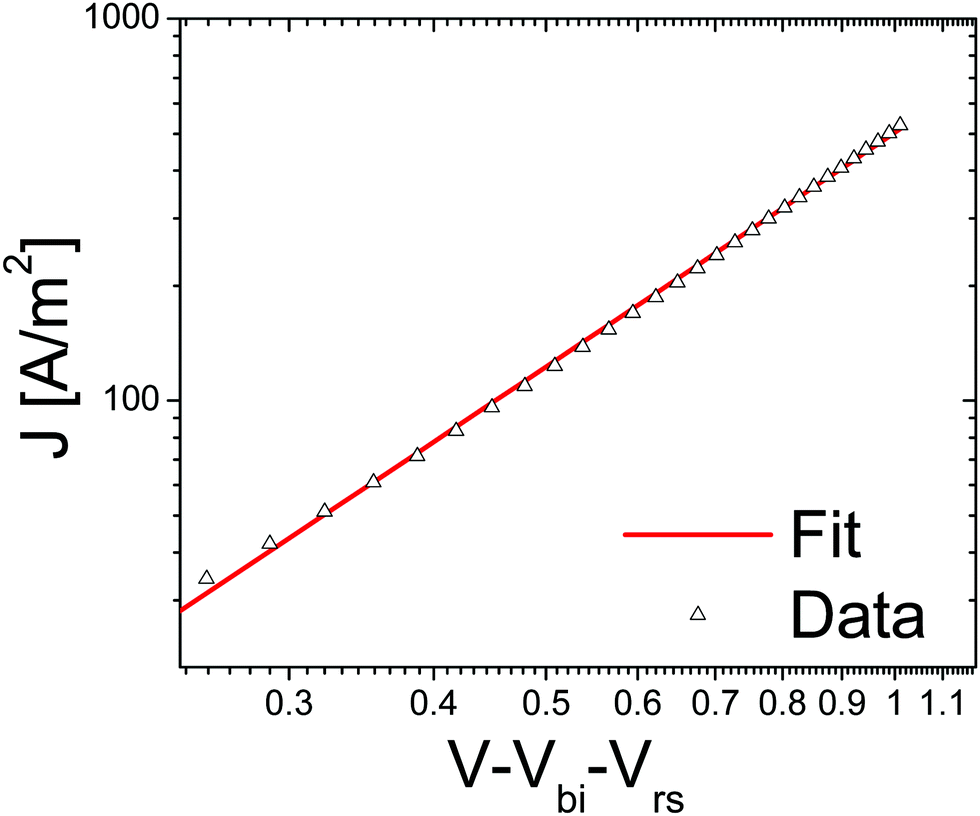 | ||
| Fig. 6 Current density vs. voltage, corrected for built in voltage and series resistance of a bisPCBM electron only device. Data (symbols) is fitted (solid line) using a space charge limited current with a mobility of 7 × 10⁻⁸ m2 V−1 s−1 (reprinted with permission from ref. 30. Copyright 2008 Wiley-VCH Verlag GmbH & Co. KGaA, Weinheim). | ||
Due to the enhanced Voc of the P3HT:bisPCBM cell of 0.73 V as a result of the reduced electron affinity, which is 0.15 V higher than that of the cell with P3HT:[60]PCBM, the resulting power conversion efficiency amounted to 4.5% for the P3HT:bisPCBM solar cell with an active area of 0.16 cm2.
As a next step, a series of higher adducts as acceptors in combination with P3HT were investigated, see Fig. 7a. In order to study the effect of this additional functionalization of the fullerene and the fact that the complete mixture of isomers – as formed in the synthetic procedure – is used, electron transport measurements have been performed on blends of P3HT and these new fullerene acceptors.31 In Fig. 7b, the J–V characteristics of electron-only devices of all the P3HT:fullerene blends at room temperature are shown. The device currents of the bisadducts are all lower compared to those of the P3HT:[60]PCBM blends, where the biggest difference occurs for the blend based on bis[70]ThCBM. For tris[60]PCBM, the electron current is even further decreased by 3 orders of magnitude, most likely due to the presence of an even higher multitude of isomers in the trisadduct. Surprisingly, in solar cells, all of the bisadducts show an almost identical device performance, such that the observed lower electron currents shown in Fig. 7b are not reflected in the solar cell performance. This can be explained by the presence of a large amount of shallow traps, originating from the various isomers. The relatively low electron-only currents for a number of bisadducts are in that case due to the fact that many electrons are immobile because they are trapped. For the solar cells, during illumination, a number of trap states will be filled, leading to an enhanced transport, and the device operation then approaches the one of the trap-free [60]PCBM device.
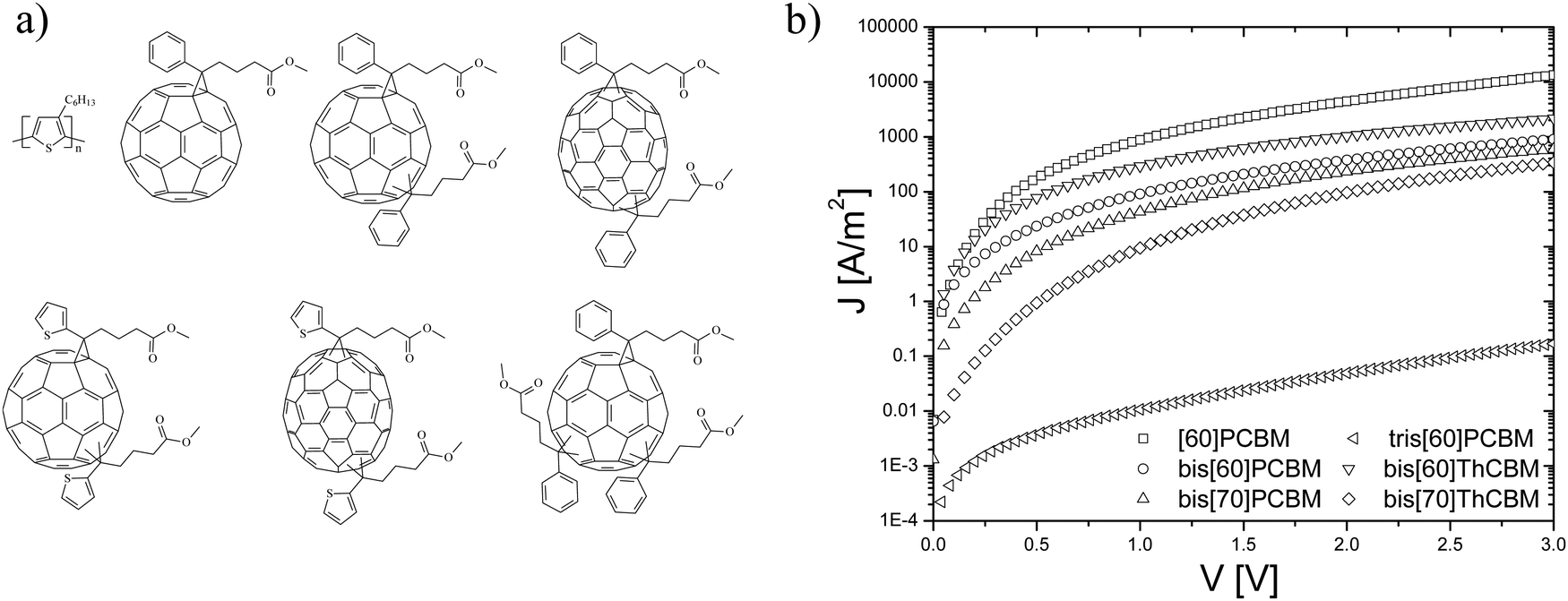 | ||
| Fig. 7 (a) Materials overview: from top left to bottom right, regioregular poly[3-hexylthiophene] (P3HT), [60]PCBM, and highly generalized structures for the isomeric mixtures of the bisadducts, bis[60]PCBM, bis[70]PCBM, bis[60]ThCBM and bis[70]ThCBM, and the trisadduct tris[60]PCBM. (b) J–V characteristics of the P3HT:fullerene blend electron single carrier devices (reprinted with permission from ref. 31. Copyright 2009 Wiley-VCH Verlag GmbH & Co. KGaA, Weinheim.). | ||
To further enhance the performance of the BHJ solar cells, an attractive option is to further increase the optical absorption of the fullerene acceptor. Replacing [60]PCBM with [70]PCBM in a fullerene:MDMO-PPV solar cell raised the efficiency from 2.5% to 3%.20 As a next step, an analogous C84 derivative has been evaluated. C84 has an even broader absorption than C70 and therefore further improvement in the current output might be expected, especially when used in combination with a relatively wide bandgap donor material like MDMO-PPV. As a first step, the electron mobility in the fullerene phase of [84]PCBM-MDMO-PPV was evaluated using the SCLC technique.32Fig. 8 shows the experimental J–V characteristics of an ITO/PEDOT:PSS/[84]PCBM:MDMO-PPV (4:1 w/w)/LiF/Al diode with thickness of 129 nm, at room temperature. From the fit of eqn (1) to the experimental data (solid line) an electron mobility for [84]PCBM of 1.0 × 10⁻³ cm2 V−1 s−1 was found, which is comparable with that of [60]PCBM. As a result, the electron transport in [84]PCBM is not expected to limit the performance of these [84]PCBM:MDMO-PPV devices. However, their efficiency only amounted to 0.25%. Most likely, in contrast to the [60]PCBM:MDMO-PPV blends, the hole mobility of MDMO-PPV is not enhanced when blended with [84]PCBM. In that case, the photocurrent will be limited by space charge, leading to a reduced fill factor and performance.
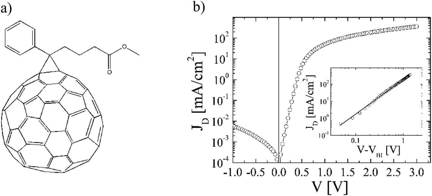 | ||
| Fig. 8 (a) Chemical structure of [84]PCBM. (b) Dark current density–voltage characteristics (JD) of an ITO/PEDOT:PSS/[84]PCBM:MDMO-PPV(4:1 w/w)/LiF/Al diode with a thickness of 129 nm at a temperature T = 295 K. The inset shows the log(JD)–log(V) characteristic corrected for the built-in voltage (Vbi = 0.31 V), together with the calculated SCLC (solid line) (replotted with permission from ref. 32. Copyright 2006 American Chemical Society). | ||
The above demonstrated versatility in tuning the electron transport, phase behavior and resulting morphology, energy levels and absorption of fullerene acceptors in BHJ solar cells is the reason why they have dominated the organic photovoltaics field for more than two decades.
Hole transport in [60]PCBM and its derivatives
As discussed in the previous section, fullerenes and their derivatives are widely used as the acceptor in BHJ organic solar cells. With regard to electron transport, fullerenes exhibit mobilities that are among the highest in organic semiconductors, which has led to their classification as “n-type” materials.33 The extent to which fullerenes are able to transport holes, on the other hand, is still a matter of debate, particularly in diode geometries. Evidence of a balanced electron and hole mobility in fullerenes has been reported for vapor-phase grown C60 single crystals, measured with the photocurrent time-of-flight technique.13 Solution-processed [60]PCBM ambipolar transistors were reported by Anthopoulos et al. with balanced electron and hole mobilities at high gate bias, even though high work function gold electrodes were employed.34 Under appropriate biasing conditions, the transistors exhibit electron and hole mobility in the order of 1 × 10⁻² cm2 V−1 s−1, and 8 × 10⁻³ cm2 V−1 s−1, respectively. Using these ambipolar transistors, a complementary-like inverter comprised of two identical ambipolar field-effect transistors based on [60]PCBM was realized.35 By contrast, in a diode configuration, measurements of the bulk mobility in [60]PCBM and [70]PCBM showed highly unipolar transport, with hole mobilities more than 6 orders of magnitude lower than the electron mobilities.36 It should be noted that, unlike transistors, for charge-transport characterization in a diode configuration, Ohmic contacts are of critical importance. In transistors, the charge injection barrier is less critical because of the image-force lowering of the injection barrier due to the gate bias at the source contact.37 To create an Ohmic contact for holes, the electrode work function should match the ionization energy (IE) of the organic semiconductor, which is in the order of ∼6 eV for most fullerenes. Typical anodes, such as indium-tin oxide and PEDOT:PSS, have work functions close to 5.0 eV,38,39 which give rise to large injection barriers with the fullerenes. Since the injected current depends exponentially on the injection barrier,40 hole-injecting electrodes with a high work function are indispensable for the creation of Ohmic contacts, enabling SCLC analysis. Recently, it was demonstrated that hole injection from high-work-function metal-oxide electrodes is improved by more than an order of magnitude using an interlayer. The requirement for this interlayer is that it has a higher IE than the organic semiconductor and that allows tunneling of charge carriers.41 Due to the presence of the interlayer, the electrode is electrostatically decoupled from the semiconductor, resulting in realignment of the Fermi level with the IE of the organic semiconductor. This method solves the problem of hole injection into organic semiconductors as fullerenes with a high IE of up to 6 eV. The fullerene derivative indene–C60 bisadduct (ICBA) was chosen (Fig. 9a) as the model material for the hole transport studies. ICBA is a bisadduct fullerene, exhibiting a HOMO and LUMO that are raised by 0.2 eV as compared to those of [60]PCBM.42 Due to this shallower HOMO (−5.9 eV), hole injection is expected to be easier compared to with [60]PCBM. To study the hole transport, hole-only devices consisting of PEDOT:PSS/ICBA/C60 (4 nm)/MoO3 (10 nm)/Al (100 nm) were constructed, with C60 (HOMO −6.4 eV) being used as the interlayer to obtain Fermi level alignment between MoO3 and ICBA.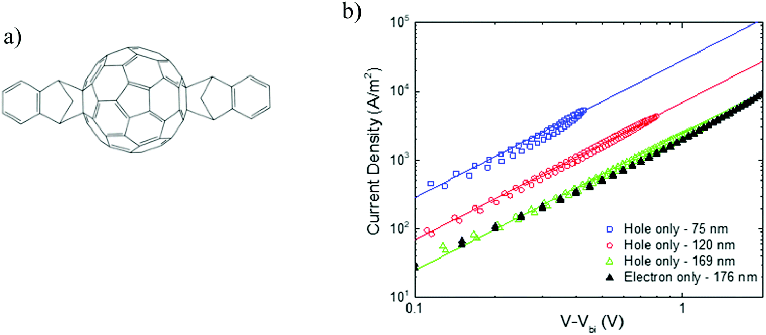 | ||
| Fig. 9 (a) Chemical structure of ICBA. (b) Current density–voltage characteristics of ICBA single-carrier devices. Hole-only devices of different layer thickness are shown (open symbols), with the voltage corrected for the built-in voltage (0.40–0.45 V) and the electrode series resistance. The solid lines are fitted with eqn (1), using a mobility of 3 × 10⁻³ cm2 V−1 s−1 for all layer thicknesses. A 176 nm thick electron-only device is plotted for comparison (closed symbols). The error (standard deviation) in the thickness was determined to be 3 to 4 nm for all films (replotted with permission from ref. 43. Copyright 2019 American Physical Society). | ||
In Fig. 9b, the measured hole current density is plotted against voltage for three different layer thicknesses. The measurements reveal that the hole current depends on the square of the voltage and scales inversely with layer thickness to the third power, as expected for SCLC. So, 16 years after the first observation of a SCLC for electrons in [60]PCBM,14 a SCL hole current has been observed in a solution-processed fullerene. This long interval mainly originates from the absence of suitable Ohmic hole contacts for fullerenes. Applying eqn (1) to the J–V characteristics results in a hole mobility of 3 × 10⁻³ cm2 V−1 s−1 for all layer thicknesses, using a dielectric constant εr = 3.9. This hole mobility is very similar to the electron mobility in the ubiquitous fullerene derivative [60]PCBM, shown in Fig. 2. To compare the hole transport in ICBA directly to the electron transport, the electron current in ICBA was measured. As shown in Fig. 9b, the electron current is nearly equal to the hole current for a device with a similar layer thickness. Using eqn (1), the electron mobility amounts to 2.7 × 10⁻³ cm2 V−1 s−1, which is nearly equal to the determined hole mobility. This demonstrates that this fullerene derivative is not an n-type transporting material but ambipolar, with equal electron and hole mobilities. This is the first observation of truly balanced and trap-free charge transport for an organic semiconductor in a diode configuration.
The ambipolarity of the charge transport in ICBA was further confirmed by the realization of a light-emitting diode (LED). A fullerene-based LED seems rather counterintuitive, since from organic photovoltaics, fullerenes are known as excellent exciton quenchers. However, as shown in Fig. 10, the ICBA LED exhibits electroluminescence, effectively operating as a light-emitting diode. The measured light output confirms the presence of both electrons and holes in the device. The external quantum efficiency for electroluminescence in the bipolar device was determined to be 1.8 × 10⁻⁵, which indicates relatively efficient electron–hole recombination due to the absence of traps when considering the low fluorescence quantum yield of fullerenes (∼7 × 10⁻⁵ for C60 films at 300 K).44
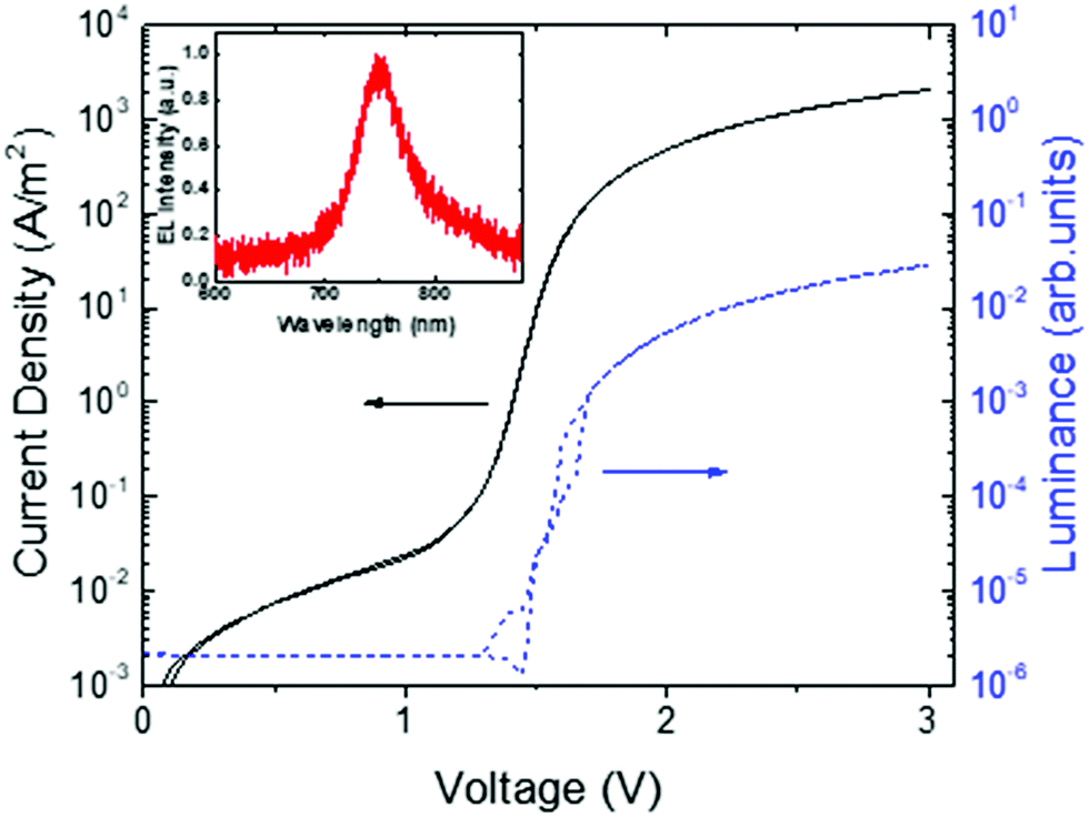 | ||
| Fig. 10 Current density and luminance vs. voltage for an ICBA light-emitting diode with an ICBA layer thickness of 118 nm. The electroluminescence (EL) spectrum is shown in the inset (replotted with permission from ref. 43. Copyright 2019 American Physical Society). | ||
An intriguing question is now whether the occurrence of ambipolar transport is valid for all fullerene derivatives. To this end, the hole transport in 3 fullerenes is compared, C60, [60]PCBM and ICBA. The functionalization of the fullerene results in a lowering of the ionization energy, ranging from 6.4 eV for pristine C60 to 6.1 eV for [60]PCBM and 5.9 eV for ICBA. As shown in Fig. 11, for C60 and [60]PCBM the current has a voltage dependence stronger than quadratic (slopes of 4.9 and 4.0, respectively), which is indicative of trap-limited hole transport and is in contrast with the trap-free transport observed in ICBA. Thus, the observed inferior hole transport in C60 and [60]PCBM is a direct result of hole trapping.
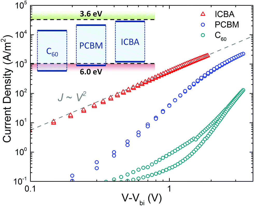 | ||
| Fig. 11 Current density vs. voltage characteristics of ICBA (213 nm), [60]PCBM (222 nm), and C60 (227 nm) hole-only devices, corrected for the built-in voltage (Vbi). The grey dashed line indicates a quadratic voltage dependence. The inset shows a schematic energy diagram, indicating the IE and EA of the fullerene derivatives with respect to the trap-free window (dashed lines) (reprinted by permission from Macmillan Publishers Ltd: Nat. Mater., ref. 45, copyright 2019). | ||
For [60]PCBM, the hole transport can also be described with a high hole mobility similar to the electron mobility, but with the addition of a relatively low concentration (1016 cm−3) of hole traps. At higher voltages (>3 V) the trap-filled limit region is reached and the quadratic slope of the J–V characteristics in this region can be described with eqn (1) using a hole mobility of approximately 10−3 cm2 V−1 s−1, again close to the earlier observed electron mobility. As a result, the intrinsic transport in [60]PCBM is also ambipolar, but the hole transport is hindered by traps. In the case of C60, even more severe hole trapping sets in, resulting in a steep J–V characteristic and the trap-filled limit is not reached in the experimental voltage range. The observation of hole trapping for fullerenes with an IE higher than 6 eV is in accordance with the observation of a trap-free energy window for charge transport.45 It was observed that when the ionization energy (IE) of a material surpasses 6 eV, hole trapping will limit the hole transport, whereas an electron affinity (EA) lower than 3.6 eV will give rise to trap-limited electron transport. When both energy levels are within this window, charge transport for both types of carriers is trap free, enabling bipolar charge transport. A possible origin for the onset of hole trapping is the presence of water clusters. The ionization energy of a water molecule is strongly reduced to ∼6 eV when the molecule is surrounded by a shell of other water molecules.
In conclusion, the charge transport properties of fullerenes have been shown to be intrinsically ambipolar, evidenced by trap-free space charge-limited electron and hole currents in the fullerene derivative ICBA. Both electron and hole mobilities are in the region of 10−3 cm2 V−1 s−1, as also observed for the electron mobility of the widely-used fullerene derivative [60]PCBM. As a result, fullerenes can also be excellent hole-transporting materials, despite being classified as ‘n-type’ materials. However, their ambipolar charge transport properties can be masked by the presence of charge trapping. With regard to electron transport, nearly all fullerene derivatives have an electron affinity above 3.5 eV, such that their electron transport is trap-free. However, electron trapping can still be observed in higher adducts due to the presence of isomers with slightly different electron affinities. The hole transport of fullerenes is limited by trapping when their ionization energy is higher than 6 eV, as is the case for [60]PCBM and C60. Fullerenes with an electron affinity and ionization energy in the trap-free window represent a unique class of organic semiconductors with trap-free and balanced high mobility electron and hole transport.
Outlook
With the rising interest in perovskite based solar cells, as well as non-fullerene acceptors in organic solar cells, one might expect that the interest in fullerenes as a charge transport material has declined. However, it has recently been realized that the hole- and electron extracting layers in perovskite solar cells play an important role in their performance, since they affect recombination losses at the interface with the perovskite. Conventional fullerenes, such as PCBM and ICBA, have been applied almost from the start as the electron transport layer (ETL) in perovskite solar cells.46 Later on, modified fullerenes using diphenylmethanofullerene moieties with oligoether chains (C70-DPM-OE) were developed in order to passivate trap states at the perovskite/fullerene interface.47 Furthermore, the preparation procedure of fullerene based ETLs was simplified by the development of a fullerene pyrrolidine derivative.48 To further enhance the conductivity and extraction properties, C60 was doped with methylammonium iodide, leading to enhanced fill factors.49 For inverted solar cells, carboxyl-functionalized C60 pyrrolidine tris-acid (CPTA) was developed, which, due to its covalent bonds to the indium-tin-oxide substrate, suppresses hysteresis in the electrical characteristics.50 By modifying the side chains of PCBM with propyl, butyl and hexyl esters, it was shown that the molecular structure of these PCBM analogs has a large impact on the ambient stability when used as the ETL in perovskite solar cells.51 By mixing PCBM with fluorocarbon chains, the moisture resistance of the ETL was also strongly improved.52 The thermal stability of the fullerene based ETL was further enhanced using a blend of PCBM and [6,6]-phenyl-C61-propylbenzene.53 Using thin layers of fullerenes with nitrogen atoms incorporated with varying basicity enhanced the electron extracting capability.54 These examples show that the field of charge transporting fullerenes is still very vivid, with many new compounds being recently developed, pushed by their application in perovskite solar cells. However, in contrast to the earlier fullerenes applied in organic solar cells as summarized in this paper, detailed charge transport studies on these novel compounds revealing charge carrier mobilities and their relation to the molecular structure are still lacking. This will be an important direction for future research.Acknowledgements
The authors acknowledge all contributions from the (former) members of the Molecular Electronics departments of the University of Groningen and the Max Planck Institute for Polymer Research over the last two decades to this work. Special thanks go out to J. C. (Kees) Hummelen for providing many of the fullerenes described in this overview and the stimulating collaboration over the years. Results of Fig. 3 were financially supported by the Dutch Ministries of EZ, O&W, and VROM through the EET Program (EETK97115). Results of Fig. 5 and 6 were part of the research program of the Dutch Polymer Institute (project no. 524).References
- S. Barth and H. Bässler, Phys. Rev. Lett., 1997, 79, 4445–4448 CrossRef CAS.
- P. G. Dacosta and E. M. Conwell, Phys. Rev. B: Condens. Matter Mater. Phys., 1993, 48, 1993–1996 CrossRef PubMed.
- R. N. Marks, J. J. M. Halls, D. D. C. Bradley, R. H. Friend and A. B. Holmes, J. Phys.: Condens. Matter, 1994, 6, 1379–1394 CrossRef CAS.
- O. V. Mikhnenko, P. W. M. Blom and T.-Q. Nguyen, Energy Environ. Sci., 2015, 8, 1867–1888 RSC.
- C. W. Tang, Appl. Phys. Lett., 1986, 48, 183–185 CrossRef CAS.
- G. Yu, J. Gao, J. C. Hummelen, F. Wudl and A. J. Heeger, Science, 1995, 270, 1789–1791 CrossRef CAS.
- N. S. Sariciftci, L. Smilowitz, A. J. Heeger and F. Wudl, Science, 1992, 258, 1474–1476 CrossRef CAS PubMed.
- S. E. Shaheen, C. J. Brabec, N. S. Sariciftci, F. Padinger, T. Fromherz and J. C. Hummelen, Appl. Phys. Lett., 2001, 78, 841–843 CrossRef CAS.
- P. W. M. Blom, M. J. M. de Jong and M. G. van Munster, Phys. Rev. B: Condens. Matter Mater. Phys., 1997, 55, R656–R659 CrossRef CAS.
- M. C. J. M. Vissenberg and P. W. M. Blom, Synth. Met., 1999, 102, 1053–1054 CrossRef CAS.
- H. C. F. Martens, H. B. Brom and P. W. M. Blom, Phys. Rev. B: Condens. Matter Mater. Phys., 1999, 60, R8489–R8492 CrossRef CAS.
- R. C. Haddon, A. S. Perel, R. C. Morris, T. T. M. Palstra, A. F. Hebard and R. M. Fleming, Appl. Phys. Lett., 1995, 67, 121–123 CrossRef CAS.
- E. Frankevich, Y. Maruyama and H. Ogata, Chem. Phys. Lett., 1993, 214, 39–44 CrossRef CAS.
- V. D. Mihailetchi, J. K. J. van Duren, P. W. M. Blom, J. C. Hummelen, R. A. J. Janssen, J. M. Kroon, M. T. Rispens, W. J. H. Verhees and M. M. Wienk, Adv. Funct. Mater., 2003, 13, 43–46 CrossRef CAS.
- C. J. Brabec, N. S. Sariciftci and J. C. Hummelen, Adv. Funct. Mater., 2001, 11, 15–26 CrossRef CAS.
- M. A. Lampert and P. Mark, Current injection in solids, Academic Press, New York, 1970 Search PubMed.
- J. K. J. van Duren, V. D. Mihailetchi, P. W. M. Blom, T. van Woudenbergh, J. C. Hummelen, M. T. Rispens, R. A. J. Janssen and M. M. J. Wienk, J. Appl. Phys., 2003, 94, 4477–4479 CrossRef CAS.
- C. Melzer, E. J. Koop, V. D. Mihailetchi and P. W. M. Blom, Adv. Funct. Mater., 2004, 14, 865–870 CrossRef CAS.
- E. J. Meijer, D. M. De Leeuw, S. Setayesh, E. Van Veenendaal, B.-H. Huisman, P. W. M. Blom, J. C. Hummelen, U. Scherf and T. M. Klapwijk, Nat. Mater., 2003, 2, 678–682 CrossRef CAS PubMed.
- M. M. Wienk, J. M. Kroon, W. J. H. Verhees, J. Knol, J. C. Hummelen, P. A. van Hal and R. A. J. Janssen, Angew. Chem., Int. Ed., 2003, 42, 3371–3375 CrossRef CAS PubMed.
- G. Li, V. Shrotriya, J. Huang, Y. Yao, T. Moriarty, K. Emery and Y. Yang, Nat. Mater., 2005, 4, 864–868 CrossRef CAS.
- F. Padinger, R. S. Rittberger and N. S. Sariciftci, Adv. Funct. Mater., 2003, 13, 85–88 CrossRef CAS.
- W. Ma, C. Yang, X. Gong, K. Lee and A. J. Heeger, Adv. Funct. Mater., 2005, 15, 1617–1622 CrossRef CAS.
- V. D. Mihailetchi, H. Xie, B. de Boer, L. J. A. Koster and P. W. M. Blom, Adv. Funct. Mater., 2006, 16, 699–708 CrossRef CAS.
- G. Dennler, K. Forberich, M. C. Scharber, C. J. Brabec, I. Tomis, K. Hingerl and T. Fromherz, J. Appl. Phys., 2007, 102, 054516 CrossRef.
- L. J. A. Koster, V. D. Mihailetchi, R. Ramaker and P. W. M. Blom, Appl. Phys. Lett., 2005, 86, 123509 CrossRef.
- C. J. Brabec, A. Cravino, D. Meissner, N. S. Sariciftci, T. Fromherz, M. T. Rispens, L. Sanchez and J. C. Hummelen, Adv. Funct. Mater., 2001, 11, 374–380 CrossRef CAS.
- L. J. A. Koster, V. D. Mihailetchi and P. W. M. Blom, Appl. Phys. Lett., 2006, 88, 093511 CrossRef.
- J. C. Hummelen, B. W. Knight, F. Lepec, F. Wudl, J. Yao and C. L. Wilkins, J. Org. Chem., 1995, 60, 532–538 CrossRef CAS.
- M. Lenes, G. A. H. Wetzelaer, F. B. Kooistra, S. C. Veenstra, J. C. Hummelen and P. W. M. Blom, Adv. Mater., 2008, 20, 2116–2119 CrossRef CAS.
- M. Lenes, S. W. Shelton, A. B. Sieval, D. F. Kronholm, J. C. Hummelen and P. W. M. Blom, Adv. Funct. Mater., 2009, 19, 3002–3007 CrossRef CAS.
- F. B. Kooistra, V. D. Mihailetchi, L. M. Popescu, D. Kronholm, P. W. M. Blom and J. C. Hummelen, Chem. Mater., 2006, 18, 3068–3073 CrossRef CAS.
- J. E. Anthony, A. Facchetti, M. Heeney, S. R. Marder and X. Zhan, Adv. Mater., 2010, 22, 3876–3892 CrossRef CAS PubMed.
- T. D. Anthopoulos, C. Tanase, S. Setayesh, E. J. Meijer, J. C. Hummelen, P. W. M. Blom and D. M. deLeeuw, Adv. Mater., 2004, 16, 2174 CrossRef CAS.
- T. D. Anthopoulos, D. M. de Leeuw, E. Cantatore, S. Setayesh, E. J. Meijer, C. Tanase, J. C. Hummelen and P. W. M. Blom, Appl. Phys. Lett., 2004, 85, 4205–4207 CrossRef CAS.
- A. Armin, S. Shoaee, Q. Lin, P. L. Burn and P. Meredith, npj Flexible Electron., 2017, 1, 13 CrossRef.
- J. J. Brondijk, F. Torricelli, E. C. P. Smits, P. W. M. Blom and D. M. de Leeuw, Org. Electron., 2012, 13, 1526–1531 CrossRef CAS.
- N. Koch and A. Vollmer, Appl. Phys. Lett., 2006, 89, 162107 CrossRef.
- M. G. Helander, Z. B. Wang, J. Qiu, M. T. Greiner, D. P. Puzzo, Z. W. Liu and Z. H. Lu, Science, 2011, 332, 944–947 CrossRef CAS PubMed.
- J. G. Simmons, Phys. Rev. Lett., 1965, 15, 967–968 CrossRef.
- N. B. Kotadiya, H. Lu, A. Mondal, Y. Ie, D. Andrienko, P. W. M. Blom and G.-J. A. H. Wetzelaer, Nat. Mater., 2018, 17, 329–334 CrossRef CAS PubMed.
- Y. He, H.-Y. Chen, J. Hou and Y. Li, J. Am. Chem. Soc., 2010, 132, 1377–1382 CrossRef CAS PubMed.
- N. B. Kotadiya, P. W. M. Blom and G.-J. A. H. Wetzelaer, Phys. Rev. Appl., 2019, 11, 024069 CrossRef CAS.
- D. R. Haynes, A. Tokmakoff and S. M. George, Chem. Phys. Lett., 1993, 214, 50–56 CrossRef CAS.
- N. B. Kotadiya, A. Mondal, P. W. M. Blom, D. Andrienko and G.-J. A. H. Wetzelaer, Nat. Mater., 2019, 18, 1182–1186 CrossRef CAS PubMed.
- J. Y. Jeng, Y. F. Chiang, M. H. Lee, S. R. Peng, T. F. Guo, P. Chen and T. C. Wen, Adv. Mater., 2013, 25, 3727–3732 CrossRef CAS PubMed.
- Y. Xing, C. Sun, H. L. Yip, G. C. Bazan, F. Huang and Y. Cao, Nano Energy, 2016, 26, 7–15 CrossRef CAS.
- R. Chen, W. Wang, T. L. Bu, Z. L. Ku, J. Zhong, Y. Peng, S. Xiao, W. You, F. Huang, Y. Cheng and Z. Fu, Acta Phys.-Chim. Sin., 2019, 35, 401–407 CAS.
- Y. Bai, Q. Dong, Y. Shao, Y. Deng, Q. Wang, L. Shen, D. Wang, W. Wei and J. Huang, Nat. Commun., 2016, 7, 12806 CrossRef CAS PubMed.
- Y.-C. Wang, X. Li, L. Zhu, X. Liu, W. Zhang and J. Fang, Adv. Energy Mater., 2017, 7, 1701144 CrossRef.
- M. Elnaggar, M. Elshobaki, A. Mumyatov, S. Y. luchkin, N. N. Dremova, K. J. Stevenson and P. A. Troshin, Sol. RRL, 2019, 3, 1900223 CrossRef.
- Z. Xing, S. H. Li, F.-F. Xie, P.-Y. Xu, L.-L. Deng, X. Zhong and S.-Y. Xie, ACS Appl. Mater. Interfaces, 2020, 12, 35081–35087 CrossRef CAS PubMed.
- S.-H. Li, Z. Xing, B.-S. Wu, Z.-C. Chen, Y.-R. Yao, H.-R. Tian, M.-F. Li, D.-Q. Yun, L.-L. Deng, S.-Y. Xie, R.-B. Huang and L.-S. Zheng, ACS Appl. Mater. Interfaces, 2020, 12, 20733–20740 CrossRef CAS PubMed.
- O. Fernandez-Delgado, P. S. Chandrasekhar, N. Cano-Sampaio, Z. C. Simon, A. R. Puente-Santiago, F. Liu, E. Castro and L. Echegoyen, J. Mater. Chem. C, 2021, 9, 10759–10767 RSC.
| This journal is © The Royal Society of Chemistry 2021 |