
 Open Access Article
 This Open Access Article is licensed under a
 Creative Commons Attribution 3.0 Unported Licence
Optical properties of orthorhombic germanium selenide: an anisotropic layered semiconductor promising for optoelectronic applications†
Agata
Tołłoczko
 *a,
Szymon J.
Zelewski
a,
Michał
Błaszczak
a,
Tomasz
Woźniak
a,
Anna
Siudzińska
b,
Alicja
Bachmatiuk
b,
Paweł
Scharoch
a and
Robert
Kudrawiec
ab
*a,
Szymon J.
Zelewski
a,
Michał
Błaszczak
a,
Tomasz
Woźniak
a,
Anna
Siudzińska
b,
Alicja
Bachmatiuk
b,
Paweł
Scharoch
a and
Robert
Kudrawiec
ab
aDepartment of Semiconductor Materials Engineering, Wrocław University of Science and Technology, Wybrzeże Wyspiańskiego 27, 50-370 Wrocław, Poland. E-mail: agata.tolloczko@pwr.edu.pl
bŁukasiewicz Research Network – PORT Polish Center for Technology Development, Stabłowicka 147, Wrocław, Poland
First published on 28th September 2021
Abstract
Group-IV monochalcogenides, such as germanium selenide (GeSe), are strongly anisotropic semiconducting van der Waals crystals isoelectronic to black phosphorus, with superior stability in air conditions. High optical absorption, good conductivity, and band gap ranging from 1 to 2 eV make these materials suitable for various optoelectronic applications; however more in-depth investigation of their fundamental properties is required. We present a comprehensive study of bulk GeSe by means of optical absorption and modulation spectroscopy, supported by theoretical density functional theory (DFT) calculations of the electronic band structure. Our experimental results reveal that the optical properties of GeSe are dominated by direct transitions; however the fundamental band gap might in fact be indirect and could not be observed in the experiment due to low oscillator strength. Such interpretation is in agreement with our calculations, providing the picture of the first Brillouin zone with multiple band extrema in close energy proximity. In order to investigate the anisotropy of the material, polarization-resolved measurements have been performed, revealing a strong dependence of the observed optical transitions on light polarization. Photogenerated current measurements resulted in reasonably high photoconversion efficiency and fast response time, implying that GeSe is a promising material for photoconversion applications.
Introduction
Since the interest in two-dimensional (2D) materials and heterostructures has been boosted by the first successful exfoliation of atomically thin graphite flake, graphene,1,2 a variety of other layered van der Waals crystals have been rediscovered as potentially more suitable for certain applications than semimetallic graphene. One of them is black phosphorus (BP), a promising direct band gap semiconducting material, which in analogy to graphene is called phosphorene in its monolayer form. BP is known to fill the gap between graphene and transition metal dichalcogenides (TMDs) – it combines open energy gap, characteristic for TMDs, with excellent conductivity, nearly comparable to graphene.3–5 Unfortunately, despite being the most stable phosphorus allotrope, BP is prone to oxidation in air conditions, which severely limits its applications.6,7Group IV monochalcogenides (MX, where M is a group IV element, such as Ge, Sn or Pb, and X is a chalcogen atom, such as S, Se, or Te) are a family of van der Waals crystals isoelectronic to black phosphorus, which are also known as phosphorene analogues,2,8 as they share the most important features, but exhibit superior stability. MXs are semiconductors with an orthorhombic crystal structure (space group Pcmn). Atomic arrangement along main in-plane crystallographic directions is strongly anisotropic, which affects the material's fundamental properties.9–14 An open band gap tunable from the near infrared to visible spectral range, high carrier mobility, and strong optical absorption make MXs perfect candidates for application in two-dimensional optoelectronics (photovoltaics, light detectors and emitters).15–19 They do, however, exhibit other properties that can be exploited in different areas of technology, such as nonlinear optics,20–23 transistors,24,25 piezotronics,26–28 multiferroics-based devices,29–32 or photocatalytic water splitting.33–36
Germanium selenide (GeSe) has attracted the particular interest of researchers focused on photovoltaics.15,16,37–40 The material exhibits low toxicity and is composed of earth-abundant elements. In its bulk form, the band gap of GeSe is most often reported between 1.1 and 1.3 eV (dependent on the experimental or theoretical method), which is close to the optimal value for maximum photoelectric conversion, according to the Shockley–Queisser detailed balance limit.41 Moreover, it is possible to combine GeSe with other van der Waals crystals, especially group IV mono- and dichalcogenides, to form heterostructures,42–45 which can be exploited as p–n-like junctions, due to relative band offsets,46 or in the construction of tandem solar cells. With the selenium-rich analogue of GeSe, GeSe2,47,48 such heterostructure can be grown in one reaction chamber using the same precursors but by adjusting only the stoichiometric ratio, which allows the avoidance of impurities and unintentional doping, as reported for the SnSe/SnSe2 heterostructure.49 The CVD technique can also be exploited, which is important for large-scale device integration.
To date, there are a lot of discrepancies in the literature concerning the optical and electronic properties of GeSe, particularly the character and exact width of the fundamental band gap, crucial for the design of any semiconducting device. Based on the experimental investigation of the optical activity in GeSe, the majority of authors report an indirect fundamental band gap of ∼1.2 eV at room temperature.50–53 However, there are also reports of a direct band gap at slightly higher energies.37 The reason for numerous various interpretations can be found in the electronic band structure, featuring flat bands and multiple band extrema within close energy proximity, characteristic of the whole MX family.8,15,46 Unfortunately, density functional theory (DFT) calculations do not provide the unambiguous answer as well, as the width of the fundamental band gap of GeSe and its position in the Brillouin zone (BZ) are sensitive to lattice parameters and the computation method in general.8,37,50,54,55
In this work we present a comprehensive study of GeSe focused on its optical properties, anisotropy, and photoelectric conversion efficiency. The samples were characterized by high resolution transmission electron microscopy (HRTEM), selected area electron diffraction (SAED), electron energy loss spectroscopy (EELS), and Raman spectroscopy. The optical properties of GeSe were investigated using polarization- and temperature-resolved optical absorption and photoreflectance (PR), one of the methods of modulation spectroscopy. Optical absorption reveals the fundamental band gap of the material (either direct or indirect), while PR allows observation of energetically higher features, but it is only sensitive to direct optical transitions. Therefore, the two methods are considered complementary. Ab initio calculations of the electronic band structure have been performed to support experimental results and enable assignation of the measured optical transitions to certain BZ points. Eventually, the photoelectric conversion efficiency of a simple GeSe zero-bias photodetector has been studied, by means of photogenerated current measurements.
Results and discussion
Germanium selenide crystallizes in the orthorhombic phase (Pcmn), schematically presented in Fig. 1a. The lattice constants are a = 0.444 nm, b = 0.386 nm, and c = 1.081 nm,56 where a and b are in-plane unit cell dimensions, and c is the lattice parameter perpendicular to the layer plane. DFT calculations yield a = 0.442 nm, b = 0.389 nm, and c = 1.092 nm, in excellent agreement with measured values. The atomic structure within a single layer is anisotropic. In the x (100) direction, called armchair, the layer is puckered, while in the orthogonal y (010) direction, called zigzag, the atoms are arranged in a ladder-like pattern. As can be seen in the HRTEM image and the SAED pattern presented in Fig. 1b and c, respectively, the investigated sample exhibits high crystallinity. In the HRTEM image the atomic sites are clearly visible, and an arrangement characteristic of the orthorhombic phase can be observed. The spacings between crystal planes in (100), (010), and (110) directions are 0.44, 0.36, and 0.29 nm, respectively. The atomic composition of the sample was determined by EELS measurements (Fig. 1c). In the obtained spectrum edges related to Ge and Se can be distinguished. The positions of the observed L–Ge edges, along with L–Se edges, are in perfect agreement with reference values.57 The exact energies are listed in Table S1 of the ESI.† No other significant EELS features have been observed, indicating a low level of impurities in the crystal structure. In the Raman scattering spectrum (Fig. 1f) two peaks at frequencies of 152 cm−1 (19 meV) and 189 cm−1 (23 meV) are clearly visible. These modes can be assigned to B3g and Ag symmetries, corresponding to in-plane shear vibrations of adjacent layers in the y and x directions, respectively.58 Two other Raman peaks at frequencies of 81 and 176 cm−1 are often reported,59,60 but have not been observed in our measurements. | ||
| Fig. 1 (a) Schematic illustration of the GeSe orthorhombic crystal structure and atomic arrangement along main in-plane directions (armchair and zigzag), (b) HRTEM image of the GeSe flake with crystallographic directions and spacings between crystal planes marked, (c) SAED pattern with labeled reflexes corresponding to certain crystal planes, (d) EELS spectrum with labeled edges related to Ge and Se atoms, and (e) Raman scattering spectrum, acquired for a bulk GeSe sample with the excitation of a 532 nm laser beam, at room temperature. | ||
Experimental investigations of the optical properties of GeSe reported in the literature exploit mostly optical absorption measurements, and the results are commonly perceived as the evidence of the indirect fundamental band gap between 1.10 and 1.25 eV (at room temperature).50–53 Such interpretation is supported by the lack of photoluminescence emission from bulk GeSe, although other mechanisms may be responsible for photoluminescence quenching, such as intrinsic defects, creating paths of nonradiative recombination. However, Murgatroyd et al.37 claim that the low-energy region of the absorption coefficient spectrum, previously attributed to the fundamental band-gap, in fact originates from defect-related absorption. The actual absorption edge occurs at ∼1.3 eV, and above this energy the absorption coefficient spectrum is dominated by direct optical transitions due to higher oscillator strength. Nevertheless, the authors do not negate the presence of energetically close indirect transitions or state the character of the fundamental band-gap.
In our research, in order to experimentally verify the band gap nature of GeSe, along with optical absorption a complementary spectroscopic method, photoreflectance, was exploited. In Fig. 2, photoreflectance and optical absorption spectra collected at 20 K (panel a) and 300 K (panel b) are presented. The shaded areas correspond to moduli of observed PR resonances. Low-temperature PR spectra exhibit three strong optical transitions, namely E1, E2, and E3. At room temperature only two closely lying transitions can be distinguished. The step-like shape of the absorption curve also indicates the contribution of multiple optical transitions. The sharp rise of the absorption coefficient at an energy of ∼1.3 eV at 20 K and ∼1.2 eV at 300 K coincides with the energetically lowest PR resonance. Since photoreflectance is a method sensitive only to direct transitions, such agreement suggests the direct character of the band-gap of GeSe, or that a weak absorption edge from the fundamental indirect band-gap is predominated by a stronger signal from closely lying direct optical transition.
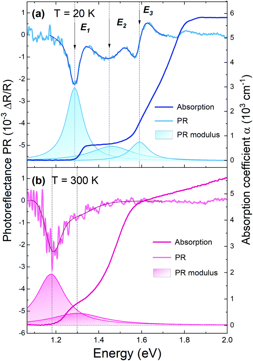 | ||
| Fig. 2 Photoreflectance and optical absorption spectra of GeSe obtained at a temperature of 20 K (a) and 300 K (b), with assigned optical transitions. The darker solid lines over the PR plots are the curves fitted with the Aspnes formula (eqn (1)), and the colored areas beneath are the PR resonance moduli, calculated using eqn (2). | ||
The exact energies of the observed PR resonances were determined by fitting the Aspnes formula61 to experimental data,
 | (1) |
 | (2) |
The area under the modulus curve, given by Ai = π|Ci|/Γi, is proportional to the transition oscillator strength.
In order to further investigate the influence of temperature on optical properties of GeSe, both PR and optical absorption were measured at different temperatures, covering the range from 20 up to 300 K. The results are presented in Fig. 3 (in panels a and b every second measured spectrum is plotted for clarity). The temperature dependence of PR (Fig. 3a) reveals that the energetically highest transition E3, narrow and well defined at 20 K, diminishes rapidly with increasing temperature, to vanish completely at 100–120 K. Such a shape and behaviour suggest excitonic transition and allows one to estimate an exciton binding energy of 10 meV; however other factors can affect the transition strength (such as slightly band-nesting character of the transition, which will be discussed later) and the exciton binding energy may actually be higher. Above 120 K E3 could still be optically active as a weaker band-to-band transition, with intensity below the detection threshold. Transitions E1 and E2 are still visible at room temperature, although due to increased broadening and a significantly larger E2 temperature coefficient (see Fig. 3c), they blend together and become hard to distinguish.
 | ||
| Fig. 3 Photoreflectance (a) and optical absorption (b) spectra measured at different temperatures from 20 to 300 K, and the temperature dependence of the optical transition energies observed in PR (diamond symbols) and absorption (circles), fitted with the Bose–Einstein formula given by eqn (3) (solid lines) (c). | ||
In the absorption spectra (Fig. 3b) two sharp edges are visible. The energies of the edges were determined from extrapolation of linear approximation of a Tauc plot for direct allowed optical transitions ((αhν)2vs. hν)62 (see Fig. S1 in ESI†). Both values and temperature dependence of lower and higher absorption edge energies are in good agreement with transitions E1 and E3 observed in photoreflectance, as can be seen in Fig. 3c. The reason why E3 is visible in absorption spectra throughout the whole temperature range may be due to the fact that only the signal from the band-to-band component was detected (no characteristic excitonic features are present in the absorption spectra). The same phenomenon could be responsible for the shift between E1 energies determined from PR and absorption (however only at low temperatures; above 180 K the uncertainty of the PR resonance energy increases rapidly due to noise and proximity of E2).
The temperature dependencies of each transition energy were approximated by Bose–Einstein63 (solid lines in Fig. 3c) and Varshni64 (not shown in the figure) formulas. The B–E approximation is derived from the Bose–Einstein distribution and is defined as
 | (3) |
 | (4) |
The Varshni equation is commonly used for temperature dependence approximation; however the parameters in the formula have no direct physical interpretation and can only be used for empirical comparison. On the other hand, the B–E formula includes parameters that are dependent on material properties and follow the low-temperature experimental data with better accuracy. The fitting parameters from both methods are listed in Table 1. It is worth noting that the average phonon temperature between 202 and 205 K, corresponding to a thermal energy of 18 meV, coincides perfectly with the first Raman peak in the measured spectrum (Fig. 1e) and is close to average phonon energy determined using other methods (phonon dispersion calculations, Raman scattering).60,65–67
| Transition | Varshni | Bose–Einstein | ||||
|---|---|---|---|---|---|---|
| E(0) (eV) | α (10−4 eV K−1) | β (K) | E(0) (eV) | a B (meV) | θ B (K) | |
| E 1 | 1.451 ± 0.039 | 9.91 ± 0.45 | 245 ± 51 | 1.448 ± 0.036 | 76.4 ± 7.7 | 206 ± 32 |
| E 2 | 1.583 ± 0.013 | 9.20 ± 0.69 | 229 ± 39 | 1.580 ± 0.010 | 71.5 ± 7.2 | 202 ± 10 |
| E 3 | 1.292 ± 0.012 | 5.01 ± 0.14 | 225 ± 45 | 1.290 ± 0.013 | 40.0 ± 4.1 | 205 ± 16 |
To explore the anisotropy of the optical activity of GeSe, a series of polarization-dependent measurements were performed. Photoreflectance and optical absorption were measured as a function of the linear polarization angle of the incident light parallel to the sample surface. In the orthorhombic crystal structure of GeSe two main in-plane orthogonal directions can be discerned – armchair and zigzag. As can be seen in Fig. 4a, in the PR spectrum acquired for armchair polarization only two out of three optical transitions are visible – E1 and E3. While rotating the polarization towards zigzag, E1 and E3 weaken to disappear entirely, and E2 emerges. The polarization dependence is best visible in Fig. 4c, where the polar plot of the area under PR modulus curve (calculated using eqn (2)) is presented for transitions E1, E2 and E3. The dependence was fitted with a formula derived from Malus’ law,
| f(φ) = f‖cos2(φ − φ0) + f⊥sin2(φ − φ0), | (5) |
 | (6) |
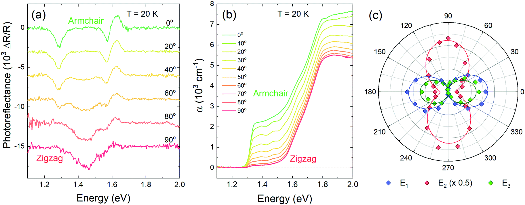 | ||
| Fig. 4 Photoreflectance (a) and optical absorption (b) spectra acquired for light polarized linearly from 0° (along the armchair crystallographic direction) to 90° (along the zigzag direction). Polarization dependence of transition oscillator strength, calculated as the integrated area under the PR resonance modulus curve (c). | ||
Absorption spectra are sensitive to polarization as well, as shown in Fig. 4b. The energetically lower absorption edge, corresponding to transition E1, is best visible for the armchair polarization. The second component, attributed to transition E3 based on temperature-dependent measurements, does not change significantly with the polarization, which is inconsistent with the PR results. Assuming the interpretation that in absorption spectra the band-to-band transition is visible, while the PR resonance is of excitonic nature, such discrepancy can be explained if the polarization selection rules do not apply to inter-band transition as strictly.
The experimental results can be further analysed and interpreted in terms of the electronic band structure of GeSe, in order to assign the observed optical transitions to certain Brillouin zone points and determine the position of the fundamental band gap. The DFT study revealed two competing valence band maxima (at the Γ point and on the Γ–X path) and three conduction band minima (at the Γ point, on the Γ–X and Γ–Y path), with relative energy dependent on the choice of the computation method and parameters.8,37,50,54,55 In this work, theoretical calculations of the GeSe band structure were performed with the use of the mBJ-TB09 potential, which is proven to give satisfactory results for similar materials.68 In Fig. 5a the Brillouin zone of GeSe is presented, with high symmetry points and directions marked. Fig. 5b shows the electronic band dispersion on high symmetry paths in the Brillouin zone. The valence band maximum (VBM) occurs on the Γ–X path, while the conduction band minimum (CBM) is at the Γ point. As a consequence, the fundamental band gap of GeSe (yellow arrow labelled E0 in the figure) is indirect, with an energy of 0.99 eV. No absorption close to this energy was observed in the experiment, indicating that either the energy is underestimated, or the transition is not optically active. Optical transitions measured experimentally and discussed in this work were assigned to certain BZ points, based on their energy and polarization. To determine the theoretical polarization of each transition, the square of the transition matrix element (Pcv2) between the topmost valence and lowermost conduction bands was calculated on a path in the BZ. Its components in armchair and zigzag directions are presented in Fig. 5c as green and orange areas, respectively. The theoretical DOP can be calculated using eqn (6), treating f‖ and f⊥ as matrix element components parallel and perpendicular to the transition polarization direction. In Fig. 5c additionally the distance between the valence and conduction band (direct band gap) is plotted (solid dark blue line, right axis), to better illustrate the critical points of the electronic band structure.
 | ||
| Fig. 5 (a) Schematic illustration of the BZ, with high symmetry points marked, (b) electronic band dispersion simulated with the mBJ-TB09 potential, along the high-symmetry path in the BZ, with optical transitions marked by arrows, (c) squared transition matrix element components in armchair (green areas) and zigzag (orange areas) directions, and the calculated distance between the valence and conduction band (solid dark blue line). | ||
The lowest direct transition E1 (blue arrow in the figure) was assigned to the point close to the VBM, on the Γ–X path, where the armchair component of the matrix element is high. The theoretical energy of this transition is 1.26 eV, which is very close to the experimental value of 1.29 eV (at 0 K, extrapolated from the temperature dependence). Although a similar energy is observed at Γ, the matrix element around this point is nearly zero. The second direct transition E2 (red arrow) was assigned to a point on the Γ–Y path, due to the high zigzag matrix element component. The distance between bands at this point is 1.78 eV. In this case, the experimentally determined energy of 1.52 eV is significantly smaller; however it is the lowest allowed transition with confirmed zigzag polarization in the BZ. The discrepancy is most likely due to underestimation of the valence band energy by the calculations or high exciton binding energy. A similar observation has been reported and discussed for GeS.68 Transition E3 (green arrow), based on its armchair polarization, can be assigned to both Y–S and Z–U paths, although the energy matches the latter better. In the Z–U direction the distance between bands is 1.68 eV, slightly higher than the experimental energy of 1.58 eV. Experimental and theoretical energies and polarizations of each transition are presented in Table 2. Worth noting is also the band-nesting (van Hove singularity of the second type) character of each direct transition – valence band maxima and the corresponding conduction band minima do not occur at exactly the same energy, as can be seen in Fig. 5b. The difference is not significant at 0 K (as provided by DFT calculations); however it may extend and have serious consequences when the influence of the temperature is considered. One of them can be the aforementioned vanishing of the PR resonance corresponding to transition E3 at ∼120 K.
| Transition | Assignation | Energy (eV) | Polarization, DOP | ||
|---|---|---|---|---|---|
| Experiment | Calculation | Experiment | Calculation | ||
| E 0 | Γ–Y→ Γ | 0.99 | — | — | |
| E 1 | Γ–Y | 1.29 | 1.29 | Armchair, 80% | Armchair, 90% |
| E 2 | Γ–X | 1.52 | 1.78 | Zigzag, 73% | Zigzag, 83% |
| E 3 | Z–T | 1.58 | 1.68 | Armchair, 76% | Armchair, 93% |
Additional DFT calculations of transition energies were performed with the HSE06 hybrid functional. Table S2 (see ESI†) presents comparison of experimental and calculated transition energies. It is clear that HSE06 significantly overestimates all the energies, while mBJ-TB09 yields much better agreement with measured values. This is in line with previous observations for another orthorhombic monochalcogenide, GeS.68
In order to investigate the functionality of GeSe in photoconversion applications, photocurrent (PC) measurements have been performed. In Fig. 6a the spectral dependence of generated photocurrent is presented (solid line), along with optical absorption (dashed line), measured at 20 K. The incident light power density used for the measurement was ∼600 mW cm−2, resulting in a photocurrent of an order of magnitude of pA. As can be seen in the figure, the absorption edge and step-like profile are in excellent agreement for both spectra. In PC a wide extremum occurs below the absorption edge, which can be attributed to ionized defects. Such conclusion has been made based on polarization dependent measurements (Fig. S2a in ESI†), revealing that above the absorption edge PC follows the optical absorption dependence on polarization, while in the energetically lower region the signal remains unchanged. It is best visible in panel b of Fig. S2 (ESI†), where the degree of polarization of the photocurrent is plotted. Below 1.3 eV the DOP is close to zero (the negative values originate from measurement artefacts and are not physical), indicating that there are no polarized features in this spectral region. As the optical properties of GeSe are strongly anisotropic (which is confirmed by theoretical calculations of the matrix element components across the Brillouin zone, presented in Fig. 5b), only defect states, insensitive to polarization, can contribute to light absorption and photocurrent generation. For energies above the absorption edge the polarization degree increases rapidly up to ∼80%, which coincides with the value of DOP extracted from the photoreflectance spectra analysis. In Fig. 6b time-resolved photocurrent response obtained for three illumination powers (10 mW, 5 mW, and 1 mW) is plotted. The 532 nm laser beam was modulated at a frequency of 80 Hz. In the bottom panel of Fig. 6b a close-up of the photocurrent decay is presented. As can be seen from the figure, after the illumination is turned off, the photocurrent drops down to 10% of its maximal value in less than 80 μs. Such rapid decay is evidence of the fast response of the device (compared to other reports for this material system18,24,65). Fig. 6c and d show the photocurrent dependence on the illumination power density and modulation frequency, respectively, measured for two laser wavelengths: 405 nm and 532 nm. The power density dependence (panel c) follows the power law in nearly the whole investigated range. Above ∼1 W cm−2 the experimental data drift from the trend, as the photocurrent saturates at the value exceeding 100 nA (for an excitation wavelength of 532 nm), which is an excellent result for a measurement in zero-bias conditions. The photocurrent generated under 405 nm laser illumination is generally lower, due to the descent of the spectral characteristics. In the PC vs. frequency plot (panel d) the current is reduced by half at a frequency of ∼50 kHz. This value is in good agreement with the estimated decay time (within the order of magnitude).
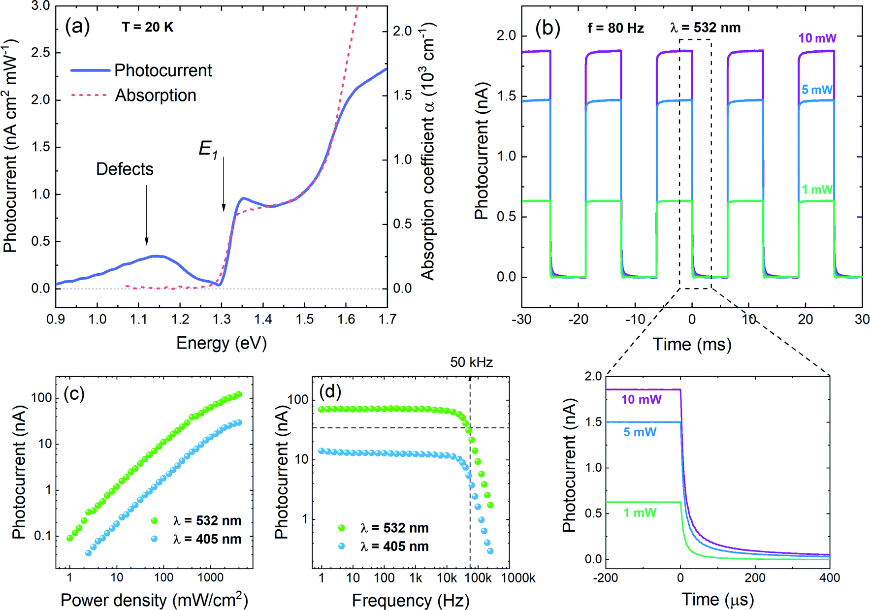 | ||
| Fig. 6 (a) The comparison of the spectral characteristics of the photocurrent (solid line) and optical absorption (dashed line) of the GeSe sample under illumination with a monochromatic light of power density ∼600 mW cm−2, (b) the photocurrent time response measured under illumination with a 532 nm laser beam modulated at a frequency of 80 Hz, at an excitation power of 1, 5, and 10 mW. In the bottom panel the decay of the photocurrent can be seen more closely, allowing the estimation of the decay time. The dependence of photocurrent on (c) light power density and (d) frequency, measured for excitation wavelengths of 532 and 405 nm. | ||
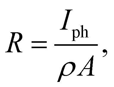
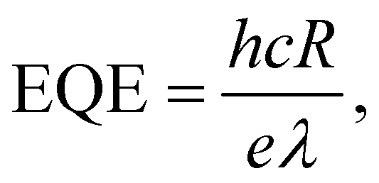
From the photocurrent measurement results, parameters commonly used to describe the efficiency of photoelectric conversion can be derived: photoresponsivity (R) and external quantum efficiency (EQE). Photosensitivity is defined as the photocurrent generated per unit illumination power and is given by
 | (7) |
 | (8) |
Conclusions
In conclusion, the optical activity and anisotropy of a group-IV monochalcogenide, GeSe, have been investigated experimentally, exploiting two complementary methods of optical spectroscopy – optical absorption and photoreflectance. The measurements have been supported by density functional theory (DFT) calculations of the electronic band structure. The experimental study exposed that the absorption properties of GeSe are dominated by direct optical transitions, suggesting the direct character of the fundamental band gap, at an energy of (1.21 ± 0.05) eV at room temperature. Additionally, two energetically higher optical transitions have been observed. Polarization-resolved measurements revealed strong anisotropy of the acquired spectra, with the polarization degree of each observed transition exceeding 70% in one of the main in-plain crystallographic directions. The experimental results are in agreement with the theoretical study, although according to DFT calculations the fundamental band gap of GeSe is indirect, at slightly lower energy than that of the lowest direct transition. Such inconsistency can be explained by the fact that the indirect transition is significantly weaker and in the experiment may not be possible to discern from the closely lying direct transition, characterized by higher oscillator strength. Therefore, the fundamental band gap of GeSe may in fact be indirect, but with the lowest direct transition within close energy proximity.Finally, we performed an investigation of the photoelectric properties of GeSe, by means of photocurrent measurements. The obtained photoresponsivity of 0.63 mA W−1 and external quantum efficiency of 0.15% are satisfactory, considering the experimental conditions (zero-bias) and the simplicity of the exploited setup. The fast response of the device (both rise and decay time of the photocurrent) is an excellent result, promising for application in photodetection technology.
We believe that our research will contribute to the general knowledge of the fundamental properties of van der Waals crystals and provide the background essential for future development of two-dimensional optoelectronics.
Methods
Experimental details
The investigated samples were bulk GeSe crystals, grown by the flux method, and were purchased from the 2D Semiconductors company (USA).56 Crystals’ purity was over 99.995%, as confirmed by XRD and EDX data provided by the manufacturer. For optical measurements flakes of thickness between 10 and 100 μm and lateral dimensions of ∼2 mm were selected. The top layer of each sample was exfoliated with Kapton tape in order to obtain a clear surface. For photocurrent measurements a larger (5 mm) and thicker (500 μm) sample was used.Structural characterization of GeSe samples was performed using high resolution transmission electron microscopy, selected area electron diffraction, and electron energy loss spectroscopy. HRTEM images and SAED patterns were acquired using a double-aberration corrected FEI Titan3 60-300 (S)TEM microscope. GeSe crystals were mechanically exfoliated onto a carbon lacey grid and subsequently imagined at an accelerating voltage of 300 kV, with spherical aberration correction. EELS analysis was performed in the STEM mode, using a Gatan Continuum (model 1077) EELS spectrometer, under the following experimental parameters: operating voltage 300 kV, beam current 120 pA, 5 mm of EELS aperture size, and dispersion of 0.3 eV ch−1.
Raman scattering measurements were performed on the micro-PL setup, consisting of a 550 mm focal length grating monochromator coupled with a liquid nitrogen cooled CCD array detector camera and a 532 nm laser line (output power 50 μW). A 50×, NA = 0.55 magnifying objective lens was used to focus the laser beam and collect the light scattered at the sample surface. Raman characterization was conducted in the backscattering mode at room temperature and under ambient conditions.
Photoreflectance (PR) and optical absorption measurements were performed using dedicated optical setups. The sample was mounted inside a cryostat connected to a closed-cycle helium cryocooler, to allow measurements from room temperature down to 20 K. For both measurements a quartz tungsten halogen (QTH) lamp was used as the white probing light source. The signal was detected with a Si photodiode and a lock-in amplifier (Stanford Research Systems SR830). For PR measurements, a 405 nm laser modulated by a mechanical chopper at a frequency of ∼300 Hz was employed. For polarization-resolved measurements a Glan–Taylor calcite linear polarizer and an achromatic half-wave plate were placed in the optical axis.
In order to investigate the photoelectric response of GeSe, photocurrent measurements were performed. The sample was mounted on a sapphire substrate (1 mm thick) to provide good thermal conduction (allowing low-temperature measurements) and electric insulation from the cold head. Four silver electric contacts were deposited on each corner of the sample. The measurements were performed under zero-bias conditions, with a Stanford Research Systems SR570 transconductance preamplifier to convert the generated photocurrent to a corresponding voltage signal, further demodulated with a lock-in amplifier. For spectral dependence measurements a mechanical chopper was used to modulate the incident light. For power, frequency, and time dependence, laser beams (405 and 532 nm) were modulated with acoustooptic modulators (AA Optoelectronics). The photocurrent time response was acquired using a high-resolution (10 bit) digital signal oscilloscope (Rohde & Schwarz RTB2000 series).
Computation details
Calculations employing DFT were performed with the use of the Vienna Ab Initio Simulation Package (VASP).70 Atomic cores were represented by relativistic projector-augmented wave (PAW) datasets71 within the Perdew–Burke–Ernzerhof (PBE) parametrization of the generalized gradient approximation (GGA) to the exchange–correlation functional.72 The geometric structure was optimized until interatomic forces were lower than 0.01 eV A−1 which resulted in stress tensor components lower than 0.5 kbar. A semi-empirical vdW correction of Tkatchenko and Scheffler was used.73 Convergence tests revealed that a plane wave basis cutoff of 650 eV combined with a 10 × 8 × 4 Monkhorst Pack k-point grid is sufficient for convergence of lattice constants up to 0.01 A. The PBE functional is commonly known to underestimate the electronic band gap; therefore the modified Becke–Johnson (mBJ-TB09) exchange potential74 and Heyd–Scuseria–Ernzerhof (HSE06) hybrid functional75 were used. Spin–orbit coupling was employed during all the calculations. Polarization of direct optical transitions was determined from the matrix elements of the transitions obtained within Density Functional Perturbation Theory.76Conflicts of interest
There are no conflicts to declare.Acknowledgements
This work was supported by the National Science Centre (NCN) Poland OPUS 15 no. 2018/29/B/ST7/02135. S. J. Z. is a beneficiary of the START scholarship from the Foundation for Polish Science. Computational studies were supported by WCSS and PLGrid Infrastructure.References
- K. S. Novoselov, A. K. Geim, S. V. Morozov, D. Jiang, Y. Zhang, S. V. Dubonos, I. V. Grigorieva and A. A. Firsov, Science, 2004, 306, 666–669 CrossRef CAS PubMed.
- K. S. Novoselov, A. Mishchenko, A. Carvalho and A. H. C. Neto, Science, 2016, 353, aac9439 CrossRef CAS PubMed.
- A. Khandelwal, K. Mani, M. H. Karigerasi and I. Lahiri, Mater. Sci. Eng., B, 2017, 221, 17–34 CrossRef CAS.
- A. Castellanos-Gomez, J. Phys. Chem. Lett., 2015, 6, 4280–4291 CrossRef CAS PubMed.
- J. Qiao, X. Kong, Z.-X. Hu, F. Yang and W. Ji, Nat. Commun., 2014, 5, 4475 CrossRef CAS PubMed.
- M. Kim, H. Kim, S. Park, J. S. Kim, H. J. Choi, S. Im, H. Lee, T. Kim and Y. Yi, Angew. Chem., Int. Ed., 2019, 58, 3754–3758 CrossRef CAS PubMed.
- Q. Li, Q. Zhou, L. Shi, Q. Chen and J. Wang, J. Mater. Chem. A, 2019, 7, 4291–4312 RSC.
- L. C. Gomes and A. Carvalho, Phys. Rev. B: Condens. Matter Mater. Phys., 2015, 92, 085406 CrossRef.
- X. Zhou, X. Hu, B. Jin, J. Yu, K. Liu, H. Li and T. Zhai, Adv. Sci., 2018, 5, 1800478 CrossRef PubMed.
- L. Huang, F. Wu and J. Li, J. Chem. Phys., 2016, 144, 114708 CrossRef PubMed.
- J. Liu and S. T. Pantelides, Appl. Phys. Express, 2018, 11, 101301 CrossRef.
- G. Shi and E. Kioupakis, Nano Lett., 2015, 15, 6926–6931 CrossRef PubMed.
- D. Tan, H. E. Lim, F. Wang, N. B. Mohamed, S. Mouri, W. Zhang, Y. Miyauchi, M. Ohfuchi and K. Matsuda, Nano Res., 2017, 10, 546–555 CrossRef CAS.
- Y. Yang, S.-C. Liu, Y. Wang, M. Long, C.-M. Dai, S. Chen, B. Zhang, Z. Sun, Z. Sun, C. Hu, S. Zhang, L. Tong, G. Zhang, D.-J. Xue and J.-S. Hu, Adv. Opt. Mater., 2019, 7, 1801311 CrossRef.
- P. Zhao, H. Yang, J. Li, H. Jin, W. Wei, L. Yu, B. Huang and Y. Dai, J. Mater. Chem. A, 2017, 5, 24145–24152 RSC.
- P. D. Antunez, J. J. Buckley and R. L. Brutchey, Nanoscale, 2011, 3, 2399–2411 RSC.
- X. Fan, L. Su, F. Zhang, D. Huang, D. K. Sang, Y. Chen, Y. Li, F. Liu, J. Li, H. Zhang and H. Xie, ACS Appl. Mater. Interfaces, 2019, 11, 47197–47206 CrossRef CAS PubMed.
- C. Lan, C. Li, Y. Yin, H. Guo and S. Wang, J. Mater. Chem. C, 2015, 3, 8074–8079 RSC.
- E. Sutter and P. Sutter, ACS Appl. Nano Mater., 2018, 1, 1042–1049 CrossRef CAS.
- A. Dasgupta, J. Gao and X. Yang, Laser Photonics Rev., 2020, 14, 1900416 CrossRef CAS.
- H. Ahmad, R. Ramli, A. A. Kamely, M. Z. Samion, N. Yusoff, L. Bayang, S. N. Aidit and K. Thambiratnam, IEEE J. Quantum Electron., 2020, 56, 1–8 Search PubMed.
- Y. I. Jhon, J. Lee, M. Seo, J. H. Lee and Y. M. Jhon, Adv. Opt. Mater., 2019, 7, 1801745 CrossRef.
- Y. Jia, Z. Li, M. Saeed, J. Tang, H. Cai and Y. Xiang, Opt. Express, 2019, 27, 20857–20873 CrossRef CAS.
- R. Ulaganathan, Y.-Y. Lu, C.-J. Kuo, S. Tamalampudi, R. Sankar, K. M. Boopathi, A. Anand, K. Yadav, R. Mathew, C.-R. Liu, F. Chou and Y.-T. Chen, Nanoscale, 2016, 8, 2284–2292 RSC.
- H. Zhao, Y. Yang, C. Wang, D. Zhou, X. Shi, Y. Li and Y. Mao, ACS Appl. Mater. Interfaces, 2019, 11, 38031–38038 CrossRef CAS.
- R. Fei, W. Li, J. Li and L. Yang, Appl. Phys. Lett., 2015, 107, 173104 CrossRef.
- L. C. Gomes, Phys. Rev. B: Condens. Matter Mater. Phys., 2015, 92, 214103 CrossRef.
- A. I. Lebedev, J. Appl. Phys., 2018, 124, 164302 CrossRef.
- R. Fei, W. Kang and L. Yang, Phys. Rev. Lett., 2016, 117, 097601 CrossRef.
- S. R. Panday, S. Barraza-Lopez, T. Rangel and B. M. Fregoso, Phys. Rev. B, 2019, 100, 195305 CrossRef CAS.
- H. Wang and X. Qian, 2D Mater., 2017, 4, 015042 CrossRef.
- M. Wu and X. C. Zeng, Nano Lett., 2016, 16, 3236–3241 CrossRef CAS PubMed.
- G. Bianca, M. I. Zappia, S. Bellani, Z. Sofer, M. Serri, L. Najafi, R. Oropesa-Nuñez, B. Martín-García, T. Hartman, L. Leoncino, D. Sedmidubský, V. Pellegrini, G. Chiarello and F. Bonaccorso, ACS Appl. Mater. Interfaces, 2020, 12, 48598–48613 CrossRef CAS PubMed.
- C. Chowdhury, S. Karmakar and A. Datta, J. Phys. Chem. C, 2017, 121, 7615–7624 CrossRef.
- K. Wang, D. Huang, L. Yu, K. Feng, L. Li, T. Harada, S. Ikeda and F. Jiang, ACS Catal., 2019, 9, 3090–3097 CrossRef CAS.
- X. Lv, W. Wei, Q. Sun, F. Li, B. Huang and Y. Dai, Appl. Catal., B, 2017, 217, 275–284 CrossRef CAS.
- P. A. E. Murgatroyd, M. J. Smiles, C. N. Savory, T. P. Shalvey, J. E. N. Swallow, N. Fleck, C. M. Robertson, F. Jäckel, J. Alaria, J. D. Major, D. O. Scanlon and T. D. Veal, Chem. Mater., 2020, 32, 3245–3253 CrossRef CAS PubMed.
- S.-C. Liu, Y. Yang, Z. Li, D.-J. Xue and J.-S. Hu, Mater. Chem. Front., 2020, 4, 775–787 RSC.
- X. Lv, W. Wei, C. Mu, B. Huang and Y. Dai, J. Mater. Chem. A, 2018, 6, 5032–5039 RSC.
- D.-J. Xue, S.-C. Liu, C.-M. Dai, S. Chen, C. He, L. Zhao, J.-S. Hu and L.-J. Wan, J. Am. Chem. Soc., 2017, 139, 958–965 CrossRef CAS PubMed.
- W. Shockley and H. J. Queisser, J. Appl. Phys., 1961, 32, 510–519 CrossRef CAS.
- K. Cheng, Y. Guo, N. Han, Y. Su, J. Zhang and J. Zhao, J. Mater. Chem. C, 2017, 5, 3788–3795 RSC.
- L. Peng, C. Wang, Q. Qian, C. Bi, S. Wang and Y. Huang, ACS Appl. Mater. Interfaces, 2017, 9, 40969–40977 CrossRef CAS PubMed.
- S. Ahmed, T. Taher, R. Chakraborty and S. Subrina, J. Electron. Mater., 2019, 48, 6735–6741 CrossRef CAS.
- C. Xia, J. Du, X. Huang, W. Xiao, W. Xiong, T. Wang, Z. Wei, Y. Jia, J. Shi and J. Li, Phys. Rev. B, 2018, 97, 115416 CrossRef CAS.
- A. K. Singh and R. G. Hennig, Appl. Phys. Lett., 2014, 105, 042103 CrossRef.
- Y. Yan, W. Xiong, S. Li, K. Zhao, X. Wang, J. Su, X. Song, X. Li, S. Zhang, H. Yang, X. Liu, L. Jiang, T. Zhai, C. Xia, J. Li and Z. Wei, Adv. Opt. Mater., 2019, 7, 1900622 CrossRef CAS.
- K. Yumigeta, C. Brayfield, H. Cai, D. Hajra, M. Blei, S. Yang, Y. Shen and S. Tongay, RSC Adv., 2020, 10, 38227–38232 RSC.
- Y. Zhong, L. Zhang, W. Chen and H. Zhu, Nanotechnology, 2020, 31, 385203 CrossRef CAS PubMed.
- B. Chen, Y. Ruan, J. Li, W. Wang, X. Liu, H. Cai, L. Yao, J.-M. Zhang, S. Chen and G. Chen, Nanoscale, 2019, 11, 3968–3978 RSC.
- C. R. Kannewurf and R. J. Cashman, J. Phys. Chem. Solids, 1961, 22, 293–298 CrossRef.
- A. M. Elkorashy, Phys. Status Solidi B, 1986, 135, 707–713 CrossRef CAS.
- S.-C. Liu, Y. Mi, D.-J. Xue, Y.-X. Chen, C. He, X. Liu, J.-S. Hu and L.-J. Wan, Adv. Electron. Mater., 2017, 3, 1700141 CrossRef.
- F. M. Gashimzade, D. G. Guliev, D. A. Guseinova and V. Y. Shteinshrayber, J. Phys.: Condens. Matter, 1992, 4, 1081–1091 CrossRef CAS.
- L. Makinistian and E. A. Albanesi, J. Phys.: Condens. Matter, 2007, 19, 186211 CrossRef CAS PubMed.
- Germanium Selenide (GeSe), https://www.2dsemiconductors.com/germanium-selenide-gese/, (accessed July 22, 2021).
- EELS Atlas, https://eels.info/atlas, (accessed July 22, 2021).
- D. Tan, X. Wang, W. Zhang, H. E. Lim, K. Shinokita, Y. Miyauchi, M. Maruyama, S. Okada and K. Matsuda, Small, 2018, 14, 1704559 CrossRef PubMed.
- H. Zhao, Y. Mao, X. Mao, X. Shi, C. Xu, C. Wang, S. Zhang and D. Zhou, Adv. Funct. Mater., 2018, 28, 1704855 CrossRef.
- A. Taube, A. Lapińska, J. Judek, N. Wochtman and M. Zdrojek, J. Phys. D: Appl. Phys., 2016, 49, 315301 CrossRef.
- D. E. Aspnes, Surf. Sci., 1973, 37, 418–442 CrossRef CAS.
- J. Tauc, Mater. Res. Bull., 1968, 3, 37–46 CrossRef CAS.
- L. Viña, S. Logothetidis and M. Cardona, Phys. Rev. B: Condens. Matter Mater. Phys., 1984, 30, 1979–1991 CrossRef.
- Y. P. Varshni, Physica, 1967, 34, 149–154 CrossRef CAS.
- Z. Wang, M. Li, X. P. A. Gao and Z. Zhang, ACS Appl. Electron. Mater., 2019, 1, 2236–2243 CrossRef CAS.
- F. M. Gashimzade, D. A. Guseinova, Z. A. Jahangirli and M. A. Nizametdinova, Phys. Solid State, 2013, 55, 1802–1807 CrossRef CAS.
- G. Ding, G. Gao and K. Yao, Sci. Rep., 2015, 5, 1–7 Search PubMed.
- R. Oliva, T. Woźniak, F. Dybala, A. Tołłoczko, J. Kopaczek, P. Scharoch and R. Kudrawiec, Phys. Rev. B, 2020, 101, 235205 CrossRef CAS.
- P. Ramasamy, D. Kwak, D.-H. Lim, H.-S. Ra and J.-S. Lee, J. Mater. Chem. C, 2016, 4, 479–485 RSC.
- G. Kresse and J. Furthmüller, Phys. Rev. B: Condens. Matter Mater. Phys., 1996, 54, 11169–11186 CrossRef CAS PubMed.
- G. Kresse and D. Joubert, Phys. Rev. B: Condens. Matter Mater. Phys., 1999, 59, 1758–1775 CrossRef CAS.
- J. P. Perdew, K. Burke and M. Ernzerhof, Phys. Rev. Lett., 1996, 77, 3865–3868 CrossRef CAS PubMed.
- A. Tkatchenko and M. Scheffler, Phys. Rev. Lett., 2009, 102, 073005 CrossRef PubMed.
- F. Tran and P. Blaha, Phys. Rev. Lett., 2009, 102, 226401 CrossRef PubMed.
- A. V. Krukau, O. A. Vydrov, A. F. Izmaylov and G. E. Scuseria, J. Chem. Phys., 2006, 125, 224106 CrossRef PubMed.
- M. Gajdoš, K. Hummer, G. Kresse, J. Furthmüller and F. Bechstedt, Phys. Rev. B: Condens. Matter Mater. Phys., 2006, 73, 045112 CrossRef.
Footnote |
| † Electronic supplementary information (ESI) available. See DOI: 10.1039/d1tc04280g |
| This journal is © The Royal Society of Chemistry 2021 |