
Strong Fermi-level pinning at metal contacts to halide perovskites†
Kootak
Hong
ab,
Ki Chang
Kwon‡
a,
Kyoung Soon
Choi
 c,
Quyet Van
Le
d,
Seung Ju
Kim
a,
Ji Su
Han
a,
Jun Min
Suh
a,
Soo Young
Kim
*e,
Carolin M.
Sutter-Fella
*b and
Ho Won
Jang
*af
c,
Quyet Van
Le
d,
Seung Ju
Kim
a,
Ji Su
Han
a,
Jun Min
Suh
a,
Soo Young
Kim
*e,
Carolin M.
Sutter-Fella
*b and
Ho Won
Jang
*af
aDepartment of Materials Science and Engineering, Research Institute of Advanced Materials, Seoul National University, Seoul 08826, Republic of Korea. E-mail: hwjang@snu.ac.kr
bJoint Center for Artificial Photosynthesis, Chemical Sciences Division, Lawrence Berkeley National Laboratory, Berkeley, California 94720, USA. E-mail: csutterfella@lbl.gov
cNational Research Facilities and Equipment Center, Korea Basic Science Institute, Daejeon 34133, Republic of Korea
dInstitute of Research and Development, Duy Tan University, Da Nang 550000, Vietnam
eDepartment of Materials Science and Engineering, Korea University, Seoul 02841, Republic of Korea. E-mail: sooyoungkim@korea.ac.kr
fAdvanced Institute of Convergence Technology, Seoul National University, Suwon, 16229, Republic of Korea
First published on 13th October 2021
Abstract
The performance of halide perovskite-based electronic and optoelectronic devices is often related to interfacial charge transport. To shed light on the underlying physical and chemical properties of CH3NH3PbI3 (MAPbI3) in direct contact with common electrodes Al, Ti, Cr, Ag, and Au, the evolution of interfacial properties and Fermi level pinning is systematically studied. Given a unique experimental facility, pristine interfaces without any exposure to ambient air were prepared. We observe aggregation of substantial amounts of metallic lead (Pb0) at the metal/MAPbI3 interface, resulting from the interfacial reaction between the deposited metal and iodine ions from MAPbI3. It is found that the Schottky barrier height at the metal/MAPbI3 interface is independent of the metal work function due to strong Fermi level pinning, possibly due to the metallic Pb0 aggregates, which act as interfacial trap sites. The charge neutrality level of MAPbI3 is consistent with the energy level of Pb0-related defects, indicating that Pb0 interfacial trap states can be nonradiative recombination sites. This work underlines that control of chemical bonding at interfaces is a key factor for designing future halide perovskite-based devices.
Introduction
After the first report on organolead halide perovskites (with CH3NH3PbI3 being the forerunner compound) as light absorber materials in 2009,1 there have been numerous efforts to improve performance and stability of halide perovskite-based solar cells.2–6 Unprecedented rapid developments led to power conversion efficiencies (PCE) exceeding 25% within about a decade of research.7 Therefore, halide perovskites are considered to be promising candidates for solving the impending energy shortage owing to their exceptional optical and charge transport properties.8–12 Moreover, their properties including bandgap, doping concentration, electronic conductivity and ionic conductivity, can be easily tuned through alloying using facile solution synthesis methods.13–15 In this regard, halide perovskites have attracted considerable interest due to their potential applications in optoelectronic and electronic devices,16 such as light-emitting diodes,17 lasers,18 photodetectors,19 field-effect transistors (FETs),20 resistive-switching random access memories (ReRAMs)21 and artificial synapses.22Interfaces are of utmost importance not only for device functioning but also for device performance and stability.23,24 As an example, the energy level alignment at heterointerfaces such as charge transport layer (CTL)/perovskite or metal/perovskite is critical for efficient charge carrier separation and transport. Most studies thus far have focused on CTL/perovskite interfaces,25–27 while less attention has been given to metal/perovskite interfaces.28–31 The latter, however, is of importance for electronic and optoelectronic devices such as FETs, memories and photodetectors, determining contact resistance, charge transfer behavior and on/off ratio,32–34 as well as in solar cells operating without electron or hole selective contacts in order to reduce device complexity and fabrication cost.35,36 Previous studies have mainly investigated the metal/perovskite interfaces with the motivation of understanding the long-term stability of the halide perovskite-based device where diffusion of metals through CTLs and subsequent reaction with halide perovskites lead to performance degradation.28,29 To this end, there are however, contradicting reports on the contact type of metal/halide perovskite interfaces.36–39 For example, Peng et al. and Gu et al. observed Ohmic conduction behavior in devices with an Au/CH3NH3PbI3 (MAPbI3) interface,36,37 while Liu et al. and Lin et al. reported the formation of Schottky contacts at the same material interface.38,39 The discrepancy between various studies might be attributed to different halide perovskite preparation methods leading to different stoichiometries and surface chemistry, measurement conditions, mixed ionic-electronic conduction behavior found in halide perovskites, and uncontrolled exposure to moisture and light irradiation that can impact the metal/halide perovskite interface.19,23,40 Therefore, reliable characterizations of metal/halide perovskite interfaces under well-controlled condition is challenging but needed to understand the pristine interface formation, existence of surface trap states, and energy level alignment which dominate device performance. To do so, highly surface sensitive X-ray photoemission spectroscopy (XPS) has proven to be an appropriate characterization technique for the evaluation of physical and chemical interface properties of halide perovskites without the need for an externally applied bias voltage.23,41,42
In this work, we present an experimental study on the interfacial structure evolution and origin of strong Fermi level pinning at pristine metal/MAPbI3 interfaces by means of photoelectron spectroscopy. Formation of a pristine interface was enabled by using a glovebox equipped with a thermal evaporator and a direct transfer system to an XPS measurement chamber without exposing the samples to ambient air at any point. The common metal electrodes Al. Ti, Cr, Ag, and Au were selected to investigate the relationship of metal/MAPbI3 interfaces as low and high work function metals from 4.1 to 5.2 eV. We found that a substantial amount of metallic lead (Pb0) is formed at the interfaces irrespective of metal electrode material. In addition, by chemical profiling we detect metal–iodine compounds at the interface indicating that the formation of Pb0 aggregates can be attributed to the chemical reaction between iodine in MAPbI3 and the interfacing metal layer. The Pb0 aggregates induce Fermi-level pinning at the metal/MAPbI3 interfaces, suggesting that the Fermi-level pinning at MAPbI3 is mainly determined by the interfacial trap states rather than metal-induced gap states. The charge neutrality level of MAPbI3 is consistent with the energy level of Pb0-related defects, which are nonradiative recombination sites. These results clearly show that the Pb0 aggregates play a key role in deteriorating charge transfer efficiency and determining the electrical properties of metal/MAPbI3 interfaces. This study provides new insights for designing high performance halide perovskite-based electronic and optoelectronic devices.
Results and discussion
To investigate the physical and chemical status of metal/halide perovskite interfaces without contamination and degradation, we fabricated and characterized metal/halide perovskite thin films under a nitrogen atmosphere and ultrahigh vacuum, as illustrated in Scheme 1. The most studied halide perovskite composition, MAPbI3, and typical metal electrodes (Al, Ti, Cr, Ag, and Au) with work functions from 4.1 eV to 5.2 eV are selected (Fig. 1a).43 First, MAPbI3 thin films were synthesized on Si substrates using one-step spin coating of a precursor solution in an N2-filled glove box (H2O <0.1 ppm, O2 <0.1 ppm). The samples were prepared without antisolvent dripping or additional treatments to rule out the possibility of modification on surface chemistry of MAPbI3 due to antisolvent and interface engineering.44 The spin-coated solution was crystallized by annealing at 110 °C for 10 min. The MAPbI3 thin films show tetragonal crystal structure and similar morphology with previous reports (Fig. S1, ESI†).45 To form pristine metal/MAPbI3 interfaces, 5–80 Å thick (mass thickness) metal films (Al, Ti, Cr, Ag, and Au) were thermally evaporated onto the MAPbI3 surface in a glovebox-integrated metal evaporation chamber. The integrated evaporation chamber allows for the direct formation of pristine interfaces. The metal/MAPbI3 stacks were immediately transferred from the glovebox to an ultrahigh vacuum spectroscopy system (10−11 mbar) using an in-line transfer, thus avoiding air, moisture, and light exposure. Next, the physical and chemical properties of the metal/MAPbI3 interfaces were investigated by UPS and XPS.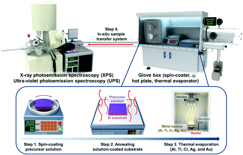 | ||
| Scheme 1 Schematic illustration for preparation and characterization process of metal/MAPbI3 thin films. | ||
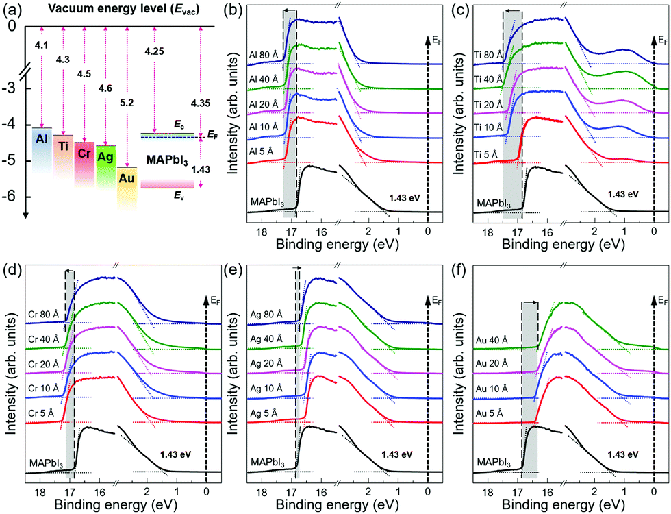 | ||
| Fig. 1 (a) Energy level scheme for isolated metals and MAPbI3 prior to interface formation used in this study. The work function is given for each material and the bandgap of MAPbI3 is included with 1.53 eV. Ec, Ev, and EF refer to the conduction, valence band, and the Fermi level, respectively. Thickness dependent UPS spectra of metal/MAPbI3 thin films showing the cutoff region and the VBM region. (b) Al/MAPbI3 thin films, (c) Ti/MAPbI3 thin films, (d) Cr/MAPbI3 thin films, (e) Ag/MAPbI3 thin films, and (f) Au/MAPbI3 thin films. The shaded areas and arrows in the spectra are guides to the eye and represent the shift of secondary cut off energy of MAPbI3 upon the metal deposition. | ||
Fig. 1b–f show the evolution of the UPS spectra at the secondary cutoff region and valence band region with the gradual deposition of various metal thin films. All the spectra were normalized to the same height. The secondary cut off energy was determined by linear extrapolation of the leading edge of the spectra.46 The shifts of secondary cut off energy are highlighted with shaded areas and arrows in the spectra. The vacuum level (VL) is obtained from the difference between the secondary cutoff energy and the photon energy (21.22 eV). For bare MAPbI3 thin films, it is found that the work function (WF) is 4.35 eV and the energy difference between the Fermi level and the valence band maximum (EF − EV) is 1.43 eV, comparable to those previously reported in literature.41,47 With a bandgap of 1.53 eV (Fig. S2, ESI†), the surface of MAPbI3 thin films studied in this work exhibits pronounced n-type character in agreement with previous reports.41,42,47 With the subsequent metal deposition of 5 Å, the VL of the metal/MAPbI3 thin films show an abrupt change. For Al, Ti, and Cr, the VL decreases to 3.99 eV, 4.23 eV, and 3.94 eV, whereas, for Ag and Au, the VL increases to 4.66 eV and 4.78 eV, respectively. As the thicknesses of the metal layers increase to 80 Å, the VL of metal/MAPbI3 saturate at 3.94 eV, 3.71 eV, 4.02 eV, 4.48 eV, and 4.90 eV for Al, Cr, Ti, Ag, and Au, respectively. The VL shift at the metal/MAPbI3 interfaces reveals that charge transfer occurs between the deposited metals and MAPbI3 thin films.48 Al, Ti, and Cr deposition on MAPbI3 leads downward VL shift, indicating that electrons are transferred from Al, Ti, and Cr to MAPbI3. On the other hand, the upward VL shift with Ag and Au deposition means electron transfer occurs from MAPbI3 thin films to the metal (Ag and Au). The valence band maximum (VBM) is determined by a linear extrapolation of valence band onset subtracted to the background around Fermi level.46 The valence band spectra show the similar trend with the evolution of secondary electron cut off with the increasing metal deposition (Fig. 1b–f and Fig S3 in ESI†). In addition, it can be seen that the metallic Fermi edge becomes pronounced and the perovskite-related features gradually attenuated with increasing metal thickness (Fig. S4, ESI†).
In order to further understand the energy level evolution and the interface reaction at the metal/MAPbI3 interfaces, we performed XPS analysis to investigate the chemical characteristics and the shift in the core-level spectra of MAPbI3 after the metal deposition (Fig. S5 and S6, ESI†). It can be known that the bare MAPbI3 and metal/MAPbI3 stacks remained free of contaminations during the whole experiment (Fig. S5, ESI†). Fig. 2 displays the evolution of the Pb 4f7/2 core level spectra as a function of the deposited metal thickness. The Pb 4f spectrum is attenuated at 80 Å Ti due to the limited probing depth of XPS. All the spectra were normalized to the same height to see changes in peak shapes and position clearly and the peak positions were obtained by Gaussian–Lorentzian fitting. For bare MAPbI3, the Pb 4f7/2 core level presents two peaks located at 138.24 eV and 136.74 eV (Fig. S7, ESI†). The larger Pb 4f7/2 peak is attributed to the Pb–I bonds in MAPbI3, while the smaller Pb 4f7/2 peak is a representative feature of metallic lead (Pb0).49,50 The formation of metallic Pb0 in the bare MAPbI3 is associated with losses of iodine atoms during sample annealing.47 After metal deposition, the Pb 4f7/2 core level clearly shifts toward lower binding energies. It is attributed to the formation of Pb0 at the metal/MAPbI3 interfaces, indicating redox reactions occur at the interface. The total shift of Pb 4f7/2 to lower binding energy is measured to be 0.2 ± 0.1 eV, indicating the upward band bending in MAPbI3 thin films induced by the metal deposition. Notably, it is evident that the metallic Pb0 peak (136.74 eV) becomes pronounced with increasing metal thickness. To evaluate the relative amount of Pb0, the evolution of the ratio of Pb2+ to Pb0 (Pb2+/Pb0) as a function of deposited metal thickness is plotted in Fig. 2f. For bare MAPbI3, the Pb2+/Pb0 is 27.77. The Pb2+/Pb0 is drastically decreased after 5 Å layer of metal deposition and saturates at 0.59 (Al), 0.98 (Ti), 1.07 (Cr), 4.21 (Ag), and 2.51 (Au) with increasing the deposited metal thickness, respectively. This trend indicates that Pb0 becomes enriched at the metal/MAPbI3 interface possibly due to charge transfer between the deposited metal layers and MAPbI3 thin films.
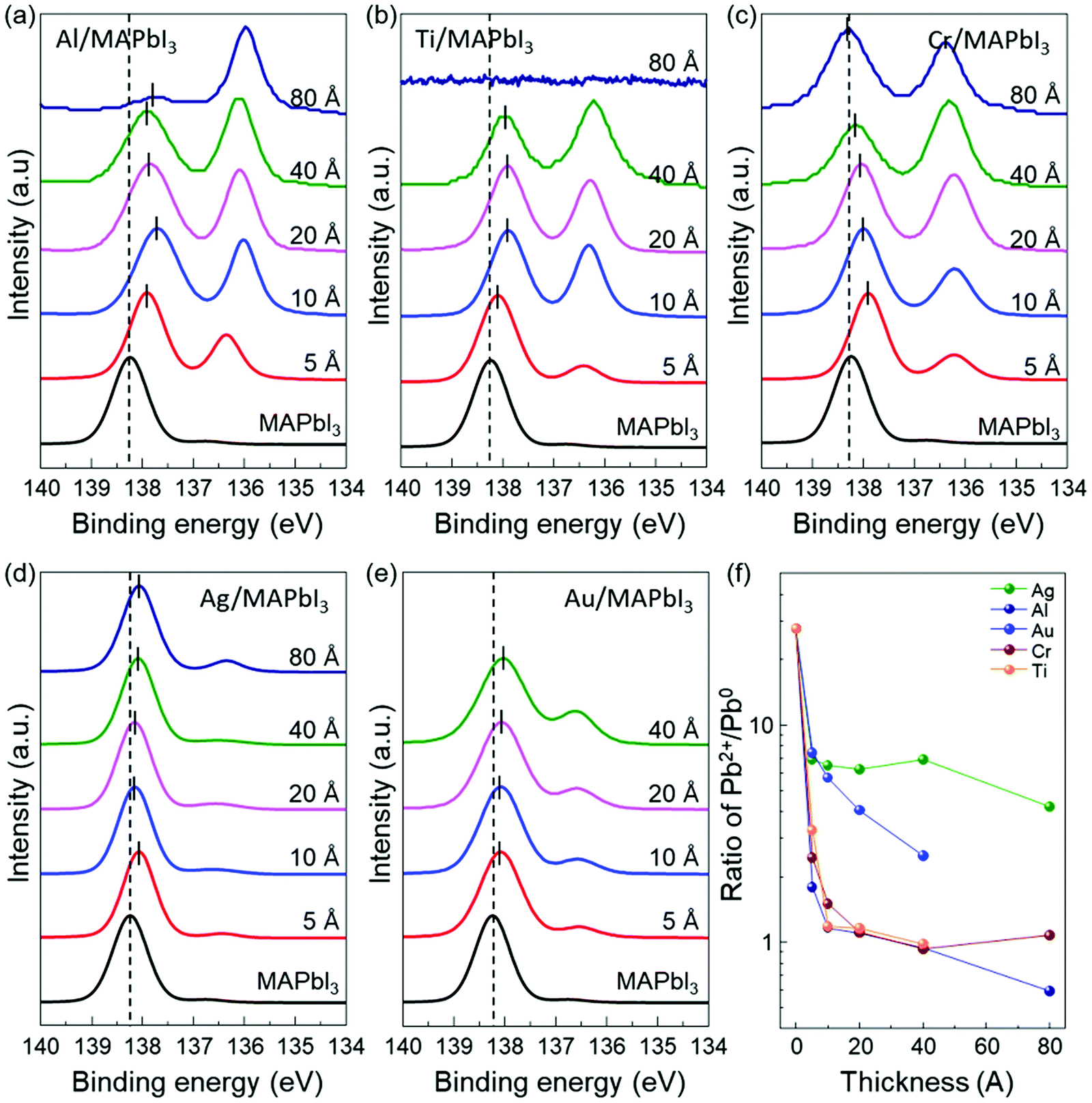 | ||
| Fig. 2 The evolution of Pb 4f7/2 XPS peaks of the metal/MAPbI3 thin films as a function of the deposited metal thickness. (a) Al/MAPbI3 thin films, (b) Ti/MAPbI3 thin films, (c) Cr/MAPbI3 thin films, (d) Ag/MAPbI3 thin films, and (e) Au/MAPbI3 thin films. The dashed lines mark the core levels Pb 4f7/2 of the pristine MAPbI3 thin films. (f) The ratio of Pb2+/Pb0 with increasing thickness of the deposited metal. | ||
To provide further information on the interaction between the deposited metal layers and the MAPbI3 thin films, we also obtained the Al 2p, Ti 2p, Cr 2p, Ag 3d and Au 4f core level spectra (Fig. 3). From the evolution of the metal core level spectra, it can be derived that the deposited metals were (partially) oxidized. It indicates that a redox reaction occurs at the metal/MAPbI3 interfaces resulting from the charge transfer between the deposited metal and MAPbI3 thin films. For example, we can find the dominant Al3+ (74.7 eV) and Ag+ (367.8 eV) peaks in Al 2p and Ag 3d5/2 spectra, which are associated to the Al and Ag component in aluminium halides and silver halides, respectively (Fig. 3a and d).51 The Au 4f7/2 spectra can be deconvoluted into two distinct components centered at 83.8 eV and 85.1 eV, which are ascribed to Au0 and Au +, respectively (Fig. 3e).52 The oxidized Al, Ag, or Au layers on MAPbI3 and the formation of Pb0 through reduction of Pb2+ suggest a redox reaction at Al/MAPbI3, Ag/MAPbI3, Au/MAPbI3 interfaces. In addition, it was observed that the peaks with higher binding energies, compare Al 2p, Ti 2p, and Cr 2p spectra in Fig. 3a–c, corresponding to higher oxidation states of the metals, are more dominant at low metal thickness (5 Å) as compared to 80 Å. With increasing metal layer thickness, the fraction of metallic component (Al0, Ti0, and Cr0) becomes stronger due to increasing contribution of neutral metals. The changes in the dominant oxidation states can be seen more clearly in metals with multivalent oxidation states, here for Ti and Cr.
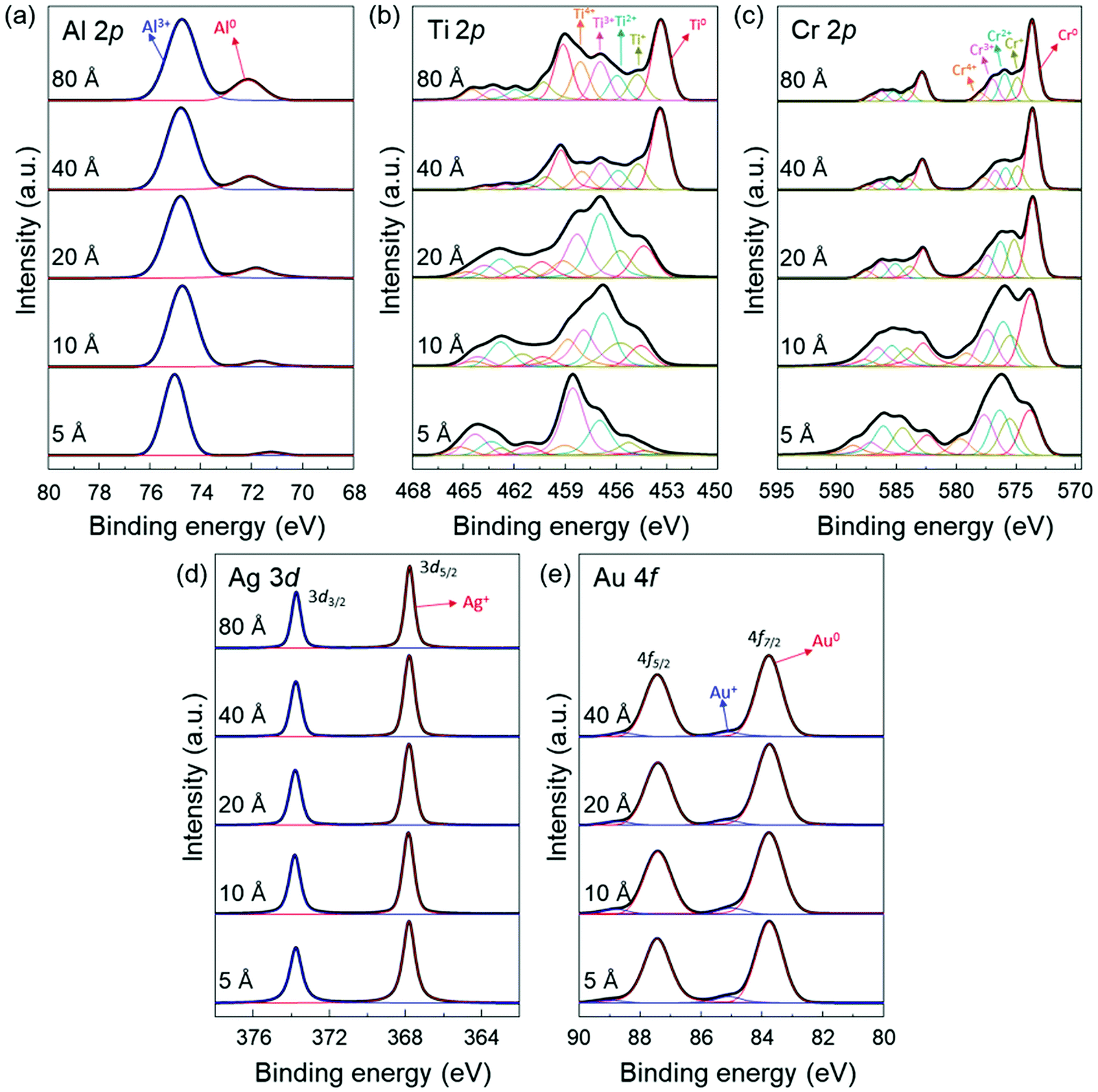 | ||
| Fig. 3 Thickness dependent XPS spectra of (a) the Al 2p peaks in the Al/MAPbI3 thin films, (b) the Ti 2p peaks in the Ti/MAPbI3 thin films, (c) the Cr 2p peaks in the Cr/MAPbI3 thin films, (d) the Ag 3d peaks in the Ag/MAPbI3 thin films, and (e) the Au 4f peaks in the Au/MAPbI3 thin films. | ||
The direct comparison of XPS spectra and their change with increasing metal layer thickness underline the redox reaction at the metal/MAPbI3 interface leading to the formation of metallic Pb. Previously, Liu et al. reported that no metallic Pb0 was observed at Au/MAPbI3 interfaces and this was explained by partial charge transfer in absence for evidence that would indicate a redox reaction.38 These differences are due to factors affecting the surface chemistry of halide perovskites, such as different synthesis methods, uncontrolled measurement conditions and degradation by air exposure or light illumination. Our findings indicate that the charge transfer leading to formation of Pb0 at the metal/MAPbI3 interfaces can be attributed to interface reactions between the deposited metal and halide perovskite, while the probability for MAPbI3 degradation driven by air, moisture, or light is relatively low given our experimental setup and not exposing the sample to air at any point.
To further investigate the underlying interfacial chemistries of the metal/MAPbI3 interfaces, time-of-flight secondary ion mass spectroscopy (ToF-SIMS) is employed to study the elemental distribution in the metal/MAPbI3 stacks. Fig. 4 shows the ToF-SIMS depth profiles of relative element distributions in Ag/MAPbI3, Au/MAPbI3, and Ti/MAPbI3 stacks. The boundaries of each layer were identified by the intensity of detected ions, as reported in previous studies.53,54 Al−, Au−, and Ti− ions are selected to identify the deposited metal layers, Pb− for Pb0 aggregates, PbI3− for the MAPbI3 thin films, Si− for the substrates. The maximum signals of AgI−, AuI−, and TiI− are observed at the Ag/MAPbI3, Au/MAPbI3, and Ti/MAPbI3 interfaces, indicating a chemical reaction between the deposited metals and iodine from the MAPbI3 surface. The formation of metal–iodine compounds is attributed to thermodynamically stronger bonds as compared to metal–metal bonds.43 In addition, the ToF-SIMS result of the bare MAPbI3 film (Fig. S8, ESI†) reveals that the concentration of Pb0 is higher in the bulk than at the surface, which is in good agreement with the Pb0 distribution in bare MAPbI3−xClx films reported by Sadoughi et al.50 However, the concentration of Pb0 at metal/MAPbI3 interfaces is comparable with that at bulk MAPbI3. It indicates that a substantial amount of Pb0 is existed at metal/MAPbI3 interfaces, consistent with XPS results.
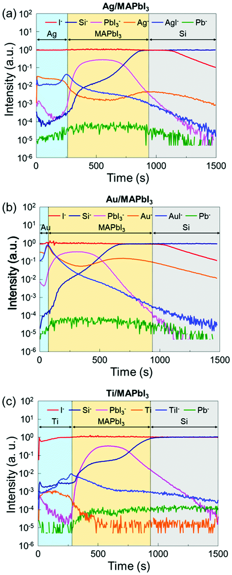 | ||
| Fig. 4 ToF-SIMS depth profiles of (a) the Ag/MAPbI3, (b) the Au/MAPbI3, and (c) the Ti/MAPbI3 stacks. | ||
Overall, our XPS and ToF-SIMS results provide evidence that the redox reaction between MAPbI3 and all investigated metals occurs. It has been reported that thermodynamically unfavorable reactions can occur at metal/semiconductor, especially metal/Pb(Zr,Ti)O3 interface, due to the heat of condensation of metal atoms.55–57 However, the formation of metal–iodine bond is thermodynamically favor due to the negative formation enthalpy and energy barrier,43 resulting in the formation of Pb0 state at metal/MAPbI3 interfaces (Table S1, ESI†). Generally, it is believed that Ag has higher reactivity with halide perovskite compared to other metals.28,58,59 The energy barrier for Ag and standard enthalpy of formation of AgI are less negative than those of Al, Cr and Ti. This trend is in good agreement with our experimental results. The difference between our results and the previous reports is attributed to the sample preparation and measurement methods. Our samples were investigated immediately after metal deposition without exposure to air and moisture, whereas the previous reports focused on the degradation mechanism of Ag/halide perovskite interfaces under air/humid conditions for more than several days. We speculate that the following reactions occur at the interface between MAPbI3 and the metal, M (with valency, z) account for the charge transfer of electrons due to the formation of the metal–iodine compounds which reduce Pb2+ in MAPbI3 to Pb0.
| M0 + zI− → MIz + ze− | (1) |
| Pb2+ + 2ze− → Pb0 | (2) |
It has been reported that Pb0 in pristine halide perovskites acts as a donor-like surface state, which pins EF at the surface.41,42 Thus we speculate that the Pb0 formed at the metal/MAPbI3 interface could influence the charge transport behavior. Next, we extract the effective Schottky barrier height (SBH) for electrons, which is one of the important parameters determining charge transfer efficiency, from the Pb 4f7/2 core level shifts in the metal/MAPbI3 interfaces using the following equation:60
| ϕB = Eg − Eiv + (Eicore − Emetalcore) = Eg − (Emetalcore − EVC) | (3) |
The extracted SBH values of the metal/MAPbI3 thin films are plotted as a function of the metal work function, as shown in Fig. 5a. The WF and SBH variations depending on the thickness of each metal appear as error bars in the x-axis and in the y-axis. It is apparent that the extracted SBHs are independent of metal work functions. To estimate the pinning factor (S) and charge neutrality level (ϕCNL), we perform a linear fit using the Schottky–Mott law and the Sze model.61 The details in the fitting method are described in ESI.† The value of S varies from 1 for ideal interface without Fermi-level pinning to 0 for a strongly pinned interface. The obtained S value for the metal/MAPbI3 interfaces is 0.06 when the thickness of the deposited metal layer is 40 Å and the ϕCNL is estimated to be 4.63 eV from the vacuum level, close to the Fermi level and above valence band maximum. This result reveals a strong Fermi-level pinning at the metal/MAPbI3 interface, therefore an ohmic contact cannot be formed between MAPbI3 and the metals investigated here (Fig. 5b).
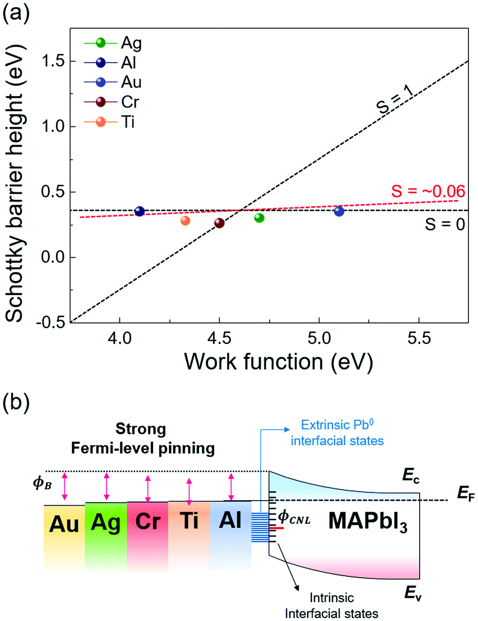 | ||
| Fig. 5 (a) Extracted Schottky barrier heights of MAPbI3 for the various metal work functions, showing the pinning factor S ∼ 0.06 when the deposited metal thickness is 40 Å (red dashed line). (b) Band diagram of metal/MAPbI3 interfaces with five different metals. | ||
We also calculated the density of the gap states (Dg) at the metal/MAPbI3 interfaces using the Sze model because the gap states is known to induce Fermi-level pinning at metal/semiconductor junctions (details are given in ESI†).61,62 The calculated gap Dg are the sum of the density metal-induced gap states (DMIGS) and interface trap states (DIT), the Dg, DMIGS, and DIT are estimated to be 2.09 × 10¹⁵, 4.16 × 10¹³, and 2.05 × 10¹⁵ eV−1 cm−2, respectively. This result indicates that the interface trap states mainly cause the strong Fermi-level pinning at metal/MAPbI3 interfaces. Strikingly, the density of calculated gap states at the metal/MAPbI3 interfaces is two orders of magnitude larger than the previously reported surface state density of bare MAPbI3 (∼1013 eV−1 cm−2).63 Probably, the formation of Pb0 due to the redox reaction between the deposited metal and iodine in MAPbI3 contributes to the difference in Dg. This result indicates that the metal/MAPbI3 interfaces suffer from low charge transfer efficiency due to the Pb0-interface trap state-induced strong Fermi-level pinning. Therefore, to enable efficient charge transport at the meal/MAPbI3 interfaces, the redox reaction resulting in the formation of extrinsic interface trap state should be suppressed.
Furthermore, our experimental ϕCNL of MAPbI3 is in agreement with the theoretical value of the Pb0-related defect energy levels of MAPbI3.64 It means that the Pb0 trap states at the metal/MAPbI3 interfaces can act as nonradiative recombination sites, resulting in performance degradation of halide perovskite-based devices.50 It has been reported that different surface termination leads to changes in Fermi-level pinning at the surface of pristine halide perovskite due to the different amount of surface states.63 However, it is uncertain that controlled surface termination of halide perovskite surface can suppress the reaction at the interface between the metal and halide perovskite. To reduce the Pb0-interface trap states at the metal/MAPbI3 thin films, an interlayer such as graphene and polymer thin films, which can prevent the reaction between the metal and halide perovskite, should be inserted at the interface.53,65
Conclusions
In summary, we have experimentally investigated the evolution of interfacial properties and Fermi-level pinning at the interface between MAPbI3 and Al, Ti, Cr, Ag, and Au. XPS measurements indicate accumulation of Pb0 at the metal/MAPbI3 interfaces with subsequently increasing metal layer thickness. The formation of Pb0 aggregates at the interfaces is attributed to the interfacial reaction between the deposited metal and iodine ion from MAPbI3, confirmed by ToF-SIMS analysis. Based on the core level shift in metal/MAPbI3 interfaces, we obtained the effective Schottky barrier heights and the pinning factor between the metals and MAPbI3. The pinning factor of MAPbI3 is 0.06, indicating that Schottky barrier heights at the metal/MAPbI3 interfaces are independent with metal work function. The charge neutrality level of MAPbI3 is 4.62 eV less than 0.3 eV from the EF, consistent with Pb0-related defects energy levels of MAPbI3. The Pb0 aggregates have a detrimental impact on efficient transport and transfer of electrons and photogenerated carriers at the metal/MAPbI3 interfaces, as they act as interface trap sites and nonradiative recombination sites. This research suggests that the electrical properties of metal/MAPbI3 interfaces are dominated by Pb0-related defects in MAPbI3, resulting from the interfacial reaction. It also indicates that control of chemical bonding states, especially metal–iodine reactivity, is a key engineering parameter for designing higher performance halide perovskite-based devices.Experimental section
Synthesis and sample preparation
CH3NH3PbI3 (MAPbI3) films were fabricated on p-type Si substrates using one-step spin coating method in a N2-filled glove box. The MAPbI3 precursor solution was prepared by MAI (≥99%, Sigma-Aldrich) and PbI2 (99.999% metal basis, Sigma-Aldrich) in molar ratio of 1![[thin space (1/6-em)]](https://www.rsc.org/images/entities/char_2009.gif) :1 in anhydrous N,N-dimethlyformamide (DMF) for overall concentration of 40 wt%. The mixed precursor solution was stirred for 24 h under 70 °C on a hot plate in a glove box. Before spin-coating of the MAPbI3 precursor solution, ultraviolet (UV)-O3 surface treatment was conducted on p-type Si substrates to make the surface of substrates hydrophilic to obtain a uniform and large-grain MAPbI3 film. The MAPbI3 precursor solution was spun onto the p-type Si substrate at a rate of 4000 rpm for 30 s. The films were annealed on a hot plate at 110 °C for 30 min. For metal deposition, the MAPbI3 films were loaded into an ultra-high vacuum thermal evaporation system, which are integrated with the glove box, and Ag, Al, Au, Cr and Ti were deposited on the MAPbI3 films with an equal deposition rate of 0.1 Å s−1. The base pressure of the thermal evaporator was maintained at 10−10 mbar and the pressure during metal deposition was less than 5 × 10⁻⁷ mbar. The thickness of evaporated metal films was monitored by a quartz crystal microbalance and was also confirmed by X-ray reflectivity measurements.
:1 in anhydrous N,N-dimethlyformamide (DMF) for overall concentration of 40 wt%. The mixed precursor solution was stirred for 24 h under 70 °C on a hot plate in a glove box. Before spin-coating of the MAPbI3 precursor solution, ultraviolet (UV)-O3 surface treatment was conducted on p-type Si substrates to make the surface of substrates hydrophilic to obtain a uniform and large-grain MAPbI3 film. The MAPbI3 precursor solution was spun onto the p-type Si substrate at a rate of 4000 rpm for 30 s. The films were annealed on a hot plate at 110 °C for 30 min. For metal deposition, the MAPbI3 films were loaded into an ultra-high vacuum thermal evaporation system, which are integrated with the glove box, and Ag, Al, Au, Cr and Ti were deposited on the MAPbI3 films with an equal deposition rate of 0.1 Å s−1. The base pressure of the thermal evaporator was maintained at 10−10 mbar and the pressure during metal deposition was less than 5 × 10⁻⁷ mbar. The thickness of evaporated metal films was monitored by a quartz crystal microbalance and was also confirmed by X-ray reflectivity measurements.
Metal/MAPbI3 interface characterization
The morphology and crystal structure of MAPbI3 thin films were characterized by scanning electron microscope (SU-70, Hitachi) and X-ray diffraction (D-8 Advance, Bruker Miller). The absorption spectra of MAPbI3 thin films on glass substrates were measured by an ultraviolet-visible photospectrometer (V-740, JASCO). To avoid air and moisture exposure and contamination, the prepared metal (Ag, Al, Au, Cr and Ti)/MAPbI3 thin film samples in glove box were transferred into ultrahigh vacuum chamber for UPS and XPS measurement system via a ultra-high vacuum tube (<10−8 mbar). The XPS, and UPS analyses were conducted using advanced in situ nanosurface analysis system (AISAS, KBSI, Korea). XPS was performed using an AXIS Ultra DLD model (KRATOS, U.K.) operating at a base pressure of 5 × 10⁻¹⁰ mbar at 300 K with a monochromatic Al Kα line at 1486.69 eV. UPS was performed using a He I (21.2 eV) source. The results were corrected for charging effects using Au 4f as an internal reference. The binding energies of all UPS and XPS spectra were calibrated and referenced to the Fermi level (EF) of the analyzer. A time-of-flight secondary ion mass spectroscopy (IONTOF, Germany) used for chemical depth profile of Ti/MAPbI3, Ag/MAPbI3, and Au/MAPbI3 interfaces with Cs+ primary ions (1 keV, 100 nA, 500 × 500 μm2) for the erosion and a Bi+ pulsed primary ion beam (30 keV, 1 pA, 100 × 100 μm2) for the analysis. Measurements were collected in non-interlaced mode to minimize beam damage from the primary beam.Conflicts of interest
The authors declare no competing financial interests.Acknowledgements
This work was financially supported by the Future Material Discovery (2016M3D1A1027666) Program, the Basic Research Laboratory (2018R1A4A1022647), and the National Research Foundation of Korea (NRF) grant funded by the Korean government MSIT (2019M3E6A1103818). K. S. C. acknowledges financial support from the Basic Science Research Program through the National Research Foundation of Korea funded by the Ministry of Science and ICT (NRF-2017M3A7B4049176). K. H. acknowledges Overseas Postdoctoral Fellowship of Basic Science Research Program through the National Research Foundation of Korea (NRF) funded by the Ministry of Education (2021R1A6A3A03039891). This material is based upon work performed by the Joint Center for Artificial Photosynthesis, a DOE Energy Innovation Hub, supported through the Office of Science of the U.S. Department of Energy under Award No. DE-SC0004993 (K. H. and C. M. S.-F.).References
- A. Kojima, K. Teshima, Y. Shirai and T. Miyasaka, J. Am. Chem. Soc., 2009, 131, 6050–6051 CrossRef CAS PubMed.
- H.-S. Kim, C.-R. Lee, J.-H. Im, K.-B. Lee, T. Moehl, A. Marchioro, S.-J. Moon, R. Humphry-Baker, J.-H. Yum, J. E. Moser, M. Grätzel and N.-G. Park, Sci. Rep., 2012, 2, 591 CrossRef PubMed.
- M. M. Lee, J. Teuscher, T. Miyasaka, T. N. Murakami and H. J. Snaith, Science, 2012, 338, 643–647 CrossRef CAS PubMed.
- N. J. Jeon, J. H. Noh, Y. C. Kim, W. S. Yang, S. Ryu and S. I. Seok, Nat. Mater., 2014, 13, 897–903 CrossRef CAS PubMed.
- D. P. McMeekin, G. Sadoughi, W. Rehman, G. E. Eperon, M. Saliba, M. T. Hörantner, A. Haghighirad, N. Sakai, L. Korte, B. Rech, M. B. Johnston, L. M. Herz and H. J. Snaith, Science, 2016, 351, 151–155 CrossRef CAS PubMed.
- H. Min, M. Kim, S.-U. Lee, H. Kim, G. Kim, K. Choi, J. H. Lee and S. I. Seok, Science, 2019, 366, 749–753 CrossRef CAS PubMed.
- NREL, N., Best Research-Cell Efficiency Chart, US Department of Energy, 2019.
- W.-J. Yin, T. Shi and Y. Yan, Adv. Mater., 2014, 26, 4653–4658 CrossRef CAS PubMed.
- S. De Wolf, J. Holovsky, S.-J. Moon, P. Löper, B. Niesen, M. Ledinsky, F.-J. Haug, J.-H. Yum and C. Ballif, J. Phys. Chem. Lett., 2014, 5, 1035–1039 CrossRef CAS PubMed.
- S. D. Stranks, G. E. Eperon, G. Grancini, C. Menelaou, M. J. P. Alcocer, T. Leijtens, L. M. Herz, A. Petrozza and H. J. Snaith, Science, 2013, 342, 341–344 CrossRef CAS PubMed.
- C. M. Sutter-Fella, Y. Li, M. Amani, J. W. Ager, F. M. Toma, E. Yablonovitch, I. D. Sharp and A. Javey, Nano Lett., 2016, 16, 800–806 CrossRef CAS PubMed.
- M. A. Green, Y. Jiang, A. M. Soufiani and A. Ho-Baillie, J. Phys. Chem. Lett., 2015, 6, 4774–4785 CrossRef CAS PubMed.
- J. Choi, J. S. Han, K. Hong, S. Y. Kim and H. W. Jang, Adv. Mater., 2018, 30, 1704002 CrossRef PubMed.
- J. H. Noh, S. H. Im, J. H. Heo, T. N. Mandal and S. I. Seok, Nano Lett., 2013, 13, 1764–1769 CrossRef CAS PubMed.
- D. M. Jang, K. Park, D. H. Kim, J. Park, F. Shojaei, H. S. Kang, J.-P. Ahn, J. W. Lee and J. K. Song, Nano Lett., 2015, 15, 5191–5199 CrossRef CAS PubMed.
- A. Younis, C.-H. Lin, X. Guan, S. Shahrokhi, C.-Y. Huang, Y. Wang, T. He, S. Singh, L. Hu, J. R. D. Retamal, J.-H. He and T. Wu, Adv. Mater., 2021, 2005000, DOI:10.1002/adma.202005000.
- Y.-H. Kim, H. Cho, J. H. Heo, T.-S. Kim, N. Myoung, C.-L. Lee, S. H. Im and T.-W. Lee, Adv. Mater., 2015, 27, 1248–1254 CrossRef CAS PubMed.
- J. Xing, X. F. Liu, Q. Zhang, S. T. Ha, Y. W. Yuan, C. Shen, T. C. Sum and Q. Xiong, Nano Lett., 2015, 15, 4571–4577 CrossRef CAS PubMed.
- K. C. Kwon, K. Hong, Q. V. Le, S. Y. Lee, J. Choi, K.-B. Kim, S. Y. Kim and H. W. Jang, Adv. Funct. Mater., 2016, 26, 4213–4222 CrossRef CAS.
- X. Y. Chin, D. Cortecchia, J. Yin, A. Bruno and C. Soci, Nat. Commun., 2015, 6, 7383 CrossRef CAS PubMed.
- J. Choi, S. Park, J. Lee, K. Hong, D.-H. Kim, C. W. Moon, G. D. Park, J. Suh, J. Hwang, S. Y. Kim, H. S. Jung, N.-G. Park, S. Han, K. T. Nam and H. W. Jang, Adv. Mater., 2016, 28, 6562–6567 CrossRef CAS PubMed.
- S. G. Kim, Q. V. Le, J. S. Han, H. Kim, M.-J. Choi, S. A. Lee, T. L. Kim, S. B. Kim, S. Y. Kim and H. W. Jang, Adv. Funct. Mater., 2019, 29, 1906686 CrossRef CAS.
- P. Schulz, D. Cahen and A. Kahn, Chem. Rev., 2019, 119, 3349–3417 CrossRef CAS PubMed.
- S. Wang, T. Sakurai, W. Wen and Y. Qi, Adv. Mater. Interfaces, 2018, 5, 1800260 CrossRef.
- M.-F. Lo, Z.-Q. Guan, T.-W. Ng, C.-Y. Chan and C.-S. Lee, Adv. Funct. Mater., 2015, 25, 1213–1218 CrossRef CAS.
- P. Schulz, L. L. Whittaker-Brooks, B. A. MacLeod, D. C. Olson, Y.-L. Loo and A. Kahn, Adv. Mater. Interfaces, 2015, 2, 1400532 CrossRef.
- P. Schulz, E. Edri, S. Kirmayer, G. Hodes, D. Cahen and A. Kahn, Energy Environ. Sci., 2014, 7, 1377–1381 RSC.
- Y. Kato, L. K. Ono, M. V. Lee, S. Wang, S. R. Raga and Y. Qi, Adv. Mater. Interfaces, 2015, 2, 1500195 CrossRef.
- J. Zhao, X. Zheng, Y. Deng, T. Li, Y. Shao, A. Gruverman, J. Shield and J. Huang, Energy Environ. Sci., 2016, 9, 3650–3656 RSC.
- L. Zhao, R. A. Kerner, Z. Xiao, Y. L. Lin, K. M. Lee, J. Schwartz and B. P. Rand, ACS Energy Lett., 2016, 1, 595–602 CrossRef CAS.
- J. Wang, J. Li, Y. Zhou, C. Yu, Y. Hua, Y. Yu, R. Li, X. Lin, R. Chen, H. Wu, H. Xia and H.-L. Wang, J. Am. Chem. Soc., 2021, 143, 7759–7768 CrossRef CAS PubMed.
- H. Kim, J. S. Han, J. Choi, S. Y. Kim and H. W. Jang, Small Methods, 2018, 2, 1700310 CrossRef.
- S. M. Sze and K. K. Ng, Physics of semiconductor devices, John Wiley & Sons, 2006 Search PubMed.
- Y. Hu, J. Zhou, P.-H. Yeh, Z. Li, T.-Y. Wei and Z. L. Wang, Adv. Mater., 2010, 22, 3327–3332 CrossRef CAS PubMed.
- W. A. Laban and L. Etgar, Energy Environ. Sci., 2013, 6, 3249–3253 RSC.
- W. Peng, L. Wang, B. Murali, K.-T. Ho, A. Bera, N. Cho, C.-F. Kang, V. M. Burlakov, J. Pan, L. Sinatra, C. Ma, W. Xu, D. Shi, E. Alarousu, A. Goriely, J.-H. He, O. F. Mohammed, T. Wu and O. M. Bakr, Adv. Mater., 2016, 28, 3383–3390 CrossRef CAS PubMed.
- C. Gu and J.-S. Lee, ACS Nano, 2016, 10, 5413–5418 CrossRef CAS PubMed.
- X. Liu, C. Wang, L. Lyu, C. Wang, Z. Xiao, C. Bi, J. Huang and Y. Gao, Phys. Chem. Chem. Phys., 2015, 17, 896–902 RSC.
- C.-H. Lin, T.-Y. Li, B. Cheng, C. Liu, C.-W. Yang, J.-J. Ke, T.-C. Wei, L.-J. Li, A. Fratalocchi and J.-H. He, Nano Energy, 2018, 53, 817–827 CrossRef CAS.
- J. Wang, S. P. Senanayak, J. Liu, Y. Hu, Y. Shi, Z. Li, C. Zhang, B. Yang, L. Jiang, D. Di, A. V. Ievlev, O. S. Ovchinnikova, T. Ding, H. Deng, L. Tang, Y. Guo, J. Wang, K. Xiao, D. Venkateshvaran, L. Jiang, D. Zhu and H. Sirringhaus, Adv. Mater., 2019, 31, 1902618 CrossRef PubMed.
- F. Zu, P. Amsalem, M. Ralaiarisoa, T. Schultz, R. Schlesinger and N. Koch, ACS Appl. Mater. Interfaces, 2017, 9, 41546–41552 CrossRef CAS PubMed.
- F.-S. Zu, P. Amsalem, I. Salzmann, R.-B. Wang, M. Ralaiarisoa, S. Kowarik, S. Duhm and N. Koch, Adv. Opt. Mater., 2017, 5, 1700139 CrossRef.
- W. M. Haynes, CRC handbook of chemistry and physics, CRC press, 2014 Search PubMed.
- X. Li, W. Li, Y. Yang, X. Lai, Q. Su, D. Wu, G. Li, K. Wang, S. Chen, X. W. Sun and A. K. K. Kyaw, Sol. RRL, 2019, 3, 1900029 CrossRef.
- Q. Wang, Y. Shao, Q. Dong, Z. Xiao, Y. Yuan and J. Huang, Energy Environ. Sci., 2014, 7, 2359–2365 RSC.
- Q. V. Le, M. Park, W. Sohn, H. W. Jang and S. Y. Kim, Adv. Electron. Mater., 2017, 3, 1600448 CrossRef.
- P. Liu, X. Liu, L. Lyu, H. Xie, H. Zhang, D. Niu, H. Huang, C. Bi, Z. Xiao, J. Huang and Y. Gao, Appl. Phys. Lett., 2015, 106, 193903 CrossRef.
- H. Ishii, K. Sugiyama, E. Ito and K. Seki, Adv. Mater., 1999, 11, 605–625 CrossRef CAS.
- L. Li, X. Liu, L. Lyu, R. Wu, P. Liu, Y. Zhang, Y. Zhao, H. Wang, D. Niu, J. Yang and Y. Gao, J. Phys. Chem. C, 2016, 120, 17863–17871 CrossRef CAS.
- G. Sadoughi, D. E. Starr, E. Handick, S. D. Stranks, M. Gorgoi, R. G. Wilks, M. Bär and H. J. Snaith, ACS Appl. Mater. Interfaces, 2015, 7, 13440–13444 CrossRef CAS PubMed.
- C. Wagner, W. Riggs, L. Davis, J. Moulder and G. Muilenberg, Handbook of X-ray Photoelectron Spectroscopy, PerkinElmer Corp. Eden Prairie, MN, 1979, 38 Search PubMed.
- Z. Huo, C.-k. Tsung, W. Huang, X. Zhang and P. Yang, Nano Lett., 2008, 8, 2041–2044 CrossRef CAS PubMed.
- J. S. Han, Q. V. Le, J. Choi, H. Kim, S. G. Kim, K. Hong, C. W. Moon, T. L. Kim, S. Y. Kim and H. W. Jang, ACS Appl. Mater. Interfaces, 2019, 11, 8155–8163 CrossRef CAS PubMed.
- R. K. Gunasekaran, D. Chinnadurai, A. R. Selvaraj, R. Rajendiran, K. Senthil and K. Prabakar, Chem. Phys. Chem., 2018, 19, 1507–1513 CrossRef CAS PubMed.
- L. J. Brillson, Phys. Rev. Lett., 1978, 40, 260 CrossRef CAS.
- F. Chen, R. Schafranek, W. Wu and A. Klein, J. Phys. D: Appl. Phys., 2011, 44, 255301 CrossRef.
- J. F. McGilp, J. Phys. C: Solid State Phys., 1984, 17, 2249 CrossRef CAS.
- W. Ming, D. Yang, T. Li, L. Zhang and M.-H. Du, Adv. Sci., 2018, 5, 1700662 CrossRef PubMed.
- J. T. Tisdale, E. Muckley, M. Ahmadi, T. Smith, C. Seal, E. Lukosi, I. N. Ivanov and B. Hu, Adv. Mater. Interfaces, 2018, 5, 1800476 CrossRef.
- K. M. Tracy, P. J. Hartlieb, S. Einfeldt, R. F. Davis, E. H. Hurt and R. J. Nemanich, J. Appl. Phys., 2003, 94, 3939–3948 CrossRef CAS.
- A. M. Cowley and S. M. Sze, J. Appl. Phys., 1965, 36, 3212–3220 CrossRef CAS.
- S. Gupta, P. P. Manik, R. K. Mishra, A. Nainani, M. C. Abraham and S. Lodha, J. Appl. Phys., 2013, 113, 234505 CrossRef.
- T. Gallet, D. Grabowski, T. Kirchartz and A. Redinger, Nanoscale, 2019, 11, 16828–16836 RSC.
- A. Buin, P. Pietsch, J. Xu, O. Voznyy, A. H. Ip, R. Comin and E. H. Sargent, Nano Lett., 2014, 14, 6281–6286 CrossRef CAS PubMed.
- H. H. Yoon, S. Jung, G. Choi, J. Kim, Y. Jeon, Y. S. Kim, H. Y. Jeong, K. Kim, S.-Y. Kwon and K. Park, Nano Lett., 2017, 17, 44–49 CrossRef CAS PubMed.
Footnotes |
| † Electronic supplementary information (ESI) available. See DOI: 10.1039/d1tc03370k |
| ‡ Present address: Center for convergence property measurement, Korea Research Institute of Standards & Science (KRISS), Daejeon 34113, Republic of Korea. |
| This journal is © The Royal Society of Chemistry 2021 |