
 Open Access Article
 This Open Access Article is licensed under a
 Creative Commons Attribution 3.0 Unported Licence
Thickness effect on the ferroelectric properties of La-doped HfO2 epitaxial films down to 4.5 nm†
Tingfeng
Song
a,
Romain
Bachelet
b,
Guillaume
Saint-Girons
 b,
Nico
Dix
a,
Ignasi
Fina
*a and
Florencio
Sánchez
*a
b,
Nico
Dix
a,
Ignasi
Fina
*a and
Florencio
Sánchez
*a
aInstitut de Ciència de Materials de Barcelona (ICMAB-CSIC), Campus UAB, Bellaterra 08193, Barcelona, Spain. E-mail: ifina@icmab.es; fsanchez@icmab.es
bUniv. Lyon, Ecole Centrale de Lyon, INSA Lyon, Université Claude Bernard Lyon 1, CPE Lyon, CNRS, Institut des Nanotechnologies de Lyon – INL, UMR5270, 69134 Ecully, France
First published on 20th July 2021
Abstract
Stabilization of the orthorhombic phase of HfO2 with La allows very high polarization and endurance to be achieved. However, these properties have not been confirmed yet in films having a thickness of less than 10 nm. We have grown (111)-oriented La (2 at%) doped epitaxial HfO2 films on SrTiO3(001) and Si(001) substrates, and report on the thickness dependence of their ferroelectric properties. Films of less than 7 nm thickness show a high remanent polarization of about 30 μC cm−2, slight wake-up, an endurance of at least 1010 cycles and a retention of more than 10 years, with the endurance and retention measured at the same poling voltage. La-doped HfO2 films even as thin as 4.5 nm also show robust ferroelectric properties.
1. Introduction
The existence of a ferroelectric phase in Si-doped HfO2 films was first reported in 2011 by Böscke et al.1 In the following years, ferroelectricity was observed in HfO2 films doped with other chemical elements, including Al, Ga, Co, Mg, Zr, In, Er, Y, Nd, Sm, Gd, La, Sr and Ba.2 The dopant content required to stabilize the ferroelectric phase depends on the atom. For example, in Si, Al or Y doped films the optimal doping content is less than 10 at% and the optimal doping content windows are narrow. Instead, for Zr doped films the optimal window is centered around 50 at% and it is wide.2 Naturally, the remanent polarization (Pr) also depends on the doping atom and content. Theoretical3 and experimental4 studies have shown that Pr is higher when HfO2 is doped with atoms having a large ionic radius such as Y, La or Sr.Among the large radius dopant atoms studied, La has enabled excellent ferroelectric properties.5–9 Kosadaev et al.6 reported La-doped HfO2 films with Pr above 13 μC cm−2 and a very high endurance (limited by fatigue) of up to 1010 cycles. Schroeder et al.7 reported a very high Pr above 27 μC cm−2 and a moderately high endurance of 107 cycles, without fatigue and with a low wake-up effect. Schenk et al.10 concluded that the high polarization of polycrystalline La:HfO2 films is due to the strong orientation of the [001] polar axis towards the normal in these films. However, La:HfO2 films with a very high polarization do not show good endurance,7 as often occurs in HfO2 films doped with other dopants due to the endurance–polarization dilemma.11 Doping Hf0.5Zr0.5O2 (HZO) films with La was effective to enhance the endurance without diminishing the polarization.12,13 Further optimization of La:HfO2 films could perhaps allow the desired combination of high polarization and high endurance. On the other hand, ferroelectricity with Pr around 9 μC cm−2 was reported in La:HfO2 films of up to 1 μm thickness.8 In contrast, to our knowledge, the ferroelectric properties of La:HfO2 films thinner than 10 nm have not been reported.
Recently, the ferroelectric phase was stabilized in epitaxial La-doped HfO2 films.14 Films of thickness t = 8, 12 and 16 nm were grown on different oxide monocrystalline substrates buffered with La0.67Sr0.33MnO3 (LSMO) electrodes. The t = 12 nm film on (001)-oriented SrTiO3 (STO) exhibited the best properties, with Pr = 16 μC cm−2 and an endurance (limited by fatigue) of 107 cycles, while the high leakage of the thinner film (t = 8 nm) did not allow the measurement of the ferroelectric properties. We report here on (111)-oriented epitaxial La:HfO2 films with thicknesses ranging from 4.5 to 17.5 nm and showing excellent ferroelectric properties, including polarization, endurance and retention, which have not yet been achieved in polycrystalline or epitaxial La:HfO2 films. Epitaxial films, enabling better control of microstructure and crystal orientation, can help to better understand the properties of ferroelectric HfO2.15–21 We show that films with a 6.9 nm thickness, deposited on LSMO/STO(001), have a high Pr of up to about 30 μC cm−2 with an endurance greater than 1010 cycles. Robust ferroelectricity is preserved in 4.5 nm films, with Pr above 25 μC cm−2 and an endurance of 109 cycles. We also show that epitaxial La:HfO2 films on buffered Si(001) wafers exhibit excellent ferroelectric properties: a film with t = 6.9 nm has Pr above 32 μC cm−2 and an endurance of more than 5 × 10⁹ cycles. All films show good extrapolated retention beyond 10 years.
2. Experimental
La:HfO2 films and bottom LSMO electrodes were grown via a single process by pulsed laser deposition using a KrF excimer laser. Sintered Hf0.98La0.02O2−x and La0.67Sr0.33MnO3 ceramics were used as targets. The LSMO electrodes were deposited at a substrate temperature Ts = 700 °C, an oxygen pressure of 0.1 mbar and a laser frequency of 5 Hz. The growth parameters for La:HfO2 films were 2 Hz of laser frequency, Ts = 800 °C and an oxygen pressure of 0.1 mbar. A series of La:HfO2 films with thickness t = 4.5, 6.9, 9.2 and 17.5 nm were grown on the LSMO electrodes (t = 25 nm) via a single process. STO(001) and STO buffered Si(001) were used as substrates in each deposition process. The STO buffer layers were grown ex situ by molecular beam epitaxy.22,23 Circular platinum top electrodes of a 20 μm diameter and a 20 nm thickness were deposited ex situ by sputtering on the La:HfO2 films through stencil masks for electrical measurements. Platinum top electrodes of a 14 μm diameter were additionally deposited on the t = 4.5 nm film on Si(001) to reduce the leakage effect on the measurement of polarization loops.The crystal structure was characterized by X-ray diffraction (XRD) with Cu Kα radiation using a Siemens D5000 and a Bruker D8-Discover diffractometer equipped with a point detector, and a Bruker D8-Advance diffractometer equipped with a 2D detector. The surface topography was studied by atomic force microscopy (AFM) using a Keysight 5100 in dynamic mode.
Ferroelectric polarization loops, leakage current, endurance and retention were measured at room temperature by using an AixACCT TFAnalyser2000 platform, and connecting the LSMO bottom electrode to the ground and biasing the top Pt contact. Ferroelectric polarization loops were obtained in dynamic leakage current compensation (DLCC) mode with a frequency of 1 kHz.24,25 Endurance was evaluated using bipolar square pulses, and after cycling the memory window was extracted by DLCC. Retention was measured by poling the sample using a triangular pulse of 0.25 ms and determining the Pr from the first polarization curve of the polarization loop measured at 1 kHz using the positive-up negative-down protocol after a delay time. Leakage current has been measured with an integration time of 2 s and averaging the data collected with increasing and decreasing voltage. Capacitance (C) loops were measured using an impedance analyzer (HP4192LF, Agilent Co.) operated with an excitation voltage of 0.3 V at 20 kHz. Relative dielectric permittivity (εr)–voltage loops were extracted from capacitance values using the C = ε0εrA/t relation, where A is the electrode area and t is the film thickness.
3. Results
Fig. 1a shows the XRD 2θ–χ maps of the films on STO(001), measured using a 2D detector. In addition to the high intensity (001) and (002) reflections of the STO substrate and LSMO electrode, there are intense spots corresponding to the La:HfO2 film in all samples despite their low thicknesses. The thinnest films, t = 4.5 and 6.9 nm, exhibit only a bright circular spot at χ = 0° and 2θ around 30°, the position of the orthorhombic o-(111) reflection. An elongated bright spot corresponding to the monoclinic m-(−111) reflection is also present in the thicker film (t = 17.5 nm). Furthermore, in the maps of the thicker films, very weak spots can be seen at the position of the m-{002} reflections. θ–2θ scans around the main reflections of the La:HfO2 film, measured with a point detector, are presented in Fig. 1b. The o-(111) peak becomes narrower with increasing film thickness due to the size effect and is accompanied by Laue oscillations. The m-(−111) peak at 2θ ∼28.5° is clear in the t = 17.5 nm film, but not in the thinner ones. The XRD 2θ–χ maps and θ–2θ scans of the equivalent series of La:HfO2 films on Si(001) (Fig. S1, ESI†) confirm the presence of the orthorhombic phase in the entire thickness range and the appearance of the monoclinic phase in the thicker films, without substantial differences from the films on STO(001). The out-of-plane lattice parameter associated with the o-(111) reflection, do-(111), was determined from the position of the corresponding diffraction peak in the θ–2θ scans (Fig. 1c). The do-(111) value of the t = 4.5 nm film on STO(001) is close to 3.0 Å and decreases with increasing thickness to less than 2.98 Å in films thicker than about 10 nm. The films on Si(001) show a similar thickness dependence, but with smaller lattice parameters (do-(111) in the 2.95–2.96 Å range). The lower do-(111) of the La:HfO2 films on Si(001) is due to the low coefficient of thermal expansion of Si(001), which causes tensile stress in the films when cooled after growth.26,27 The do-(111) parameters of equivalent La-doped (1 at%) Hf0.5Zr0.49O2 films13 are also shown in Fig. 1c. The substrate and thickness dependences are coincident, but the do-(111) parameters of the La:HfO2 films are slightly expanded. The in-plane lattice distance along the [11−2] and HfO2[1−10] parameters of the t = 4.5, 6.9 and 9.2 nm films on STO(001) were determined by reciprocal space maps (Fig. S2, ESI†). The lattice distances are similar in the three films and close to the estimated values in relaxed undoped HfO2.28 Therefore, the thinner film shows a slight expansion of the out-of-plane parameter, while the in-plane parameters are basically relaxed. The pole figures around the o-(−111) reflections of La:HfO2 and (111) of STO (Fig. 1d) of the t = 17.5 nm film on STO(001) confirm the epitaxy of the orthorhombic phase. The twelve o(−111) poles indicate the presence of four in-plane crystal variants of o-HfO2. The epitaxial relationships with the STO substrate are [1−10]o-HfO2(111)//[1−10]STO(001) and [11−2]o-HfO2(111)//[1−10]STO(001). Additional information of the epitaxy of doped HfO2 on LSMO/STO(001) is reported elsewhere.29,30 | ||
| Fig. 1 XRD measurements of the La:HfO2 films on STO(001): (a) XRD 2θ–χ maps obtained with a 2D detector. The χ range is from −10° to +10°. (b) XRD θ–2θ scans obtained with a point detector. (c) Out-of-plane lattice distance, do-(111) (black circles). The red circles are the do-(111) values of the La:HfO2 films on Si(001), determined from the θ–2θ scans shown in Fig. S1, ESI.† Blue and green triangles represent the do-(111) values of epitaxial La-doped (1 at%) Hf0.5Zr0.49O2 films on STO(001) and Si(001), respectively.26 (d) Pole figures around o(−111) and STO(111) reflections of the t = 17.5 nm film on STO(001). | ||
The AFM topographic images (Fig. 2) of the La:HfO2 films on STO(001) show extremely flat surfaces. The morphology of terraces and steps presented by the STO substrates31 is replicated in the deposited LSMO and La:HfO2 films. The terraces in the films are well-visible, and the root mean square roughness, calculated in 5 μm × 5 μm areas, is 2.8 Å in the t = 17.5 nm film and less than 2 Å in the thinner films.
 | ||
| Fig. 2 Topographic AFM images (5 μm × 5 μm) of La:HfO2 films on STO(001) with a thickness of (a) 4.5 nm, (b) 6.9 nm, (c) 9.2 nm, and (d) 17.5 nm. Insets: 1 μm × 1 μm topographic images. | ||
The ferroelectric polarization loops of the La:HfO2 films on STO(001), measured using a high maximum applied field, are shown in Fig. 3a. The maximum electric field applied to measure the loops was lower in the thicker films, since the coercive electric field EC and the breakdown electric field decrease with the thickness. The two thinner films have a very high polarization, with Pr around 26 and 32 μC cm−2 in the t = 4.5 nm and t = 6.9 nm films, respectively. The polarization is decreases with increasing thickness, with Pr around 10 μC cm−2 in the t = 17.5 nm film. The t = 6.9 nm La:HfO2 film on Si(001) has the largest Pr of about 32 μC cm−2 (Fig. 3b). Note that the round shape of the loops near the maximum applied electric field is a signature of the residual leakage contribution, which results in a possible overestimation of the remanent polarization within 2 μC cm−2.32 All the loops shown in Fig. 3 have been collected at the largest applied electric field before breakdown, at saturation and after cycling the sample 10 times to avoid the wake-up effect discussed as follows and obtain comparable results. The dependences of Pr on the thickness of the La:HfO2 films on STO(001) and Si(001) are presented in Fig. 3c. Both series exhibit a similar thickness dependence, with the maximum Pr in the t = 6.9 nm films. The Pr of the La:HfO2 films ranges from 10 to 30 μC cm−2 on STO(001) and from 12 to 32.5 μC cm−2 on Si(001). We reported a similar Pr dependence for HZO33 and La-doped HZO13 films on STO(001). In contrast, epitaxial HZO34 and La-doped HZO13 films on Si(001) did not exhibit a peak and films thinner than 5 nm had the highest Pr. The dependence of the coercive electric field with thickness is shown in Fig. 3d. The EC of the films on both STO(001) and Si(001) decreases linearly with the thickness (in the logarithmic scale), with a slope of about 0.5. Thus, it follows approximately the EC ∝ t−2/3 dependence usually observed in high-quality ferroelectric perovskite films35–37 and epitaxial HfO2-based films,13,15,33,34 but scarcely observed in polycrystalline HfO2-based films.38
 | ||
| Fig. 3 Polarization loops of the films on STO(001) (a) and Si(001) (b). Dependence on the thickness of the remanent polarization (c) and the coercive electric field (d) of the films on STO(001) (black squares) and Si(001) (red circles). | ||
The films exhibit a small wake-up effect, basically observed only in the first cycle and when the applied maximum voltage was lower than that used to obtain fully saturated loops (Fig. 4). The wake-up is evidenced by a double peak in the current–voltage curves, causing a slight shrinkage in the polarization loop. Redistribution of oxygen vacancies or phase transitions induced by an electric field have been proposed as wake-up mechanisms.11 The wake-up effect in our epitaxial films is more pronounced if the maximum applied electric field is reduced (Fig. S3, ESI†). The minimal wake-up effect is in sharp contrast with the persistent wake-up effects commonly observed in polycrystalline La:HfO2 films,5–7 which were explained by the displacement of oxygen vacancies that induce the transformation from the monoclinic phase to the orthorhombic phase.7 However, the wake-up effect is usually null in epitaxial doped HfO2 films, even in epitaxial HZO films on STO(001) that have a significant amount of monoclinic phase. See the recent review of Fina and Sánchez15 for a description of the wake-up effects in epitaxial HfO2 films and the differences with polycrystalline HfO2 films. Some specific properties of epitaxial films can be responsible for the generally negligible wake-up effect compared to polycrystalline films: (i) use of electrodes (LSMO and Pt) more stable against oxidation, (ii) a lower number of defects in optimized epitaxial films, and (iii) a semi-coherent interface between the bottom electrode and the epitaxial HfO2 film. The fact that the here-reported La:HfO2 films show a more pronounced wake-up effect can be related to the larger number of defects compared with Zr doped films as a consequence of the larger dopant radii. In the case of epitaxial La:HfO2 films on Si(001), the wake-up effect is similar and also limited to a few cycles (Fig. S4, ESI†). Note also that the residual leakage contribution, signalled by a current increase near the maximum applied voltage and more prominent in thinner films, also reduces during cycling. This is in agreement with the oxygen vacancy redistribution upon cycling scenario proposed in polycrystalline films, although here the effects are minimal, indicating that the oxygen vacancy number is smaller in epitaxial films.
 | ||
| Fig. 4 Evolution with the number of cycles of current–voltage curves and the corresponding polarization loops of films on STO(001) with a thickness of (a) 4.5 nm, (b) 6.9 nm, (c) 9.2 nm, and (d) 17.5 nm. | ||
The leakage current curves of the films on STO(001) are shown in Fig. 5a. The leakage of the t = 4.5 nm film (3 × 10⁻⁶ A cm−2 at 1 MV cm−1) is moderately low considering the ultra-low thickness. The leakage of the thicker film, t = 17.5 nm, ranges from around 5 × 10⁻⁸ A cm−2 at a low field up to about 4 × 10⁻⁷ A cm−2 at 2 MV cm−1. The t = 6.9 nm film is highly insulating, with a leakage well below 10−8 A cm−2 at a low field and less than 5 × 10⁻⁸ A cm−2 at 1 MV cm−1. Therefore, the t = 6.9 nm film combines a very high Pr of about 30 μC cm−2 and a very low conductivity. The films on buffered Si(001) show more leakage, and only the t = 17.5 nm film exhibits a low leakage of less than 10−7 A cm−2 at 1 MV cm−1 (Fig. S5, ESI†). The dielectric permittivity loops of the films on STO(001) (Fig. 5b) vary greatly with the thickness of the films. The loop corresponding to the t = 4.5 nm film has a well-defined butterfly shape. The hysteresis reduces with increasing thickness, and it is barely appreciated in the t = 17.5 nm film. The value of the dielectric constant also depends on the thickness. The permittivity at a high electric field is ∼30 in the t = 4.5 and 6.9 nm films, and it is reduced to ∼28 in the t = 9.2 nm film and to ∼24.5 in the t = 17.5 nm film. The decrease of the dielectric constant is in agreement with the observation by XRD of an increase of the monoclinic phase fraction with thickness, and with the reported dependences of the permittivity of other doped HfO2 films on the ratio between orthorhombic and monoclinic phases.34,39–41
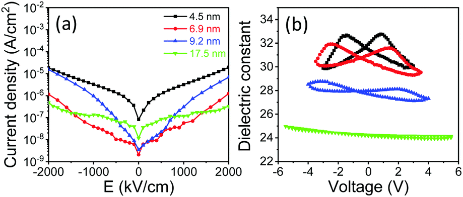 | ||
| Fig. 5 Leakage current curves (a) and dielectric constant loops (b) of the films on STO(001). | ||
The endurance of the films on STO(001) is shown in Fig. 6a–d. The polarization of the t = 4.5 nm film (Fig. 6a), cycled by electric pulses of amplitude 6.7 MV cm−1, increases from 2Pr = 19.5 μC cm−2 in the pristine state to 24.5 μC cm−2 after a few (less than ten) cycles, evidencing the small wake-up effect described above. With additional cycles the capacitor is fatigued and 2Pr decreases to 18.8 μC cm−2 after 105 cycles and then more abruptly to 6 μC cm−2 after 109 cycles. The loss of polarization is, on average, about 75% after eight magnitudes. The t = 6.9 nm film exhibits a similar behavior when cycled at 5.8 MV cm−1, 2Pr being 2.8 μC cm−2 after 1010 cycles (Fig. 6b). The polarization was higher for applied pulses of 6.5 MV cm−1, and 2Pr was 4 μC cm−2 when the measurement was stopped after 1010 cycles. A higher cycling electric field, 7.2 MV cm−1, causes a larger switchable polarization, but the capacitor undergoes hard breakdown after 109 cycles (open blue triangle in Fig. 6b). Representative polarization loops of the t = 6.9 nm film, measured applying several maximum electric fields and a number of cycles, are shown in Fig. S6, ESI.† The endurance of the t = 9.2 nm film (Fig. 6c) is similar, while it is highly degraded in the t = 17.5 nm film (Fig. 6d). This degradation is because hard breakdown occurs at a lower field as the film is thicker, which limits the applied field that can be applied. Breakdown occurs through conductive filaments formed after high enough electrical stress.42 Ionic conduction through incoherent boundaries between monoclinic and orthorhombic grains, more abundant in thicker films, can be a relevant contribution.43 Thus, there is not a direct relation with the thickness dependence of the current leakage (Fig. 5). A similar degradation of endurance with thickness has been observed in other epitaxial13,34 and polycrystalline44 doped-HfO2 films.
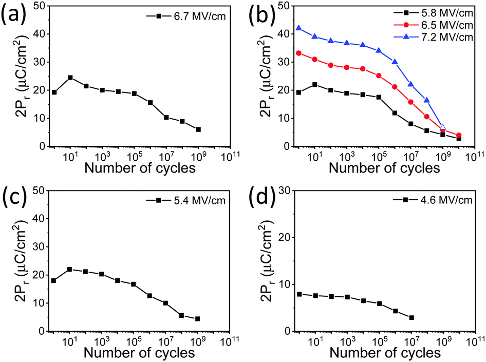 | ||
| Fig. 6 Endurance measurements of the films on STO(001) with a thickness of (a) 4.5 nm, (b) 6.9 nm, (c) 9.2 nm, and (d) 17.5 nm. The electric field of the cycles is indicated in the top right of each panel. | ||
Li et al. reported an endurance of up to 107 cycles in epitaxial La-doped (5.5 cat%) HfO2 films.14 The endurance was limited by fatigue, and they found that the loss of polarization was much more severe when the electrical stress was lower (lower pulse amplitude or shorter pulse width) and also when the interval between pulses was longer. It was argued that the high density of charged domain walls in incompletely switched capacitors could be pinned and then cause fatigue. In the case of polycrystalline doped HfO2 films, increased fatigue with decreasing electric field has been reported,45–47 as well as with increasing cycling frequency.46 Schroeder and coworkers46 proposed that the faster degradation of polarization by cycling with pulses of lower amplitudes or higher frequencies was caused by the less saturated switching in these cases (the frequency effect was due to the fact that the coercive field increases with the frequency). The fatigue mechanism suggested by Schroeder and coworkers46 considered that oxygen vacancies migrate during each cycle from switchable regions to non-switchable regions, creating local fields. The intensity of the local field strength would increase with cycling until the domains of the initially switchable regions would be pinned. On the other hand, Starschich et al.48 observed that hard breakdown occurred earlier, as the cycling frequency was lower, and they assumed that this was due to the suppression of generation of oxygen vacancies at high frequencies. In our epitaxial films, the amplitude of the electric field has a critical effect on the capacitor breakdown if it is too high. However, the amplitude of the electric field has no impact on the fatigue (Fig. S7, ESI†). It determines the fraction of ferroelectric domains that are switched and thus influences the polarization, but not the reduction of the normalized polarization with the number of cycles. On the other hand, the endurance of our films is also degraded by a lower cycling frequency, which causes here more fatigue or even breakdown (Fig. S8, ESI†). Note that low frequency measurements we performed implied long period pulses. Using the data shown in Fig. S7 (ESI†) as an example, a capacitor cycled N times by bipolar pulses of 3 V at 10 kHz is poled for a total time 100 times longer than another one cycled at 1 MHz. Therefore, the degradation effects induced by the applied field scale exponentially with the decrease of frequency (longer pulse duration and longer time between pulses), as expected in the redistribution of defects in the bulk of the device.49 Besides, a longer pulse also promotes the migration of free carriers towards domain walls, thus inducing a severer pinning effect.45
The retention of the films on STO(001) is shown in Fig. 7, where the remanent polarization is plotted as a function of the delay time after poling (td). Each film was poled at the same electric field used in the endurance measurements (Fig. 6), and for positive (blue squares) and negative (red circles) poling fields. The experimental data are fitted (blue and red dashed lines) to the rational dependence Pr = P0⋅t−nd.50 The vertical black dashed line corresponds to a time of 10 years. The extrapolated data indicate that the four films retain a high fraction of the initial polarization. The memory window (2Pr) extrapolated to 10 years of the thicker film, which has a high amount of paraelectric monoclinic phase, is 54% of the initial value. The percentage of the initial memory window of the thinnest film, t = 4.5 nm, is 53% despite the expected high depolarization fields. The t = 6.9 and 9.2 nm films maintain 69 and 63% of the initial memory window, respectively. Therefore, all films exhibit excellent retention after being poled with the same electric field used to determine the endurance properties. The retention of more than 10 years is accompanied by an endurance of at least 109 cycles in the t = 4.5 nm film and 1010 cycles in the t = 6.9 nm film. The equivalent t = 6.9 nm film on Si(001) also exhibits an endurance of at least 5 × 10⁹ cycles and a retention of more than 10 years (Fig. S9, ESI†).
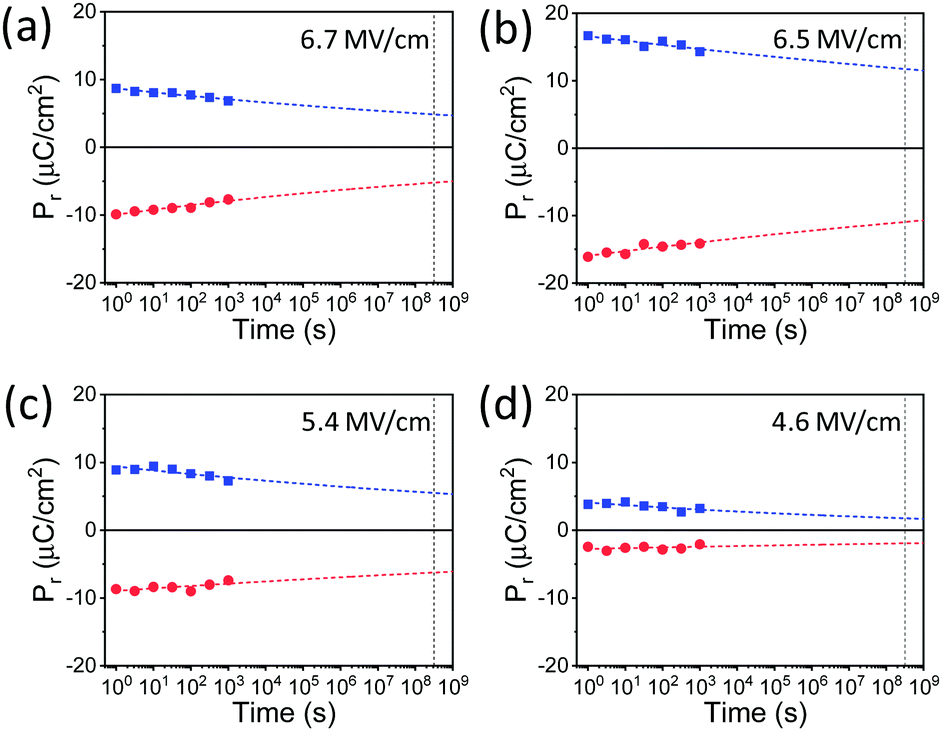 | ||
| Fig. 7 Retention measurements of the films on STO(001) with a thickness of (a) 4.5 nm, (b) 6.9 nm, (c) 9.2 nm, and (d) 17.5 nm. The electric field of the cycles is indicated in the top right of each panel. | ||
4. Conclusions
In summary, the orthorhombic phase of HfO2 has been epitaxially stabilized in La-doped films. The films present a majority of the orthorhombic phase, (111)-oriented, with an increased fraction of monoclinic phase in films thicker than 10 nm. The robust ferroelectric properties of La-doped HfO2 are preserved in films even as thin as 4.5 nm. The films exhibit minimal wake-up, basically limited to the first cycle. Films with a thickness less than 7 nm show a remanent polarization of about 30 μC cm−2, an endurance of 1010 cycles, and a retention of more than 10 years. These excellent properties are achieved in films epitaxially grown on either SrTiO3(001) or buffered Si(001) substrates.Conflicts of interest
There are no conflicts to declare.Acknowledgements
Financial support from the Spanish Ministry of Science and Innovation through the Severo Ochoa FUNFUTURE (CEX2019-000917-S), MAT2017-85232-R (AEI/FEDER, EU), PID2020-112548RB-I00 (AEI/FEDER, EU), and PID2019-107727RB-I00 (AEI/FEDER, EU) projects, from CSIC through the i-LINK (LINKA20338) program, and from Generalitat de Catalunya (2017 SGR 1377) is acknowledged. This study was supported by a 2020 Leonardo Grant for Researchers and Cultural Creators, BBVA Foundation. IF acknowledges Ramón y Cajal contract RYC-2017-22531. TS was financially supported by China Scholarship Council (CSC), grant no. 201807000104. TS's work has been done as a part of his PhD program in Materials Science at Universitat Autònoma de Barcelona. RB and GSG acknowledge the financial support from the European Commission through the project TIPS (No. H2020-ICT-02-2014-1-644453), from the French National Research Agency (ANR) through the projects DIAMWAFEL (No. ANR-15-CE08-0034) and MITO (No. ANR-17-CE05-0018), and from CNRS through the MITI interdisciplinary programs (project NOTE). They are also grateful to the joint laboratory INL-RIBER, P. Regreny, C. Botella and J. B. Goure for the MBE technical support on the Nanolyon technological platform.References
- T. S. Böscke, J. Müller, D. Bräuhaus, U. Schröder and U. Böttger, Appl. Phys. Lett., 2011, 99, 102903 CrossRef.
- U. Schröder, C. S. Hwang and H. Funakubo, Ferroelectricity in Doped Hafnium Oxide: Materials, Properties and Devices, Woodhead Publishing, 2019 Search PubMed.
- R. Batra, T. D. Huan, G. A. Rossetti and R. Ramprasad, Chem. Mater., 2017, 29, 9102 CrossRef CAS.
- S. Starschich and U. Boettger, J. Mater. Chem. C, 2017, 5, 333 RSC.
- A. G. Chernikova, D. S. Kuzmichev, D. V. Negrov, M. G. Kozodaev, S. N. Polyakov and A. M. Markeev, Appl. Phys. Lett., 2016, 108, 242905 CrossRef.
- M. G. Kozodaev, A. G. Chernikova, E. V. Korostylev, M. H. Park, U. Schroeder, C. S. Hwang and A. M. Markeev, Appl. Phys. Lett., 2017, 111, 132903 CrossRef.
- U. Schroeder, C. Richter, M. H. Park, T. Schenk, M. Pešić, M. Hoffmann, F. P. G. Fengler, D. Pohl, B. Rellinghaus, C. Zhou, C. C. Chung, J. L. Jones and T. Mikolajick, Inorg. Chem., 2018, 57, 2752 CrossRef CAS.
- T. Schenk, N. Godard, A. Mahjoub, S. Girod, A. Matavz, V. Bobnar, E. Defay and S. Glinsek, Phys. Status Solidi RRL, 2020, 14, 1900626 CrossRef CAS.
- C. Mart, K. Kühnel, T. Kämpfe, S. Zybell and W. Weinreich, Appl. Phys. Lett., 2019, 114, 102903 CrossRef.
- T. Schenk, C. M. Fancher, M. H. Park, C. Richter, C. Künneth, A. Kersch, J. L. Jones, T. Mikolajick and U. Schroeder, Adv. Electron. Mater., 2019, 5, 1900303 CrossRef CAS.
- M. H. Park, Y. H. Lee, T. Mikolajick, U. Schroeder and C. S. Hwang, MRS Commun., 2018, 8, 795 CrossRef CAS.
- M. G. Kozodaev, A. G. Chernikova, E. V. Korostylev, M. H. Park, R. R. Khakimov, C. S. Hwang and A. M. Markeev, J. Appl. Phys., 2019, 125, 034101 CrossRef.
- T. Song, R. Bachelet, G. Saint-Girons, R. Solanas, I. Fina and F. Sánchez, ACS Appl. Electron. Mater., 2020, 2, 3221 CrossRef CAS.
- X. Li, C. Li, Z. Xu, Y. Li, Y. Yang, H. Hu, Z. Jiang, J. Wang, J. Ren, C. Zheng, C. Lu and Z. Wen, Phys. Status Solidi RRL, 2021, 15, 2000481 CrossRef CAS.
- I. Fina and F. Sánchez, ACS Appl. Electron. Mater., 2021, 3, 1530 CrossRef CAS.
- J. Cao, S. Shi, Y. Zhu and J. Chen, Phys. Status Solidi RRL, 2021, 15, 2100025 CrossRef CAS.
- Z. Zhang, S. Hsu, V. A. Stoica, H. Paik, E. Parsonnet, A. Qualls, J. Wang, L. Xie, M. Kumari, S. Das, Z. Leng, M. McBriarty, R. Proksch, A. Gruverman, D. G. Schlom, L. Chen, S. Salahuddin, L. W. Martin and R. Ramesh, Adv. Mater., 2021, 33, 2006089 CrossRef CAS PubMed.
- Y. Wei, P. Nukala, M. Salverda, S. Matzen, H. J. Zhao, J. Momand, A. S. Everhardt, G. Agnus, G. R. Blake, P. Lecoeur, B. J. Kooi, J. Íñiguez, B. Dkhil and B. Noheda, Nat. Mater., 2018, 17, 1095 CrossRef CAS PubMed.
- H. Y. Yoong, H. Wu, J. Zhao, H. Wang, R. Guo, J. Xiao, B. Zhang, P. Yang, S. J. Pennycook, N. Deng, X. Yan and J. Chen, Adv. Funct. Mater., 2018, 28, 1806037 CrossRef.
- J. Lyu, I. Fina, R. Solanas, J. Fontcuberta and F. Sánchez, Appl. Phys. Lett., 2018, 113, 082902 CrossRef.
- T. Shimizu, K. Katayama, T. Kiguchi, A. Akama, T. J. Konno, O. Sakata and H. Funakubo, Sci. Rep., 2016, 6, 32931 CrossRef CAS PubMed.
- G. Saint-Girons, R. Bachelet, R. Moalla, B. Meunier, L. Louahadj, B. Canut, A. Carretero-Genevrier, J. Gazquez, P. Regreny, C. Botella, J. Penuelas, M. G. Silly, F. Sirotti and G. Grenet, Chem. Mater., 2016, 28, 5347 CrossRef CAS.
- J. Lyu, I. Fina, R. Bachelet, G. Saint-Girons, S. Estandía, J. Gázquez, J. Fontcuberta and F. Sánchez, Appl. Phys. Lett., 2019, 114, 222901 CrossRef.
- I. Fina, L. Fàbrega, E. Langenberg, X. Martí, F. Sánchez, M. Varela and J. Fontcuberta, J. Appl. Phys., 2011, 109, 074105 CrossRef.
- R. Meyer, R. Waser, K. Prume, T. Schmitz and S. Tiedke, Appl. Phys. Lett., 2005, 86, 142907 CrossRef.
- T. Song, H. Tan, N. Dix, R. Moalla, J. Lyu, G. Saint-Girons, R. Bachelet, F. Sánchez and I. Fina, ACS Appl. Electron. Mater., 2021, 3, 2106 CrossRef CAS.
- R. Moalla, B. Vilquin, G. Saint-Girons, G. Sebald, N. Baboux and R. Bachelet, CrystEngComm, 2016, 18, 1887 RSC.
- L. L. Tao, T. R. Paudel, A. A. Kovalev and E. Y. Tsymbal, Phys. Rev. B, 2017, 95, 245141 CrossRef.
- S. Estandía, N. Dix, J. Gazquez, I. Fina, J. Lyu, M. F. Chisholm, J. Fontcuberta and F. Sánchez, ACS Appl. Electron. Mater., 2019, 1, 1449 CrossRef.
- S. Estandía, N. Dix, M. F. Chisholm, I. Fina and F. Sánchez, Cryst. Growth Des., 2020, 20, 3801 CrossRef.
- F. Sánchez, C. Ocal and J. Fontcuberta, Chem. Soc. Rev., 2014, 43, 2272 RSC.
- J. Lyu, I. Fina, J. Fontcuberta and F. Sánchez, ACS Appl. Mater. Interfaces, 2019, 11, 6224 CrossRef CAS PubMed.
- J. Lyu, I. Fina, R. Solanas, J. Fontcuberta and F. Sánchez, ACS Appl. Electron. Mater., 2019, 1, 220 CrossRef CAS.
- J. Lyu, T. Song, I. Fina and F. Sánchez, Nanoscale, 2020, 12, 11280 RSC.
- M. Dawber, P. Chandra, P. B. Littlewood and J. F. Scott, J. Phys.: Condens. Matter, 2003, 15, L393 CrossRef CAS.
- H. N. Lee, S. M. Nakhmanson, M. F. Chisholm, H. M. Christen, K. M. Rabe and D. Vanderbilt, Phys. Rev. Lett., 2007, 98, 217602 CrossRef.
- M. Scigaj, N. Dix, I. Fina, R. Bachelet, B. Warot-Fonrose, J. Fontcuberta and F. Sánchez, Appl. Phys. Lett., 2013, 102, 112905 CrossRef.
- M. Materano, P. D. Lomenzo, H. Mulaosmanovic, M. Hoffmann, A. Toriumi, T. Mikolajick and U. Schroeder, Appl. Phys. Lett., 2020, 117, 262904 CrossRef CAS.
- J. Müller, T. S. Böscke, U. Schröder, S. Mueller, D. Bräuhaus, U. Böttger, L. Frey and T. Mikolajick, Nano Lett., 2012, 12, 4318 CrossRef.
- M. H. Park, H. J. Kim, Y. J. Kim, Y. H. Lee, T. Moon, K. Do Kim, S. D. Hyun and C. S. Hwang, Appl. Phys. Lett., 2015, 107, 192907 CrossRef.
- M. H. Park, H. J. Kim, Y. J. Kim, Y. H. Lee, T. Moon, K. Do Kim, S. D. Hyun, F. Fengler, U. Schroeder and C. S. Hwang, ACS Appl. Mater. Interfaces, 2016, 8, 15466 CrossRef CAS.
- M. Dawber, K. M. Rabe and J. F. Scott, Rev. Mod. Phys., 2005, 77, 1083 CrossRef CAS.
- M. C. Sulzbach, S. Estandía, X. Long, J. Lyu, N. Dix, J. Gàzquez, M. F. Chisholm, F. Sánchez, I. Fina and J. Fontcuberta, Adv. Electron. Mater., 2020, 6, 1900852 CrossRef CAS.
- G. Walters, A. Shekhawat, N. G. Rudawski, S. Moghaddam and T. Nishida, Appl. Phys. Lett., 2018, 112, 192901 CrossRef.
- F. Huang, X. Chen, X. Liang, J. Qin, Y. Zhang, T. Huang, Z. Wang, B. Peng, P. Zhou, H. Lu, L. Zhang, L. Deng, M. Liu, Q. Liu, H. Tian and L. Bi, Phys. Chem. Chem. Phys., 2017, 19, 3486 RSC.
- S. Li, D. Zhou, Z. Shi, M. Hoffmann, T. Mikolajick and U. Schroeder, Adv. Electron. Mater., 2020, 6, 2000264 CrossRef CAS.
- F. P. G. Fengler, R. Nigon, P. Muralt, E. D. Grimley, X. Sang, V. Sessi, R. Hentschel, J. M. LeBeau, T. Mikolajick and U. Schroeder, Adv. Electron. Mater., 2018, 4, 1700547 CrossRef.
- S. Starschich, S. Menzel and U. Böttger, J. Appl. Phys., 2017, 121, 154102 CrossRef.
- M. Dawber and J. F. Scott, Appl. Phys. Lett., 2000, 76, 1060 CrossRef CAS.
- D. J. Kim, J. Y. Jo, Y. S. Kim, Y. J. Chang, J. S. Lee, J. G. Yoon, T. K. Song and T. W. Noh, Phys. Rev. Lett., 2005, 95, 237602 CrossRef CAS.
Footnote |
| † Electronic supplementary information (ESI) available: XRD 2θ–χ maps and θ–2θ scans of films on Si(001). XRD reciprocal space maps. The wake-up effect of films on a STO substrate at lower voltages. The wake-up effect of films on Si(001). The leakage current of the films on Si(001). The polarization loops after different cycles. Normalized polarization of a t = 6.9 nm film on STO(001) as a function of the number of cycles. Endurance measurement at different cycling frequencies. Endurance and retention of a 6.9 nm film on Si(001). See DOI: 10.1039/d1tc02512k |
| This journal is © The Royal Society of Chemistry 2021 |