
 Open Access Article
 This Open Access Article is licensed under a Creative Commons Attribution-Non Commercial 3.0 Unported Licence
Rubbing induced reversible fluorescence switching in thiophene-based organic semiconductor films by mechanical amorphisation†
Massimiliano
Cavallini
 *a,
Ilse
Manet
b,
Marco
Brucale
a,
Laura
Favaretto
b,
Manuela
Melucci
b,
Lucia
Maini
c,
Fabiola
Liscio
d,
Michele
della Ciana
d and
Denis
Gentili
a
*a,
Ilse
Manet
b,
Marco
Brucale
a,
Laura
Favaretto
b,
Manuela
Melucci
b,
Lucia
Maini
c,
Fabiola
Liscio
d,
Michele
della Ciana
d and
Denis
Gentili
a
aConsiglio Nazionale delle Ricerche-Istituto per lo Studio dei Materiali Nanostrutturati (CNR-ISMN), Via P. Gobetti 101, Bologna 40129, Italy. E-mail: massimiliano.cavallini@cnr.it
bConsiglio Nazionale delle Ricerche-Istituto per la Sintesi Organica e la Fotoreattivita, (CNR-ISOF), Via P. Gobetti 101, Bologna 40129, Italy
cDipartimento di Chimica “G. Ciamician”, via Selmi 2, Universita di Bologna, Bologna 40126, Italy
dConsiglio Nazionale delle Ricerche-Istituto (CNR-IMM), Via P. Gobetti 101, Bologna 40129, Italy
First published on 14th April 2021
Abstract
Here, we applied rubbing on thiophene-basedorganic semiconductor thin films to induce a reversible mechanical amorphisation. Amorphisation is associated with fluorescence switching, which is regulated by the polymorphic nature of the film. Thermal annealing of rubbed films produces an opposite effect with respect to rubbing, inducing film crystallization. Notably, thermal crystallisation starts at a low temperature but generates the polymorph stable at a high temperature in the bulk. The mechanism of mechanical transformation is explained considering the mechanical properties of the material and demonstrated through combined X-ray diffraction, atomic force microscopy and photoluminescence at confocal microscopy.
Introduction
Crystal structure and morphology are key factors that determine the properties of materials. In most cases, these parameters are as important as the molecular structure. The control of the crystal structure, including polymorphism when present1 and the morphology,2 drive the application of materials and are decisive in maximising the performances when the materials are finally integrated into a device.In the last two decades, impressive efforts were dedicated to this topic optimising material processing,3,4 patterning5,6 and post-deposition treatment.7,8
Among all possible approaches, mechanochemistry, i.e. the coupling of mechanical and chemical phenomena on a molecular scale, has been proposed as a method for patterning and/or material processing for fundamental and technological applications.9,10
Mechanochemistry is performed by grinding or shearing bulk materials11 and by rubbing films of thin deposits.12 Mechanochemistry was used on bulk materials to promote chemical reaction13 and to change the crystalline structure by a polymorphic or a phase transition.11,14 It was also used to (re)organize thin films at the nanometric scale,14 to pattern nanostructures and to fabricate nanostructured substrates for template growth of other materials.15,16 However, despite its high potential, mechanochemistry suffers from serious drawbacks, for instance, the mechanism involved in the process which is not always clear, and the limited control of the mechanical action, a problem that is emphasized when working with thin films and nanostructures.
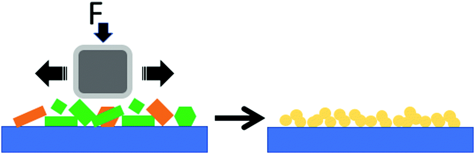
Here, we investigated the application of rubbing in thin-films, a simple and versatile technique which provides an important technological opportunity to control polymorphism. Fig. 1 shows a scheme of rubbing.
 | ||
| Fig. 1 Scheme of application of rubbing. | ||
Qualitatively, rubbing can be performed in any laboratory by swiping a piece of paper over the material deposited on a rigid support or by scratching it using a spatula. It can be performed in a controlled manner and over a large scale by using appropriate instrumentation from macroscopic size to the sub-micro and nanometric scale when performed using the tip of an atomic force microscope.17–19 Despite its versatility, to the best of our knowledge, rubbing has never been used to directly change the polymorph structure in thin films.
Here we present an unusual application of rubbing to reorganize the morphology and the crystal structure of a thin film, which is usually characterized by the co-presence of polymorphic phases. We applied rubbing to a thiophene-basedorganic semiconductor to induce a reversible fluorescence switching in films by mechanical amorphisation followed by thermal recrystallization.
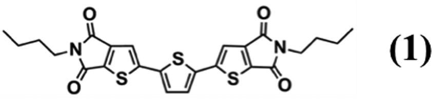
As a model material we used 2,2′-(2,2′-thiophene-5,5′-diyl)bis((5-butyl-5H-thieno[2,3-c]pyrrole-4,6)-dione) (hereafter abbreviated 1, see the chemical structure in Fig. 2) whose synthesis is reported elsewhere.20 Compound 1 is a multifunctional organic semiconductor used in optoelectronics20 and in time–temperature integrator devices5,21,22 capable of forming two polymorphs, discernible by the fluorescence colour: form α, that exhibits yellow/orange fluorescence and form β, that displays a green/yellow fluorescence.‡22,23
 | ||
| Fig. 2 Chemical structure of 2,2′-(2,2′-thiophene-5,5′-diyl)bis((5-butyl-5H-thieno[2,3-c]pyrrole-4,6)-dione) hereafter abbreviated as compound 1. | ||
The α and β polymorphs of 1 have different mechanical properties.23 The β polymorph is prone to irreversible plastic deformation; in particular the application of a mechanical force on (100) plane causes slippage of adjacent π-stacked layers, giving rise to an irreversible plastic deformation of the crystals. When the mechanical force is applied to different faces the crystals become very fragile. The α polymorph does not show any preferential slippage plane and exhibits a stronger interaction between the crystal plane. Within a small deformation the α polymorph can be elastically deformed when an external force is applied perpendicular to the (001) face. However, upon the application of a strong mechanical perturbation also the α crystals are very fragile.
In thin films, the polymorph composition can be controlled by processing such as wet lithographic assisted methods22 and by deposition in confinement both with24 and without25 physical barriers. Importantly, the α polymorph thermally converts to the β polymorph by heating at 205 °C in the bulk material25 while in thin films it starts to convert above 90 °C.
Results and discussion
Deposits of 1 were prepared by drop-casting a 1 g l−1 solution of 1 in toluene on Si/SiO2 (thermal) substrates (1 × 1 cm2).26 We deposited 10 μl for thin deposits and 200 μl for thick deposits. Samples were prepared in air and characterized by fluorescence microscopy (FM), X-ray diffraction (XRD), atomic force microscopy (AFM) and time-resolved photoluminescence (PL) in confocal fluorescence microscopy (CFM).Compound 1 has a strong tendency to form large crystals on the surface (Fig. 3a) whose sizes range from the micrometric to the millimetre scale.25 From FM images, we measured a coverage of 40 ± 20% for thin deposits and 60 ± 25% for thick deposits (see also the ESI†). The considerable variation in the coverage is intrinsic in drop-casting that produces inhomogeneous deposits. When prepared by drop casting the morphology differs for the centre and the border of the drop cast deposit. At the border large crystals are observed while in the central region smaller structures are located; this behaviour, common in drop casting, is due to the so called “coffee stain effect”.27 We did not observe the significant presence of the material in between the crystals by AFM or FM. The polymorph percentage, measured from FM images, ranges from 45% to 20% of the α phase and 55% to 80% of the β phase depending on the experimental conditions.
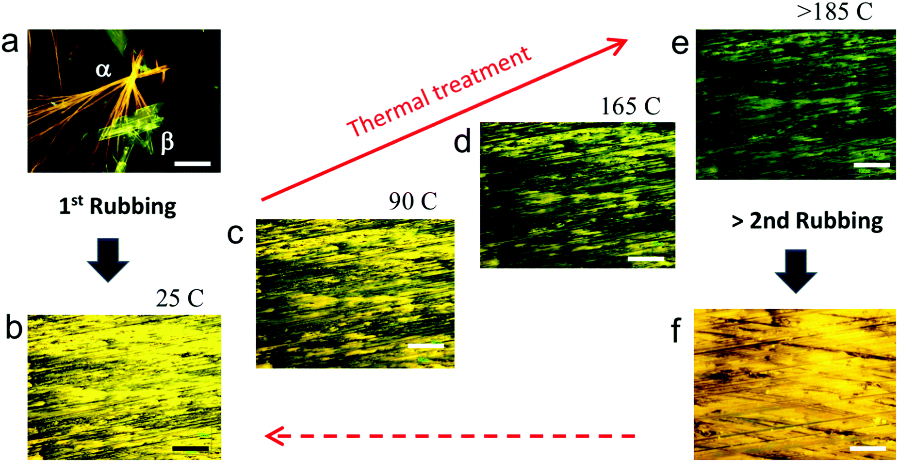 | ||
| Fig. 3 Evolution of morphology and fluorescence of 1 film after the rubbing process. Scale bars are 50 μm in all images. (a) Fluorescence image of the drop cast film from toluene solution on silicon recorded at 25 °C. (b) Fluorescence image of the film shown in “a” after the first application of rubbing. (c–e) Evolution of fluorescence images recorded during thermal treatment at (b) 25 °C (c) 90 °C, (d) 165 °C, (e) 185 °C. Above 185 °C, the fluorescence colour remains unaltered also after cooling the sample at room temperature. (f) Fluorescence image after the rubbing reapplication at 25 °C. | ||
When observed by AFM, large crystals show the typical morphology of crystals with flat surfaces and large terraces (Fig. 5a).
Rubbing was performed via paper supported on a plastic chisel and applying a vertical pressure of 100 g mm−2 and lateral motion at 50 cm s−1 on the entire sample. The process was applied at least six times for thin deposits and at least ten times for thick deposits. When applied on drop cast deposits, the process removes 30 ± 10% of the material while applied on already rubbed film removes <10% of the material. Rubbing dramatically changes the chemical–physical properties of deposits (Fig. 3 and 5). First, it turns the inhomogeneous deposits into a continuous thin film. Rubbed samples appear to be made of elongated structures oriented along the rubbing direction with a coverage of 95 ± 5% of the surface. Unlike drop casted films, rubbed films appear homogeneous in the entire sample area (Fig. 3b and 4b). No evidence of residual large crystals was observed by optical microscopy and AFM in rubbed samples. When observed by FM (Fig. 3b and f), rubbed films appear entirely yellow. Heating the rubbed films above 90 °C, the fluorescence colour starts to turn from yellow to green, the transformation is complete at ca. 190 °C. The rate of colour turning is proportional to temperature and time; nevertheless, the entire film turns to a green fluorescence colour at the end of the process (Fig. 3c–e). Notably, the process is fully reversible: applying rubbing on the thermally treated films, they turn back to the yellow fluorescent phase (Fig. 3f). We repeated the process “rubbing → thermal treatment → rubbing” for five cycles without observing any difference in the optical and structural properties of the films. Above 5 cycles the film starts to become inhomogeneous, showing large zones free of materials.
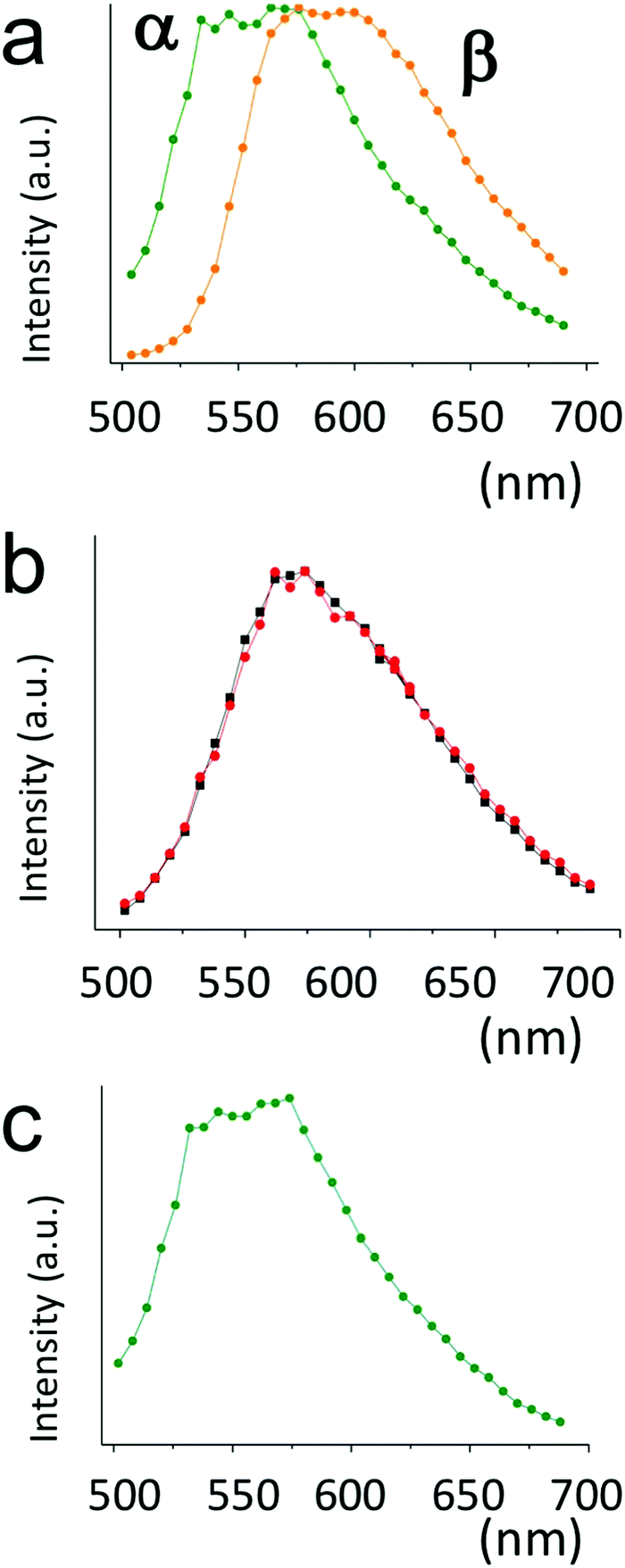 | ||
| Fig. 4 Confocal florescence spectra of (a) drop cast film from toluene solution on silicon recorded at 25 °C corresponding to the image in Fig. 3a. (b) The same film shown in “a” after the first application of rubbing, corresponding to the image in Fig. 3b (red curve) and in Fig. 3f (back curve). (c) Confocal fluorescence spectra of recorded at room temperature after treatment at 185 °C, corresponding to Fig. 3e. | ||
The nature of the turning of the fluorescence colour was investigated by PL-CFM spectroscopy and XRD.
Time-resolved photoluminescence by confocal fluorescence microscopy
In line with the previous study on the photophysical properties of the crystals obtained by drop casting of 1 from toluene solution, the α phase crystals exhibit a broad emission spectrum centred at 585 nm and the β phase crystals a spectrum centred at 540 nm (Fig. 4a). Time-resolved fluorescence lifetime imaging measured in the ranges of 500–540 nm and 565–605 nm evidenced that the fluorophore 1 experiences at least two locally different environments.22Analysing the fluorescence decay at 520 nm with a bi-exponential function, the fluorophore in the β phase has a dominating lifetime of 0.4 ns and a second lifetime of 1.0 ns, representing 20% of collected photons. For the α phase crystals a lifetime of 1.0 ns strongly prevails and a longer lifetime contributes only marginally to emission.
After rubbing the samples show a unique yellow fluorescence spectrum at around 570 nm (Fig. 4b). Examining different areas in the sample, we obtained two distinct lifetimes, a shorter one of 0.5–0.6 ns and a longer one of 1.1 ns, respectively but with different weights. The latter is very similar to the dominating lifetime of the α phase, while the shorter resembles that of the green emitting β phase. Note that β phase emission is also expected to contribute at 585 nm. The spatially more detailed investigation by CFM shows that the mechanical action exerted destroys both type of crystals but the action is likely not homogenous, thus resulting in different contributions of the two lifetimes depending on the sample area examined (see the ESI† for some figures of spatula scratched samples). Overall the mechanical action seems to fully eliminate the β phase.
After the thermal treatment the sample the spectrum dramatically changes in all areas of the sample, exhibiting a unique spectrum similar to the β phase spectrum peaking in green (Fig. 4c). We further assist an evolution to a single exponential decay with a lifetime of 0.5 ns, the latter in line with the decay parameters obtained for the β polymorph.
The confocal study with much higher spatial resolution evidencing the transformation between the two polymorphs is sometimes not complete upon mechanical action both from the spectral and fluorescence decay point of view, but overall is perfectly in line with the macroscopic observations. Differently, heating favours a more complete transition to the β polymorph.
The application of rubbing after heating again switches the PL colour to the pre-thermal treatment state (cf.Fig. 3e, f and 4b, c).
Atomic force microscopy
AFM (Fig. 5b) confirms the dramatic morphological changes induced by rubbing: rubbed films appear to be made of elongated structures and grooves oriented along the rubbing direction. Importantly, rubbed films show a significant nano- and micro-scale morphology change after thermal treatment (Fig. 5c) which is not detectable via large scale optical microscopy (indicatively when observing areas larger than 100 × 100 μm2), but is easily detected via AFM. Interestingly, the resulting morphology still exhibits crystalline features such as terraces and grain boundaries (Fig. 5c, arrow).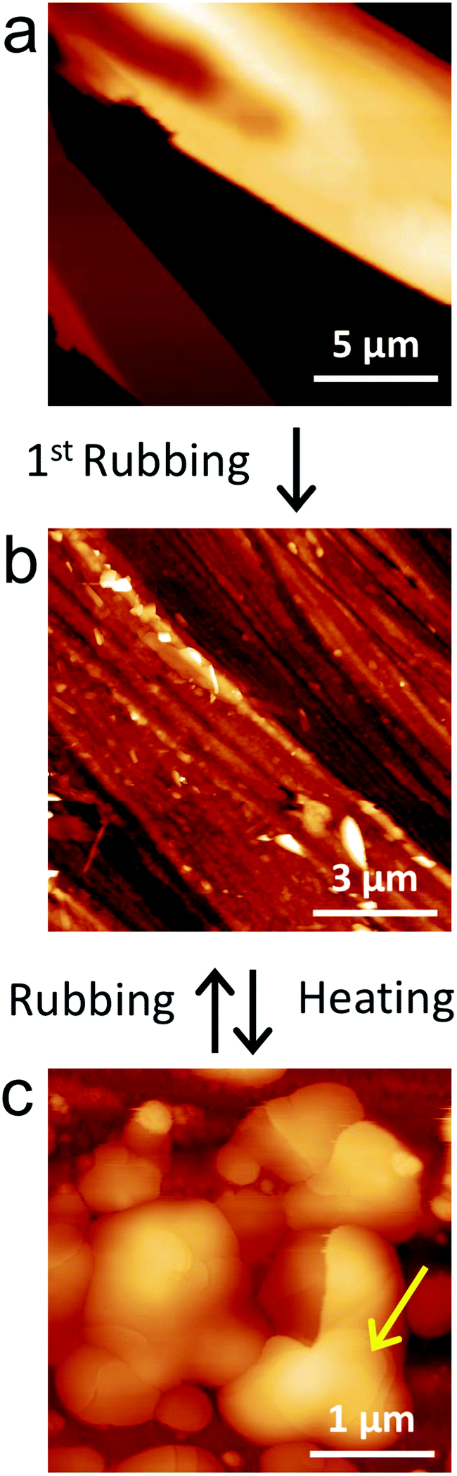 | ||
| Fig. 5 Atomic force microscopy image of (a) drop cast film (Z scale 0–300 nm). (b) The same film after rubbing (Z scale 0–200 nm) and (c) after thermal treatment (Z scale 0–300 nm). The arrow indicates some terraces. | ||
X-Ray diffraction
The effect of the rubbing process and thermal treatment on the crystal structure was assessed by means of XRD. Fig. 6 shows the XRD patterns of the film after drop casting, after rubbing, and after 30 minutes of thermal annealing. Samples prepared by drop casting exhibit the typical XRD pattern, with the Bragg peaks coming from two different α and β crystal phases, indicating the coexistence of both α and β polymorphs.23,25 Both polymorphs are oriented with the long axis almost perpendicular to the substrate surface, i.e. (001) and (100) planes for α and β respectively. After rubbing, no peaks coming from the β polymorph are observed in the spectra. Heating the sample under a nitrogen atmosphere at 190 °C, XRD measurements revealed a strong increase of Bragg peaks coming from the β crystal phase. These results suggest that during the rubbing almost all crystals of the β polymorph become amorphous, while some traces of the the α polymorph remain on the substrate.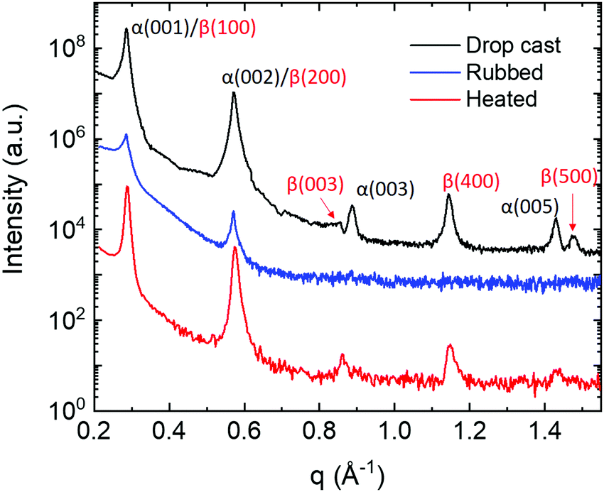 | ||
| Fig. 6 XRD patterns of 1 sample before (black line) and after (blue line) rubbering, and after thermal annealing (red line). | ||
Nano rubbing
The particular mechanical properties of 1 were exploited via SPM lithography (SPL) by applying a controlled mechanical perturbation to a crystal in the form of repeated contact-mode scanning at a known applied force. Above a threshold force of about 200 nN (an indicative value which depends on the radius and the status of the AFM tip) the mechanical perturbation produces surface scratching, resulting in the formation of grooves in the crystal terraces. Fig. 7 shows the effect of such scratching on an α crystallite.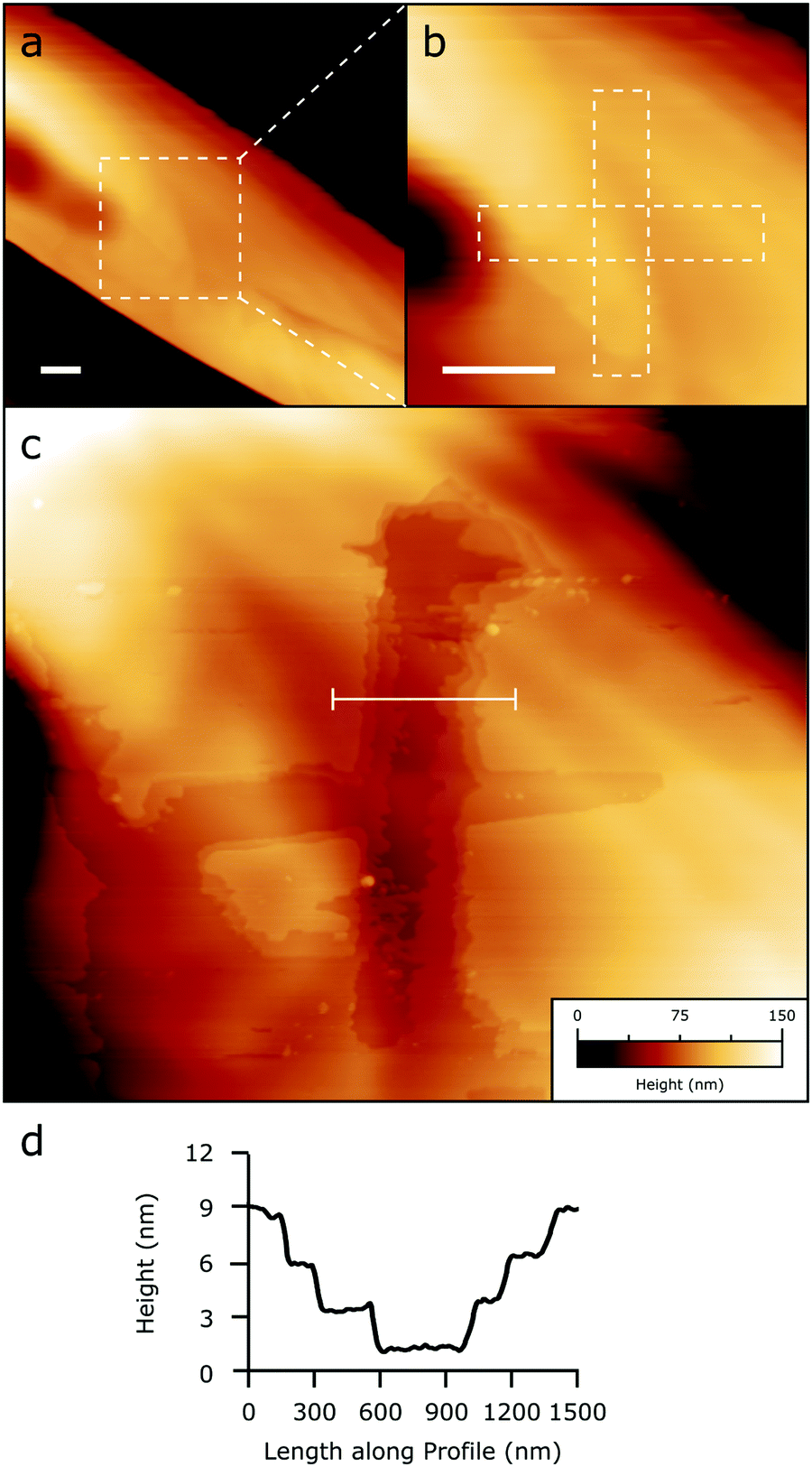 | ||
| Fig. 7 Demonstration of nanoscale rubbing via SPL. (a) Representative isolated crystal of 1 (scale bar: 2 μm). Dashed lines delimit the zone scanned in panel b. (b) Application of rubbing at controlled force via contact mode AFM (scale bar 2 μm). Dashed lines delimit two 5 × 1 μm areas subjected to repeated scanning in contact mode (see main text). (c) Result of SPL rubbing observed via PeakForce imaging at low applied force (see main text). (d) Height measured along the dashed line in panel c, evidencing crystalline terraces around 2.7 nm high. | ||
Remarkably, the scratching produces a groove without apparently altering the crystallite's main structure; moreover, it removes material layer by layer inducing highly spatially controlled delamination (Fig. 7). At the end of the process, crystal terraces are still well visible inside the scratched zone. This characteristic is very rare in SPL performed by scratching, and it enables the modeling of the crystal while also preserving its crystal integrity at the nano- and mesoscales.
Discussion
All methods employed for the characterization suggest that rubbing induces an amorphisation of crystal 1. The evidence that the temperature has an opposite effect with respect rubbing, i.e. heating causes film recrystallization toward the β polymorph, clearly indicate that the amorphisation is merely mechanical.The evidence that the β polymorph, prevalent in drop cast films, entirely disappears by rubbing is probably due to its plastic deformability related to its particular crystal structure, i.e. to the weak interaction between adjacent π-stacked layers. In the case of form α the surface is rough, while in form β the (100) is smooth and it corresponds to the slippery plane (Fig. 8).
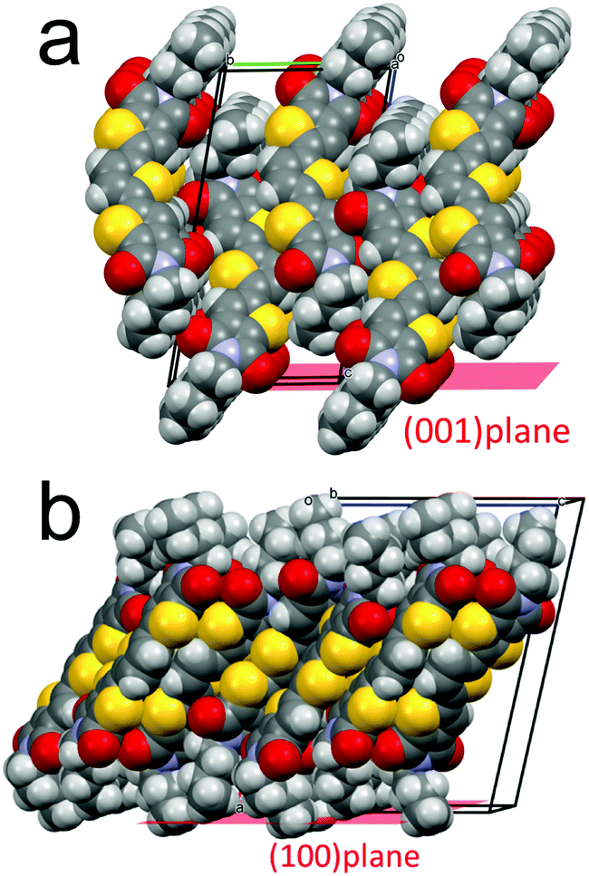 | ||
| Fig. 8 Packing of the molecule in (a) the α phase and (b) the β phase. | ||
When a force is applied the crystal plastically deforms by slippage of adjacent layers with the development of defects and delamination until its complete fragmentation leads to the amorphisation. This characteristic also explains the particular behaviour observed inducing mechanical perturbation by AFM on the terrace of a crystal.
It is interesting that the amorphisation of the metastable β phase is not followed by recrystallization into the stable phase α, although the residual presence of crystals of the stable α polymorph should act as seeds. The amorphisation of phase β is confirmed by the XRD and the CFM measurements. It is worth noting that the recrystallization which starts at 90 °C in thin films, leads to the formation of form β, and not α, even if the latter form should be stable up to 205 °C.23 Eventually, XRD measurements show that the rubbing–heating process induces a preferential orientation with the plane (100) for the β phase parallel to the substrate.
The amorphisation is due to the delamination of the crystals caused by rubbing, which greatly increases the surface area of the film. This reorganisation favours the β phase which becomes more stable with respect to α also at 90 °C, probably because of a lower surface energy of the β phase, as already observed in other systems, when the surface energy of the crystal became comparable to the contribution of the bull energy, a different polymorph becomes more stable.28 This observation can also explain the different behaviour observed in the thin film and bulk structure.
Conclusions
In conclusion we presented an unusual application of rubbing to reorganize the morphology and the structure of a model material characterized by polymorphism. The procedure transforms an inhomogeneous thin deposit in a continuous thin film, changing its crystalline structure, by mechanical amorphisation and thermal annealing. Although amorphisation is usually an unwanted process for almost every technological application, it can offer other opportunities for less conventional applications such as in time–temperature integrators and smart-paper.29 In particular the reversibility of the fluorescence colour paves the way for a new generation of regenerable time-temperature integrators devices, moreover. Here we used thiophene-basedoligomer 1 as representative material but in principle this process could be easily extended to other molecular materials and polymers.Experimental
Thin deposits
Films of 1 were prepared by drop-casting a solution 1 g l−1 in toluene of 1 on Si/SiO2 (thermal) substrates 10 × 10 mm2. We deposited 10 μl for thin films and 200 μl for thick films.Thermal treatment
Thermal treatments were performed in air under an optical microscope in FM configuration using a heating stage Linkham TMHS600 connected to a TP94 controller, with a control of 0.1 °C. The setup is described in detail in ref. 30. Sample heating was performed at the rate of 5 °C min−1. The FM images were acquired, stopping the heating for a few seconds at the indicated temperature.X-Ray diffraction
XRD was performed in specular geometry using a SmartLab-Rigaku diffractometer equipped with a rotating anode (Cu λα = 1.5405 Å), followed by a parabolic mirror to collimate the incident beam, and a series of variable slits (placed before and after the sample position) to reach an acceptance of 0.01°. Index of the peaks were attributed considering the structure published in the ref. 23.Fluorescence microscopy
Fluorescence images were recorded with a Nikon i-80 microscope equipped with epi-fluorescence (FM) using FM filter Nikon Ex 420, DM 435, BA 475 and Ex 535, DM 570, BA 590. The FM images were recorded using a commercial CCD camera (Nikon CCD DS-2 Mv). The illumination was performed by a 100 W Hg lamp at fixed power.Measurement of polymorph percentage and coverage
Coverage and polymorph percentages were measured from FM images using home-made software capable of extracting the number of pixels of a defined colour from an image. Black pixels are associated with a clean surface; yellow-orange pixels are associated with the α phase and green pixel with the β phase. The percentage of a specific polymorph is calculated as the number of pixels associated with a defined colour and the total number of pixels of the image. The coverages are calculated as the ratio of the sum of all coloured pixels (i.e. “α” and “β” pixels) and the total number of pixels of the analysed image.Confocal microscopy
Confocal fluorescence imaging was performed on an inverted Nikon Ti-E microscope (Nikon Co., Shinjuku, Japan) using an argon-ion CW laser as well as 405 nm pulsed/CW diode lasers (PicoQuant GmbH, Berlin, Germany). Images were collected using a Nikon Plan Apo VC 20× air objective with NA 0.8. Filters were set to register the fluorescence intensity in the 510–540 nm, 555–615 nm and 665–735 nm ranges. A Nikon A1 spectral module with a precisely corrected 32-PMT array detector was used for spectral imaging. The wavelength resolution was set to 6 nm per PMT array. Spectral images were obtained by exciting the sample at 488 nm in CW mode.Atomic force microscopy
AFM imaging was performed on a Multimode 8 microscope equipped with a Nanoscope V controller and type J piezoelectric scanner (Bruker, USA). Samples were scanned at 0.5 Hz per line in PeakForce mode using ScanAsyst-Air probes (Bruker, USA) in air, imposing an applied force of 2.5 nN. Nanoscratching tests were performed in contact mode with an imposed force of 200 nN. Background interpolation and quantitative surface characterization were performed with Gwyddion 2.37 (http://gwyddion.net/).Conflicts of interest
There are no conflicts to declare.Acknowledgements
This work is dedicated to Jaume Veciana and Concepció Rovira, two extraordinary persons and outstanding scientists. We are grateful for the financial support provided by the Italian Minister of instruction, university and research, National project PRIN “Next generation of molecular and supramolecular machines: towards functional nanostructured devices, interfaces, surfaces and materials (NEMO)” Prot. 20173L7W8K and National project PRIN “Novel Multilayered and Micro-Machined Electrode. Nano-Architectures for Electrocatalytic Applications”. Prot. 2017YH9MRK.Notes and references
- D. Gentili, M. Gazzano, M. Melucci, D. Jones and M. Cavallini, Chem. Soc. Rev., 2019, 48, 2502–2517 RSC.
- M. Cavallini, J. Mater. Chem., 2009, 19, 6085–6092 RSC.
- S. Hashmi, Reference Module in Materials Science and Materials Engineering, Elsevier, 2016 DOI:10.1016/B978-0-12-803581-8.04101-1.
- T. Mallah and M. Cavallini, C. R. Chim, 2018, 21, 1270–1286 CrossRef CAS.
- M. Cavallini, A. Calo, P. Stoliar, J. C. Kengne, S. Martins, F. C. Matacotta, F. Quist, G. Gbabode, N. Dumont, Y. H. Geerts and F. Biscarini, Adv. Mater., 2009, 21, 4688–4691 CrossRef CAS.
- E. Bystrenova, M. Facchini, M. Cavallini, M. G. Cacace and F. Biscarini, Angew. Chem., Int. Ed., 2006, 45, 4779–4782 CrossRef CAS PubMed.
- E. Gomar-Nadal, J. Puigmarti-Luis and D. B. Amabilino, Chem. Soc. Rev., 2008, 37, 490–504 RSC.
- M. Melucci, M. Zambianchi, L. Favaretto, V. Palermo, E. Treossi, M. Montalti, S. Bonacchi and M. Cavallini, Chem. Commun., 2011, 47, 1689–1691 RSC.
- P. Balaz, M. Achimovicova, M. Balaz, P. Billik, Z. Cherkezova-Zheleva, J. M. Criado, F. Delogu, E. Dutkova, E. Gaffet, F. J. Gotor, R. Kumar, I. Mitov, T. Rojac, M. Senna, A. Streletskii and K. Wieczorek-Ciurowa, Chem. Soc. Rev., 2013, 42, 7571–7637 RSC.
- S. L. James, C. J. Adams, C. Bolm, D. Braga, P. Collier, T. Friscic, F. Grepioni, K. D. M. Harris, G. Hyett, W. Jones, A. Krebs, J. Mack, L. Maini, A. G. Orpen, I. P. Parkin, W. C. Shearouse, J. W. Steed and D. C. Waddell, Chem. Soc. Rev., 2012, 41, 413–447 RSC.
- X. Du, F. Xu, M.-S. Yuan, P. Xue, L. Zhao, D.-E. Wang, W. Wang, Q. Tu, S.-W. Chen and J. Wang, J. Mater. Chem. C, 2016, 4, 8724–8730 RSC.
- G. Q. Zhang, J. W. Lu, M. Sabat and C. L. Fraser, J. Am. Chem. Soc., 2010, 132, 2160–2162 CrossRef CAS PubMed.
- J. W. Chung, Y. You, H. S. Huh, B. K. An, S. J. Yoon, S. H. Kim, S. W. Lee and S. Y. Park, J. Am. Chem. Soc., 2009, 131, 8163–8172 CrossRef CAS PubMed.
- M. Cavallini, Science, 2003, 299, 662 CrossRef PubMed.
- W. S. Hu, Y. F. Lin, Y. T. Tao, Y. J. Hsu and D. H. Wei, Macromolecules, 2005, 38, 9617–9624 CrossRef CAS.
- D. E. Lee, J. Ryu, D. Hong, S. Park, D. H. Lee and T. P. Russell, ACS Nano, 2018, 12, 1642–1649 CrossRef CAS PubMed.
- G. Derue, S. Coppee, S. Gabriele, M. Surin, V. Geskin, F. Monteverde, P. Leclere, R. Lazzaroni and P. Damman, J. Am. Chem. Soc., 2005, 127, 8018–8019 CrossRef CAS PubMed.
- G. Derue, D. A. Serban, P. Leclere, S. Melinte, P. Damman and R. Lazzaroni, Org. Electron., 2008, 9, 821–828 CrossRef CAS.
- M. Melucci, L. Favaretto, A. Zanelli, M. Cavallini, A. Bongini, P. Maccagnani, P. Ostojo, G. Derue, R. Lazzaroni and G. Barbarella, Adv. Funct. Mater., 2010, 20, 445–452 CrossRef CAS.
- M. Durso, C. Bettini, A. Zanelli, M. G. Lobello, F. De Angelis, V. Biondo, D. Gentili, R. Capelli, M. Cavallini, M. Muccini and M. Melucci, Org. Electron., 2013, 14, 3089–3097 CrossRef CAS.
- M. Cavallini and M. Melucci, ACS Appl. Mater. Interfaces, 2015, 7, 16897–16906 CrossRef CAS PubMed.
- D. Gentili, M. Durso, C. Bettini, I. Manet, M. Gazzano, R. Capelli, M. Muccini, M. Melucci and M. Cavallini, Sci. Rep., 2013, 3, 2581 CrossRef PubMed.
- C. Cappuccino, L. Catalano, F. Marin, G. Dushaq, G. Raj, M. Rasras, R. Rezgui, M. Zambianchi, M. Melucci, P. Naumov and L. Maini, Cryst. Growth Des., 2020, 20, 884–891 CrossRef CAS.
- D. Gentili, F. Valle, C. Albonetti, F. Liscio and M. Cavallini, Acc. Chem. Res., 2014, 47, 2692–2699 CrossRef CAS PubMed.
- D. Gentili, I. Manet, F. Liscio, M. Barbalinardo, S. Milita, C. Bettini, L. Favaretto, M. Melucci, A. Fraleoni-Morgera and M. Cavallini, Chem. Commun., 2020, 56, 1689–1692 RSC.
- M. Cavallini, Z. Hemmatian, A. Riminucci, M. Prezioso, V. Morandi and M. Murgia, Adv. Mater., 2012, 24, 1197–1201 CrossRef CAS PubMed.
- R. D. Deegan, O. Bakajin, T. F. Dupont, G. Huber, S. R. Nagel and T. A. Witten, Nature, 1997, 389, 827–829 CrossRef CAS.
- A. M. Belenguer, A. J. Cruz-Cabeza, G. I. Lampronti and J. K. M. Sanders, CrystEngComm, 2019, 21, 2203–2211 RSC.
- W. Yang, C. Liu, S. Lu, J. Du, Q. Gao, R. Zhang, Y. Liu and C. Yang, J. Mater. Chem. C, 2018, 6, 290–298 RSC.
- A. Calo, P. Stoliar, M. Cavallini, Y. H. Geerts and F. Biscarini, Rev. Sci. Instrum., 2010, 81, 033907 CrossRef PubMed.
Footnotes |
| † Electronic supplementary information (ESI) available. See DOI: 10.1039/d1tc01036k |
| ‡ In some papers the name of α and β polymorphs are different. |
| This journal is © The Royal Society of Chemistry 2021 |