
 Open Access Article
 This Open Access Article is licensed under a Creative Commons Attribution-Non Commercial 3.0 Unported Licence
Improving electron injection and transport in polymer field-effect transistors with guanidino-functionalized aromatic n-dopants†
Severin
Schneider
a,
Jan M.
Gotthardt
a,
Lena
Steuer
b,
Simone
Leingang
b,
Hans-Jörg
Himmel
 b and
Jana
Zaumseil
*a
b and
Jana
Zaumseil
*a
aInstitute for Physical Chemistry and Centre for Advanced Materials, Universität Heidelberg, D-69120 Heidelberg, Germany. E-mail: zaumseil@uni-heidelberg.de
bInstitute for Inorganic Chemistry, Universität Heidelberg, D-69120 Heidelberg, Germany
First published on 28th May 2021
Abstract
The application of n-dopants in organic field-effect transistors (FETs) enables improvement of electron injection and transport. They can block hole injection and suppress ambipolar transport, thus creating purely n-type devices with large on/off current ratios. Here, we apply guanidino-functionalized aromatic (GFA) compounds such as 1,2,4,5-tetrakis(tetramethylguanidino)benzene (ttmgb) and 1,2,4,5-tetrakis(N,N′,-dimethyl-N,N′-ethyleneguanidino)benzene (tdmegb) as two-electron donors (n-dopants) with similar redox properties but different solubilities in bottom-contact/top-gate FETs with mostly electron-transporting but still somewhat ambipolar polymer semiconductors P(NDI2OD-T2) and DPPT-BT. The resulting n-type FETs show lower contact resistance and no hole transport while avoiding undesired onset voltage shifts and maintaining high electron mobilities, low hysteresis, and high stability under bias stress in ambient air. Various methods of integrating the GFA-dopants are explored (as injection layers on the electrodes, polymer-dopant blends and by deposition on top of the semiconducting layer) to identify the optimal process for the respective polymer-dopant combination.
Introduction
Many applications of organic field-effect transistors (OFETs) have been demonstrated over the last decade such as flexible displays, sensors and various electronic circuits.1–3 Nevertheless, several challenges remain. Among them is the fabrication of stable, high-mobility and purely n-type OFETs with low contact resistance. Despite substantial progress, n-type OFETs still show lower performance than p-type OFETs.4 Both types of transistors are required for efficient and low-power complementary circuits, ideally with balanced mobilities and high on/off current ratios. At the same time, ambipolarity should be avoided or suppressed to reduce power dissipation.5 Achieving efficient electron injection and thus low contact resistance in n-type OFETs is a challenge especially when using air-stable contacts with high work functions (e.g., gold). Large contact resistance not only leads to undesired voltage drops at the contacts6,7 but also limits the maximum frequency at which the transistors can switch and circuits can operate.8,9The device performance of p- and n-type OFETs in general can be improved substantially by the application of the corresponding molecular dopants.10,11 Dopants can enhance charge carrier injection (contact doping),12–16 reduce the number of trap states in the channel,12,15,17 control the threshold voltage,12,14–16,18 and suppress injection of opposite charge carriers12,19,20 (i.e., ambipolar characteristics). Contact doping is the most common approach for OFETs to reduce the injection barriers for charges and hence contact resistance.13,16,21 This is achieved by lowering the Schottky barrier height and making the depletion layer thinner, which allows charge carriers to tunnel through. Channel or bulk doping, which are usually implemented by blending semiconductor and dopant, enable control of the threshold voltage, neutralize trap states and improve device stability.18,22,23 Furthermore, diffusion of dopant molecules into or through the semiconducting layer is an alternative to blending that can help to maintain the morphology of the semiconductor.12,24,25 Importantly, doping in OFETs is generally not intended to permanently increase the number of mobile charge carriers10,11 and hence the conductivity of the semiconducting layer as is the case for thermoelectric devices.26 Such degenerate doping would lead to large off-currents and prevent or reduce the modulation of carrier concentration in the channel and thus drain current by the applied gate voltage. Consequently, the concentration, redox potentials and location of the applied dopants must be optimized.
While significant progress has been made for p-type transistors, n-doping is much more challenging. Since n-dopants should be strongly reducing, they are also highly sensitive to air and moisture. These properties pose a challenge for processing and stable device operation.11,27 Typical n-dopants for OFETs include inorganic salts (CsF),12 tetrabutylammonium salts,28 small molecules such as benzyl viologen29 or dihydrodimethylbenzimidazole23 and metallocene30 derivatives, that can also be dimerized31 for enhanced yet still rather limited environmental stability. Some of these dopants have been employed successfully in polymer FETs.28–30 However, n-dopants that are easy to process and allow for precise control of all relevant parameters while also avoiding unstable device operation, diminished on/off current ratios or insufficient control over power dissipation, remain to be found.
We recently introduced the guanidino-functionalized aromatic (GFA) compound 1,2,4,5-tetrakis(tetramethylguanidino)benzene (ttmgb) as a contact dopant with hole-blocking properties for purely n-type field-effect transistors based on semiconducting single-walled carbon nanotube networks.19,32,33 The electron donating ttmgb was found to reduce the work function of various metals by about 1 eV as determined by previous Kelvin probe measurements,33 thus lowering the Schottky barrier for electron injection drastically and decreasing contact resistance. A secondary effect was the suppression of hole injection by the oxidized species ttmgb2+ created at the metal surface.19 Moreover, residual water often adsorbed on polar surfaces (e.g., glass), which typically creates electron traps for carbon nanotubes34 and organic semiconductors,35,36 was removed by protonation of ttmgb due to its high alkalinity.19,37
Here, we apply ttmgb and another GFA, i.e., 1,2,4,5-tetrakis(N,N′-dimethyl-N,N′-ethyleneguanidino)benzene (tdmegb), with similar redox potential but different solubility in organic solvents to FETs based on the two widely used polymer semiconductors, P(NDI2OD-T2) (poly[N,N′-bis(2-octyldodecyl)-naphthalene-1,4,5,8-bis(dicarboximide)-2,6-diyl]-alt-5,5′-(2,2′-bithiophene))38–40 and DPPT-BT (poly[(2,5-bis(2-octyldodecyl)-(5(benzo[2,1,3]thiadiazole-4,7-diyl)-2,5-diyl)-thiophen-2,5-diyl)6-(thiophen-2,5-yl)pyrrolo[3,4-c]pyrrole-1,4(2H,5H)dione)]).41,42 We explore the impact of the GFA dopants on device performance and in particular on contact resistance in bottom-contact/top-gate FETs depending on the mode of dopant application. For both polymers we achieve significant improvement of electron injection together with effective suppression of hole transport while maintaining low hysteresis, high electron mobilities and stable operation under bias stress in air.
Results and discussion
In this study, we used bottom-contact/top-gate field-effect transistors (FETs) with spin-coated thin films of electron-transporting polymers (P(NDI2OD-T2) and DPPT-BT) and a hybrid dielectric of poly(methyl methacrylate) (PMMA)/HfOx to minimize the number of trap sites while also enabling low-voltage and air-stable operation.43 We investigated three different methods to integrate the two GFA dopants (bottom injection layer, bulk blend and top layer) as shown in Fig. 1a. Based on our previous work on nanotube networks,19,32,33 either an injection layer was deposited onto the substrate and electrodes before spin-coating the polymer, a blend of dopant with the semiconducting polymer was applied, or a top layer of dopant was deposited onto the semiconductor. Physical vapor deposition of both GFA compounds (ttmgb and tdmegb, see molecular structures in Fig. 1b) in vacuum as well as spin-coating of ttmgb solution in toluene were employed. | ||
| Fig. 1 Device architectures and molecular structures, (a) bottom-contact/top-gate field-effect transistors, from top: dopant (red) deposited as injection layer (prior to semiconducting polymer, blue); dopant-polymer mix deposited as a blend; dopant added after deposition of the polymer as a top layer. (b) Oxidation reaction of ttmgb as a reversible two-electron donor to ttmgb2+; structural difference between ttmgb (tetramethyl, red) and tdmegb (dimethylethylene, blue). (c) Molecular structures of the semiconducting polymers P(NDI2OD-T2) and DPPT-BT. | ||
Both GFA dopants are highly alkaline two-electron donors that can passivate trap states caused by traces of water. They exhibit similar redox potentials (−0.76 (ttmgb) and −0.79 V (tdmegb) vs. Fc/Fc+),44 but show drastically different solubilities. Due to its larger side chain rigidity, tdmegb is only soluble in polar solvents (e.g., N-methyl-2-pyrrolidone) and barely soluble in toluene and chlorobenzene, which were the solvents used for the semiconducting polymers P(NDI2OD-T2) and DPPT-BT (see Fig. 1c for molecular structures), respectively. While P(NDI2OD-T2) is well-known for electron transport with high carrier mobilities,40 DPPT-BT exhibits more ambipolar characteristics although with higher electron than hole mobilities.41,42 In both cases, the goal was to improve electron injection (i.e., lower the contact resistance to avoid voltage losses), reduce hole injection and transport to maximize on/off current ratios, and thus minimize power dissipation in complementary circuits.19 These performance improvements were to be achieved without introducing hysteresis, threshold voltage shifts or disrupting the polymer morphology and hence reducing the electron mobility.
The previously established method of using ttmgb for nanotube network FETs, i.e., to use ttmgb as a contact dopant,19,32,33 served as a starting point. Fig. 2 shows the effects of depositing a thin layer of ttmgb by spin-coating and of tdmegb by physical vapor deposition before spin-coating P(NDI2OD-T2) from toluene on the final device characteristics. As tdmegb is barely soluble in toluene, the deposited layer should remain unaffected by the polymer deposition while ttmgb is expected to be partially dissolved and redistributed during the spin-coating process. The morphology of the P(NDI2OD-T2) films after deposition showed the typical ribbon-like structures, which remained largely unchanged by the presence of the dopants (see atomic force micrographs, ESI,† Fig. S1).
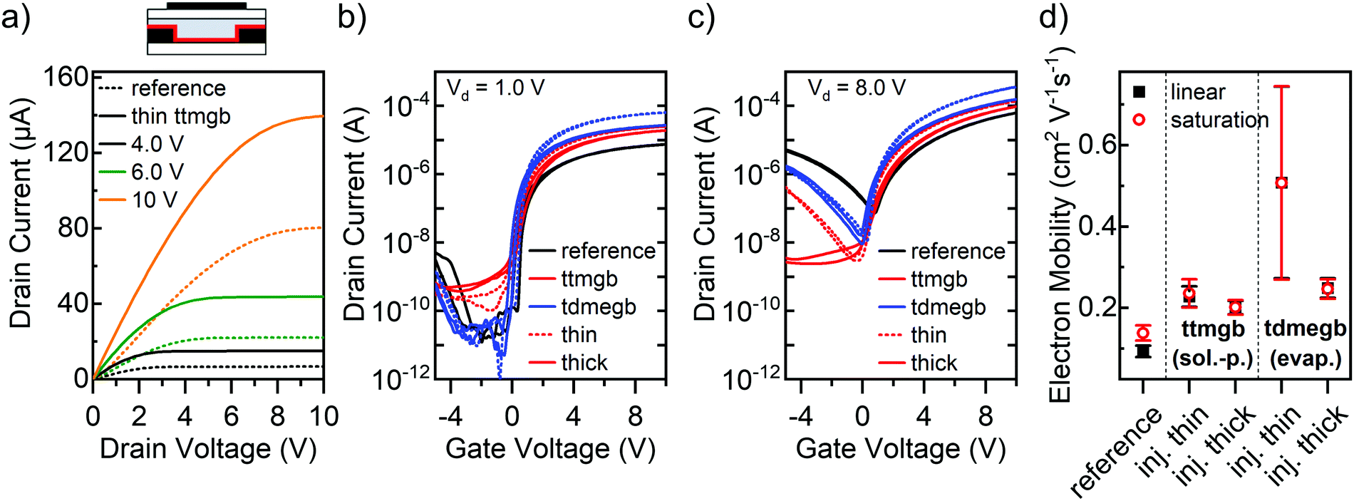 | ||
| Fig. 2 P(NDI2OD-T2) FETs (L = 40 μm, W = 5 mm) with GFA-dopant injection layers. (a) Simplified device layout and output characteristics of FET with thin ttmgb injection layer (solid lines) and untreated reference sample (dotted lines) at different gate voltages. Transfer characteristics in the linear (b) and saturation regime (c) for untreated reference sample and two dopant layer thicknesses each for solution-processed ttmgb and evaporated tdmegb. (d) Corresponding electron mobility in linear (black squares) and saturation regime (red circles). Error bars represent standard deviation based on at least 8 measured FETs. | ||
The output characteristics of the FET with a thin ttmgb injection layer displayed in Fig. 2a indicate a drastic improvement of electron injection compared to the untreated reference sample. The increase of the drain currents at low drain voltages (Vd) becomes more linear while current saturation at high Vd is maintained. Similar trends were observed for all devices (output curves are shown in Fig S2, ESI†). Transfer characteristics (red lines) in both the linear (Fig. 2b) and saturation regime (Fig. 2c) corroborate higher electron on-currents. Furthermore, a strong suppression of hole injection (from the drain electrode) and transport even at higher drain voltages is achieved. This effect increases with film thickness of ttmgb (i.e., concentration in spin-coated solution) until no hole current is observed at negative gate voltages (Fig. 2c). The apparent electron mobilities, which are within the typical range of spin-coated, commercially available P(NDI2OD-T2),39,45 also increase with doping (from 0.18 to 0.32 cm2 V−1 s−1, see Fig. 2d). Importantly, the onset voltages remain around 0 V and the hysteresis remains very low.
FETs with physical vapor-deposited thin and thick injection layers of tdmegb show a very similar effect in the linear and saturation regime transfer characteristics (Fig. 2c and d) with even higher electron mobilities although the suppression of hole injection at high drain voltages is not as good as for ttmgb. Note that the drain currents and electron mobilities for P(NDI2OD-T2) FETs with thin tdmegb injection layers are higher but also show a large spread, which is due to non-uniformity of the surface coverage of the electrodes. Several strategies (surface treatments etc.) were tested to improve the uniformity but remained unsuccessful.
Overall, electron injection from gold into P(NDI2OD-T2) improved significantly with both dopants at very moderate coverage of the gold source/drain electrodes while efficient hole current suppression could only be achieved at higher surface coverage. Clearly, contact doping and the reduction of the work function can be expected to be the main effects here as previously discussed for gold electrodes in nanotube network transistors.19,33 As charge transport occurs at the top of the polymer layer at the interface to the dielectric, it should not be affected much by the presence of the dopant. This notion is supported by the absence of any noticeable shifts in the onset voltages or significant increase in the off-current level, which would be expected for direct n-doping of the semiconductor. The actual changes in contact resistance (measured in a four-point probe geometry) and contact resistance-corrected mobility values will be presented and discussed below.
Another strategy for doping is to mix the dopants directly with the semiconducting polymer matrix during processing and thus neutralize traps in the bulk.22,46 This blending method can provide a higher film uniformity if no phase separation takes place. The ribbon-like morphology of P(NDI2OD-T2) is usually not disturbed by the addition of small amounts of other compounds and thus lends itself to direct molecular doping.47 We combined the n-dopant ttmgb with P(NDI2OD-T2) in toluene solution (for details, see Experimental section) before spin-coating and investigated the effect of the ttmgb concentration on device performance. As shown in Fig. 3a, a very low amount of dopant (0.1 wt%) already leads to significantly improved electron injection (for full output characteristics, see ESI,† Fig. S3). The on-currents increase up to a ttmgb concentration of 0.5 wt% (see Fig. 3b, linear regime, (Vd = 1.0 V) and drop again at higher concentrations (1 wt% and 2 wt% ttmgb). However, they remain above the values of the untreated references samples. While the on-currents in the saturation regime (Vd = 8.0 V, Fig. 3c) exhibit the same trend as in the linear regime, the decrease in hole current injected from the drain at negative gate voltages is most pronounced at higher ttmgb concentrations.
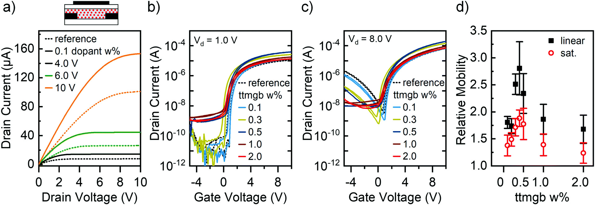 | ||
| Fig. 3 FETs (L = 40 μm, W = 5 mm) with P(NDI2OD-T2)-ttmgb blends. (a) Simplified device schematic and output characteristics of FET with blend of 0.1 wt% ttmgb (solid line) and untreated reference sample (dotted line). Transfer characteristics in the linear (b) and saturation regime (c) for untreated reference sample and blends at ttmgb concentrations in the range of 0.1–2.0 wt%. (d) Relative electron mobility of polymer blends compared to reference sample in the linear (black squares) and saturation regime (red circles) as a function of ttmgb concentration. Error bars represent mean error based on at least 8 measured FETs. | ||
Interestingly, even at moderate ttmgb concentrations of 0.5 wt% an increase in off-current that is not modulated by the gate voltage is observable, which indicates some undesired degenerate n-doping of the P(NDI2OD-T2). Given that the ionization potential of ttmgb varies depending on dielectric environment from 3.7 to 4.2 eV,48 a redox reaction with P(NDI2OD-T2) (lowest unoccupied molecular orbital (LUMO) at −4.0 eV)40 may seem possible. This notion is in agreement with a small onset voltage shift of −0.7 V for the 2.0 wt% ttmgb sample compared to the untreated reference and a lower subthreshold slope upon higher dopant loading as previously observed.14 In contrast to the injection layers discussed above, it can be assumed that for blends the dopant is also present at the semiconductor-dielectric interface, thus directly affecting the charge transport layer to some degree. However, details on a possible n-doping mechanism are not available at this time.
Electron mobilities were determined for all tested ttmgb concentrations and are depicted in Fig. 3d as relative mobilities compared to the reference sample. The relative mobility peaks at a concentration of 0.4 wt% ttmgb (absolute electron mobility 0.20–0.33 cm2 V−1 s−1) whereas the enhancement for higher concentrations is less pronounced. The stronger relative increase for the linear regime compared to the saturation regime is attributed to the larger impact of the reduced contact resistance in this regime. Even though AFM images did not show any changes in morphology (ESI,† Fig. S1f and g), a likely reason for the lower performance at higher ttmgb concentrations may be a disruption of the packing of the P(NDI2OD-T2) chains. In summary, blending the GFA-dopant ttmgb with P(NDI2OD-T2) at suitably low concentrations does indeed lead to transistor performance improvements. However, the desired low off-currents are not achieved, either due to insufficient hole blocking at low ttmgb concentrations or degenerate n-doping at higher concentrations.
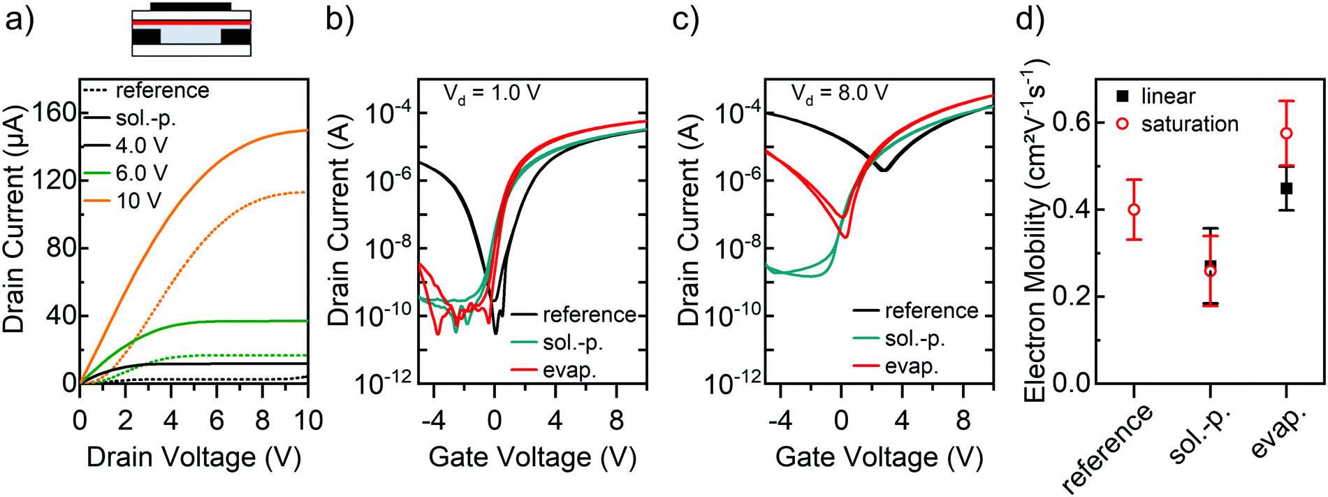
The third option is the deposition of a molecular dopant (e.g., by evaporation) on top of the semiconducting layer followed by diffusion into it. For a bottom contact/top gate transistor the dopant would be mostly located at the interface between semiconductor and dielectric where charges are accumulated (see Fig. 1a) and away from the injecting electrodes. A strong effect on transport but less on charge injection is expected. The dopant ttmgb can be deposited on top of a 30 nm thick semiconducting layer of P(NDI2OD-T2) either by thermal evaporation in vacuum or by spin-coating from solution. However, essentially all ttmgb solvents will lead to intermixing and partial dissolution of the polymer layer resulting in much thinner films.
As is evident from the output characteristics in Fig. 4a, a vapor-deposited ttmgb top layer leads to electron injection improvements very similar to the previous doping methods (for full output characteristics, see ESI,† Fig. S4). However, the drain currents are only significantly increased for lower drain voltages, which is corroborated by the corresponding transfer curves in the linear (Fig. 4b) and saturation regime (Fig. 4c). This unexpected behavior suggests that some dopant diffusion through the film – possibly aided by spin-coating the PMMA dielectric layer from n-butyl acetate – takes place and thus contact doping of the gold electrodes. As an undesired side-effect, the off-currents increase in the linear regime while only showing a moderate decrease of hole injection and transport at high drain voltages. The linear electron mobility also increased while the saturation mobility remained unchanged (see Fig. 4d), which is consistent with a reduced contact resistance (see below).
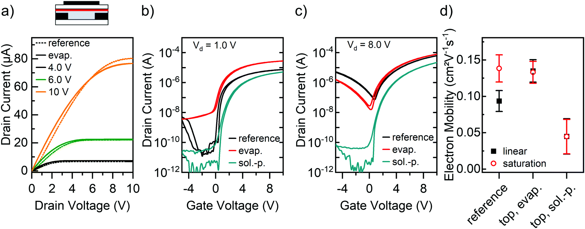 | ||
| Fig. 4 P(NDI2OD-T2) FETs (L = 40 μm, W = 5 mm) with ttmgb top layers. (a) Simplified device schematic and output characteristics of FET with ttmgb top layer (solid line) and untreated reference sample (dotted line). Transfer characteristics in the linear (b) and saturation regime (c) for untreated reference sample, vacuum-deposited (evap.) and solution-processed (sol.-p.) ttmgb top layers. (d) Corresponding electron mobility in linear (black squares) and saturation regime (red circles). Error bars represent standard deviation based on at least 10 measured FETs. | ||
Spin-coating the ttmgb on top of P(NDI2OD-T2) resulted in a quite different behavior. Even after extensive optimization of the processing conditions, the final FETs exhibited slightly lower electron currents than the corresponding reference samples (see Fig. 4b and c). Moreover, they showed a shallower subthreshold slope indicating an overall increased trap density, which may be attributed to the significantly thinner polymer film.49 AFM images indeed revealed significant changes in the morphology of the P(NDI2OD-T2) (see ESI,† Fig. S1c), such as larger roughness and decreased layer thickness (only 7 nm) compared to the untreated reference films (30 nm). The absence of any shift in onset voltage renders doping of the semiconductor unlikely. The toluene partially dissolves the P(NDI2OD-T2) during the spin-coating step and this film degradation reduces the electron mobility (see Fig. 4d).
However, full suppression of hole injection and transport at low and high drain voltages is also achieved. Overall, ttmgb deposition on top of the semiconducting polymer either by thermal evaporation or spin-coating is the least suitable method for the goal of improved electron injection and hole blocking.
To investigate the impact of GFA dopants on electron injection and hence contact resistance in P(NDI2OD-T2) FETs in more detail, a gated four-point probe transistor geometry (see Experimental section for details) was used to extract the gate voltage-dependent, width-normalized contact resistances and corrected electron mobilities in the linear regime according to the method established by Pesavento et al.50,51 Note that the absolute resistance values should be treated with caution as the P(NDI2OD-T2) films were not patterned, which can lead to an overestimation of contact resistance.51 However, given the precise alignment of the gate electrode with the channel area in addition to equal layouts for all samples, a general comparison of the extracted values is still possible. Width-normalized contact resistance values are shown in Fig. 5a. As expected, all contact resistances decrease with increasing gate voltage and are within the previously reported range for top-gated P(NDI2OD-T2) transistors.38 In all cases, the ttmgb injection layers (i.e., ttmgb deposited before polymer) led to a significant reduction of contact resistance (by approx. one order of magnitude) compared to the untreated reference samples.
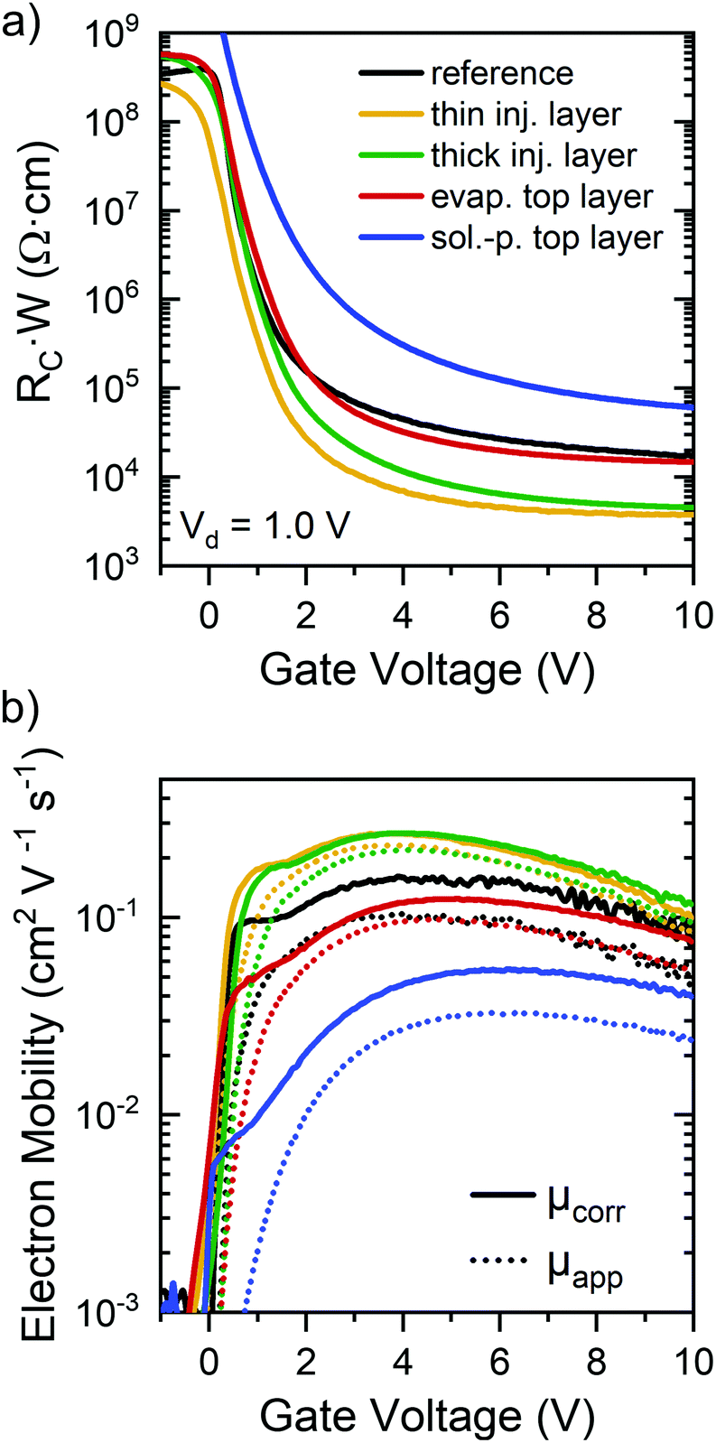 | ||
| Fig. 5 Contact resistance. (a) Gate voltage-dependent and width-normalized contact resistances of P(NDI2OD-T2) FETs (L = 40 μm, W = 1 mm) as determined by gated four-point probe measurements in the linear regime for an untreated reference sample and devices with ttmgb dopant deposited prior (thin/thick injection layer) or after (evaporated or solution-processed top layer) the polymer semiconductor. (b) Apparent (dotted lines) and contact resistance-corrected (solid lines) electron mobilities for these FETs as a function of gate voltage. | ||
Evaporated top layers of ttmgb showed a much lower impact in agreement with the discussion above. For FETs with a spin-coated top layer of ttmgb, the contact resistance actually increased, which is probably due to the very thin film thickness and hence less efficient injection from the top of the electrodes as previously observed for incomplete coverage at contact edges.49
The comparison of apparent (without correction) and contact resistance-corrected electron mobilities (Fig. 5b) in the linear regime for the different doping methods reveals only moderate changes of charge transport through the channel, especially in full accumulation (i.e., large gate voltages). Only FETs with very thin P(NDI2OD-T2) layers due to spin-coating of the ttmgb on top showed substantially lower mobilities as already discussed.
An important property of a semiconductor/dopant system is its environmental stability, referring to both the chemical stability of the involved compounds as well as the stability of the device during operation (e.g., with respect to dopant diffusion). While ttmgb can be handled in dry air for short periods of time, device processing was carried out in dry nitrogen and the hybrid dielectric of PMMA and HfOx is expected to provide sufficient self-encapsulation of the devices. To confirm the stability of FETs with ttmgb injection layers, they were subjected to continuous bias stress for 10 h in ambient atmosphere. Fig. 6a shows transfer characteristics measured immediately before and after bias stress indicating excellent stability with virtually no changes of hysteresis or on- and off-currents and only a small shift (−0.7 V) in the onset voltage. The on-current decreased by less than 10% over 10 hours of continuous bias stress (see Fig. 6b). These observed device characteristics corroborate the absence of any unwanted degradation or diffusion of the ttmgb dopant under continuous electron accumulation and bias stress. They highlight the suitability of ttmgb as a contact dopant in polymer FETs.
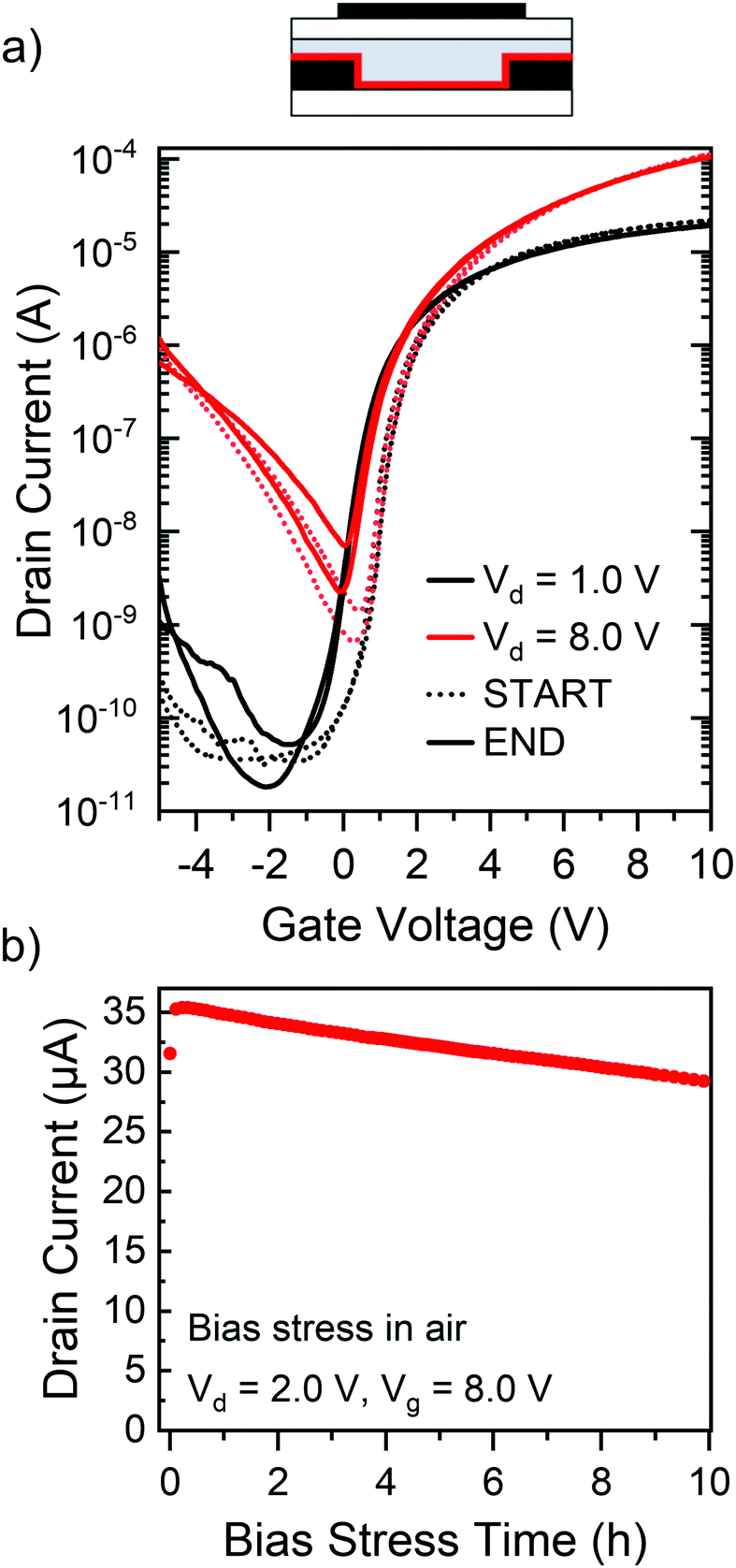 | ||
| Fig. 6 Environmental stability. (a) Transfer characteristics of a P(NDI2OD-T2) FET with a thin ttmgb injection layer before (dotted line) and after (solid line) 10 hours of continuous bias stress (Vd = 2.0 V, Vg = 8.0 V) in air. (b) Drain current in the on-state as a function of time during constant bias stress. | ||
Finally, the applicability of GFA dopants to other polymer semiconductors besides the very robust P(NDI2OD-T2) should be explored. Here we employ the narrow-bandgap diketo-pyrrolopyrrole-based semiconducting polymer DPPT-BT (see Fig. 1c),52 which shows good ambipolar transport properties, although the electron mobility is usually an order of magnitude higher than the hole mobility.41,42 As illustrated in Fig. 7a, the untreated reference FET exhibits undesired s-shaped current–voltage characteristics at low drain voltages indicating large non-ohmic contact resistance. Including an injection layer of ttmgb is expected to strongly reduce the electron injection barrier.
 | ||
| Fig. 7 DPPT-BT FETs (L = 40 μm, W = 5 mm) with GFA-dopants. (a) Simplified device schematic and output characteristics of FETs with spin-coated ttmgb top layer (solid line) and untreated reference sample (dotted line). Transfer characteristics in linear (b) and saturation regime (c) for untreated reference sample and for FETs with vacuum-deposited (evap.) and spin-coated (sol.-p.) thick ttmgb top layers. (d) Electron mobilities extracted in linear (black squares) and saturation regime (red circles). Error bars represent standard deviation based on at least 10 measured FETs. | ||
Unfortunately, chlorobenzene (the solvent for DPPT-BT) also readily dissolves ttmgb and hence DPPT-BT FETs with ttmgb injection layers only showed moderate improvements (see ESI,† Fig. S5). However, since DPPT-BT is barely soluble in toluene (solvent for ttmgb), the application of this GFA compound on top of the polymer by spin-coating was tested again, as well as thermal evaporation. AFM images confirm that the deposition of ttmgb did not significantly alter the polymer film morphology (see ESI,† Fig. S6) or thickness (30 nm). Indeed, DPPT-BT FETs with a solution-processed top layer of ttmgb exhibited well-behaved output characteristics with a linear increase of the drain current at low drain voltages while maintaining good saturation at high drain voltages. Similar effects were observed for devices with vapor-deposited dopant (all output characteristics in ESI,† Fig. S7). Both processing techniques led to partial (evaporated ttmgb) or complete (spin-coated ttmgb) suppression of hole injection and ambipolar transfer characteristics (Fig. 7b and c). In agreement with our expectations, the impact correlated with the thickness of the dopant layer (see ESI,† Fig. S8). The maximum on-currents increased slightly due to an onset voltage shift (∼−0.4 V) to negative gate voltages, although, the electron mobilities largely remained within a range of 0.3 to 0.5 cm2 V−1 s−1, which is common for DPPT-BT.41,52
The improved electron injection and suppressed hole injection despite the deposition of GFA dopant on top of the polymer layer indicate that the ttmgb diffuses through the polymer film. This could induce both contact doping at the gold electrodes as well as decreasing the bulk resistance of the DPPT-BT above the contacts, which contributes to the overall contact resistance in staggered FETs.49 However, it remains difficult to assess if direct doping by ttmgb is possible as the DPPT-BT LUMO (−3.8 eV)42 is slightly higher than that of P(NDI2OD-T2) while also providing a more polar environment for the dopant, which leads to a lower ionization potential of ttmgb.48
Fig. 7d shows the linear and saturation mobility values of DPPT-BT FETs. Due to the large non-ohmic contact resistance the linear regime could not be reliably determined for the reference samples without dopant. Interestingly, the deposition of ttmgb from solution led to a slight decrease in saturation mobility compared to the untreated reference while the peak mobility for DPPT-BT with a thick evaporated ttmgb layer reaches up to 0.6 cm2 V−1 s−1. The gate voltage-dependent electron mobilities (see ESI,† Fig. S9) show no peaks or other artifacts.
In summary, ttmgb can be used to convert the usually ambipolar DPPT-BT FETs into purely n-type devices with improved electron injection. While the deposition of the dopant by spin-coating from solution on top of the polymer layer was detrimental for P(NDI2OD-T2), it was found to be the best option for DPPT-BT. These differences emphasize the notion that the integration of doping layers depends highly on the properties of the semiconducting polymer (e.g., solubility) as well as the dopant and must be optimized for each combination.
Conclusions
In this study, we have demonstrated that guanidino-functionalized aromatic compounds such as ttmgb and tdmegb are versatile n-dopants not only for networks of semiconducting single-walled carbon nanotubes but also for semiconducting polymers. Two predominantly electron transporting but still slightly ambipolar polymers P(NDI2OD-T2) and DPPT-BT served as representative examples showing improved electron injection and hole blocking after application of GFAs. Purely n-type transistors with low contact resistance and high on/off current ratios even at high drain voltages were produced and optimized depending on the method of doping (bottom layer, blend and top layer). A suitable doping method was identified for each combination of semiconductor and dopant, main-taining low hysteresis, high electron mobilities and bias stress stability in ambient air while avoiding unwanted onset voltages shifts. These results highlight the importance of exploring the different possibilities of introducing molecular dopants in a device depending on both the properties of the dopant as well as the semiconductor (e.g., solubility, polarizability) beyond just their nominal redox potentials.Experimental
Materials
1,2,4,5-Tetrakis(tetramethylguanidino)benzene53 and 1,2,4,5-tetrakis(N,N′-dimethyl-N,N′-ethyleneguanidino)benzene54 were synthesized and purified as described previously. All other materials were used as purchased without further purification.Device fabrication
Interdigitated, bottom-contact source-drain electrodes (L = 40 μm, W = 5 mm) were patterned on glass (AF32eco, Schott AG) by standard photolithography (LOR5B/S1813) followed by electron-beam evaporation of chromium (2 nm) and gold (30 nm). The subsequent lift-off was performed in N-methyl-2-pyrrolidone (HPLC grade, Sigma). A four-point probe geometry (L = 40 μm, W = 1 mm with two channel probes, width 4 μm, probe centers located at L1 = 8 μm and L2 = 32 μm protruding 50 μm into the channel) was used for contact resistance measurements. All substrates were cleaned by sonication in acetone and 2-propanol followed by rinsing with deionized water. For one dataset (ttmgb injection layers with DPPT-BT, see Fig. S5, ESI†), thermally evaporated bottom-contact source–drain electrodes with a different layout (L-shaped, L = 42 μm, W = 1.5 mm) were employed.All processing steps for polymer and small-molecule layers were performed in a dry nitrogen glovebox. Poly[N,N'-bis(2-octyldodecyl)-naphthalene-1,4,5,8-bis(dicarboximide)-2,6-diyl]-alt-5,5′-(2,2′-bithiophene) (P(NDI2OD-T2), Mn = 35.3 kg mol−1, Mw = 63.5 kg mol−1, Polyera Corp.) in toluene (8 g L−1) was spin-coated at 8000 rpm for 60 s (4000 rpm, 60 s for the solution-processed ttmgb top layer) and annealed at 110 °C for 30 min.
Poly[(2,5-bis(2-octyldodecyl)-(5(benzo[2,1,3]thiadiazole-4,7-diyl)-2,5-diyl)-thiophen-2,5-diyl)6-(thiophen-2,5-yl)pyrrolo[3,4-c]pyrrole-1,4(2H,5H)-dione)] (DPPT-BT, Mn = 33 kg mol−1, Mw = 87 kg mol−1, Flexink Ltd) in chlorobenzene (8 g L−1) was spin-coated at 1500 rpm for 60 s and annealed at 200 °C for 30 min.
Injection layers and solution-processed top layers of ttmgb were spin-coated from toluene solutions (for concentrations and spin-coating parameters, see Table S1, ESI†) with subsequent annealing at 110 °C for 30 min. Vacuum-processed (base pressure ∼5 × 10⁻⁷ mbar) ttmgb layers were deposited by thermal evaporation at a rate of 0.5 Å s−1, tdmegb layers at a rate of 1.2 Å s−1 (for thicknesses see Table S2, ESI†).
For P(NDI2OD-T2)/ttmgb blends, solutions of the individual compounds were mixed to achieve the desired mass ratios (ttmgb 0.1, 0.2, 0.3, 0.4, 0.5, 1.0, 2.0 wt%), stirred at 70 °C for 30 min, cooled to room temperature, spin-coated (all parameters identical to pristine P(NDI2OD-T2) films) and annealed at 110 °C for 30 min.
The hybrid dielectric (PMMA (11 nm)/HfOx (58 nm)) was deposited by spin-coating of PMMA (syndiotactic poly(methyl methacrylate), Polymer Source, Mw = 350 kg mol−1) (6 g L−1) in n-butyl acetate at 4000 rpm for 60 s followed by atomic layer deposition of HfOx (Ultratech Savannah S100) using tetrakis(dimethylamino)hafnium (Strem Chemicals Inc.) and water as precursors.43 Silver gate electrodes (30 nm) deposited by thermal evaporation through aligned shadow masks completed the devices.
Characterization
Conflicts of interest
There are no conflicts to declare.Acknowledgements
This research was funded by the Deutsche Forschungs-gemeinschaft via the Collaborative Research Center “N-Heteropolycycles as Functional Materials” (SFB 1249, B03, C06).References
- A. Perinot and M. Caironi, Adv. Sci., 2019, 6, 1801566 CrossRef PubMed.
- H. Sirringhaus, Adv. Mater., 2014, 26, 1319–1335 CrossRef CAS PubMed.
- Y. Takeda, K. Hayasaka, R. Shiwaku, K. Yokosawa, T. Shiba, M. Mamada, D. Kumaki, K. Fukuda and S. Tokito, Sci. Rep., 2016, 6, 25714 CrossRef CAS PubMed.
- A. F. Paterson, S. Singh, K. J. Fallon, T. Hodsden, Y. Han, B. C. Schroeder, H. Bronstein, M. Heeney, I. McCulloch and T. D. Anthopoulos, Adv. Mater., 2018, 30, 1801079 CrossRef PubMed.
- K.-J. Baeg, M. Caironi and Y.-Y. Noh, Adv. Mater., 2013, 25, 4210–4244 CrossRef CAS PubMed.
- D. Natali and M. Caironi, Adv. Mater., 2012, 24, 1357–1387 CrossRef CAS PubMed.
- M. Waldrip, O. D. Jurchescu, D. J. Gundlach and E. G. Bittle, Adv. Funct. Mater., 2020, 30, 1904576 CrossRef CAS.
- J. W. Borchert, B. Peng, F. Letzkus, J. N. Burghartz, P. K. L. Chan, K. Zojer, S. Ludwigs and H. Klauk, Nat. Commun., 2019, 10, 1119 CrossRef PubMed.
- U. Zschieschang, J. W. Borchert, M. Giorgio, M. Caironi, F. Letzkus, J. N. Burghartz, U. Waizmann, J. Weis, S. Ludwigs and H. Klauk, Adv. Funct. Mater., 2019, 30, 1903812 CrossRef.
- B. Lüssem, C. M. Keum, D. Kasemann, B. Naab, Z. Bao and K. Leo, Chem. Rev., 2016, 116, 13714–13751 CrossRef PubMed.
- Y. Xu, H. Sun, A. Liu, H. H. Zhu, W. Li, Y. F. Lin and Y. Y. Noh, Adv. Mater., 2018, 30, e1801830 CrossRef PubMed.
- D. Khim, K.-J. Baeg, M. Caironi, C. Liu, Y. Xu, D.-Y. Kim and Y.-Y. Noh, Adv. Funct. Mater., 2014, 24, 6252–6261 CrossRef CAS.
- Y. Kim, K. Broch, W. Lee, H. Ahn, J. Lee, D. Yoo, J. Kim, S. Chung, H. Sirringhaus, K. Kang and T. Lee, Adv. Funct. Mater., 2020, 30, 2000058 CrossRef CAS PubMed.
- S. Liu, N. J. DeWeerd, B. J. Reeves, L. K. San, D. Dahal, R. K. Radha Krishnan, S. H. Strauss, O. V. Boltalina and B. Lüssem, Adv. Electron. Mater., 2019, 5, 1900109 CrossRef.
- S. Olthof, S. Singh, S. K. Mohapatra, S. Barlow, S. R. Marder, B. Kippelen and A. Kahn, Appl. Phys. Lett., 2012, 101, 253303 CrossRef.
- S. Singh, S. K. Mohapatra, A. Sharma, C. Fuentes-Hernandez, S. Barlow, S. R. Marder and B. Kippelen, Appl. Phys. Lett., 2013, 102, 153303 CrossRef.
- M. L. Tietze, P. Pahner, K. Schmidt, K. Leo and B. Lüssem, Adv. Funct. Mater., 2015, 25, 2701–2707 CrossRef CAS.
- M. P. Hein, A. A. Zakhidov, B. Lüssem, J. Jankowski, M. L. Tietze, M. K. Riede and K. Leo, Appl. Phys. Lett., 2014, 104, 013507 CrossRef.
- S. Schneider, M. Brohmann, R. Lorenz, Y. J. Hofstetter, M. Rother, E. Sauter, M. Zharnikov, Y. Vaynzof, H. J. Himmel and J. Zaumseil, ACS Nano, 2018, 12, 5895–5902 CrossRef CAS PubMed.
- Y. Xu, H. Sun, E. Y. Shin, Y. F. Lin, W. Li and Y. Y. Noh, Adv. Mater., 2016, 28, 8531–8537 CrossRef CAS PubMed.
- T. Minari, P. Darmawan, C. Liu, Y. Li, Y. Xu and K. Tsukagoshi, Appl. Phys. Lett., 2012, 100, 093303 CrossRef.
- A. F. Paterson, N. D. Treat, W. Zhang, Z. Fei, G. Wyatt-Moon, H. Faber, G. Vourlias, P. A. Patsalas, O. Solomeshch, N. Tessler, M. Heeney and T. D. Anthopoulos, Adv. Mater., 2016, 28, 7791–7798 CrossRef CAS PubMed.
- P. Wei, J. H. Oh, G. Dong and Z. Bao, J. Am. Chem. Soc., 2010, 132, 8852–8853 CrossRef CAS PubMed.
- K. Kang, S. Watanabe, K. Broch, A. Sepe, A. Brown, I. Nasrallah, M. Nikolka, Z. Fei, M. Heeney, D. Matsumoto, K. Marumoto, H. Tanaka, S. Kuroda and H. Sirringhaus, Nat. Mater., 2016, 15, 896–902 CrossRef CAS PubMed.
- S. N. Patel, A. M. Glaudell, D. Kiefer and M. L. Chabinyc, ACS Macro Lett., 2016, 5, 268–272 CrossRef CAS.
- R. Kroon, D. A. Mengistie, D. Kiefer, J. Hynynen, J. D. Ryan, L. Yu and C. Muller, Chem. Soc. Rev., 2016, 45, 6147–6164 RSC.
- M. L. Tietze, B. D. Rose, M. Schwarze, A. Fischer, S. Runge, J. Blochwitz-Nimoth, B. Lüssem, K. Leo and J.-L. Brédas, Adv. Funct. Mater., 2016, 26, 3730–3737 CrossRef CAS.
- J. Kim, D. Khim, K.-J. Baeg, W.-T. Park, S.-H. Lee, M. Kang, Y.-Y. Noh and D.-Y. Kim, Adv. Funct. Mater., 2016, 26, 7886–7894 CrossRef CAS.
- G. Huseynova, N. K. Shrestha, Y. Xu, E.-Y. Shin, W.-T. Park, D. Ji and Y.-Y. Noh, Org. Electron., 2018, 62, 572–580 CrossRef CAS.
- C. Liu, J. Jang, Y. Xu, H.-J. Kim, D. Khim, W.-T. Park, Y.-Y. Noh and J.-J. Kim, Adv. Funct. Mater., 2015, 25, 758–767 CrossRef CAS.
- A. Higgins, S. K. Mohapatra, S. Barlow, S. R. Marder and A. Kahn, Appl. Phys. Lett., 2015, 106, 163301 CrossRef.
- M. Statz, S. Schneider, F. J. Berger, L. Lai, W. A. Wood, M. Abdi-Jalebi, S. Leingang, H. J. Himmel, J. Zaumseil and H. Sirringhaus, ACS Nano, 2020, 14, 15552–15565 CrossRef PubMed.
- J. M. Gotthardt, S. Schneider, M. Brohmann, S. Leingang, E. Sauter, M. Zharnikov, H.-J. Himmel and J. Zaumseil, ACS Appl. Electron. Mater., 2021, 3, 804–812 CrossRef CAS.
- C. M. Aguirre, P. L. Levesque, M. Paillet, F. Lapointe, B. C. St-Antoine, P. Desjardins and R. Martel, Adv. Mater., 2009, 21, 3087–3091 CrossRef CAS.
- G. Zuo, M. Linares, T. Upreti and M. Kemerink, Nat. Mater., 2019, 18, 588–593 CrossRef CAS PubMed.
- N. B. Kotadiya, A. Mondal, P. W. M. Blom, D. Andrienko and G.-J. A. H. Wetzelaer, Nat. Mater., 2019, 18, 1182–1186 CrossRef CAS PubMed.
- H.-J. Himmel, Synlett, 2018, 1957–1977 CrossRef CAS.
- M. Caironi, C. Newman, J. R. Moore, D. Natali, H. Yan, A. Facchetti and H. Sirringhaus, Appl. Phys. Lett., 2010, 96, 183303 CrossRef.
- K. Tremel, F. S. U. Fischer, N. Kayunkid, R. D. Pietro, R. Tkachov, A. Kiriy, D. Neher, S. Ludwigs and M. Brinkmann, Adv. Energy Mater., 2014, 4, 1301659 CrossRef.
- H. Yan, Z. Chen, Y. Zheng, C. Newman, J. R. Quinn, F. Dotz, M. Kastler and A. Facchetti, Nature, 2009, 457, 679–686 CrossRef CAS PubMed.
- M. Held, Y. Zakharko, M. Wang, F. Jakubka, F. Gannott, J. W. Rumer, R. S. Ashraf, I. McCulloch and J. Zaumseil, Org. Electron., 2016, 32, 220–227 CrossRef CAS.
- A. J. Kronemeijer, E. Gili, M. Shahid, J. Rivnay, A. Salleo, M. Heeney and H. Sirringhaus, Adv. Mater., 2012, 24, 1558–1565 CrossRef CAS PubMed.
- M. Held, S. P. Schießl, D. Miehler, F. Gannott and J. Zaumseil, Appl. Phys. Lett., 2015, 107, 083301 CrossRef.
- A. Peters, H. Herrmann, M. Magg, E. Kaifer and H.-J. Himmel, Eur. J. Inorg. Chem., 2012, 1620–1631 CrossRef CAS.
- M. Statz, D. Venkateshvaran, X. Jiao, S. Schott, C. R. McNeill, D. Emin, H. Sirringhaus and R. Di Pietro, Commun. Phys., 2018, 1, 16 CrossRef.
- A. D. Scaccabarozzi, F. Scuratti, A. J. Barker, A. Basu, A. F. Paterson, Z. Fei, O. Solomeshch, A. Petrozza, N. Tessler, M. Heeney, T. D. Anthopoulos and M. Caironi, Adv. Electron. Mater., 2020, 6, 2000539 CrossRef CAS.
- S. Wang, S. Fabiano, S. Himmelberger, S. Puzinas, X. Crispin, A. Salleo and M. Berggren, Proc. Natl. Acad. Sci. U. S. A., 2015, 112, 10599–10604 CrossRef CAS PubMed.
- B. Eberle, O. Hubner, A. Ziesak, E. Kaifer and H. J. Himmel, Chem. – Eur. J., 2015, 21, 8578–8590 CrossRef CAS PubMed.
- T. J. Richards and H. Sirringhaus, J. Appl. Phys., 2007, 102, 094510 CrossRef.
- P. V. Pesavento, R. J. Chesterfield, C. R. Newman and C. D. Frisbie, J. Appl. Phys., 2004, 96, 7312–7324 CrossRef CAS.
- P. V. Pesavento, K. P. Puntambekar, C. D. Frisbie, J. C. McKeen and P. P. Ruden, J. Appl. Phys., 2006, 99, 094504 CrossRef.
- P. Sonar, S. P. Singh, Y. Li, M. S. Soh and A. Dodabalapur, Adv. Mater., 2010, 22, 5409–5413 CrossRef CAS PubMed.
- A. Peters, E. Kaifer and H.-J. Himmel, Eur. J. Inorg. Chem., 2008, 5907–5914 CrossRef CAS.
- D. Emeljanenko, A. Peters, V. Vitske, E. Kaifer and H.-J. Himmel, Eur. J. Inorg. Chem., 2010, 4783–4789 CrossRef CAS.
Footnote |
| † Electronic supplementary information (ESI) available. See DOI: 10.1039/d1tc00968k |
| This journal is © The Royal Society of Chemistry 2021 |