
 Open Access Article
 This Open Access Article is licensed under a
 Creative Commons Attribution 3.0 Unported Licence
High performance, electroforming-free, thin film memristors using ionic Na0.5Bi0.5TiO3†
Chao
Yun
 a,
Matthew
Webb
a,
Weiwei
Li
a,
Rui
Wu
a,
Ming
Xiao
a,
Markus
Hellenbrand
a,
Ahmed
Kursumovic
a,
Hongyi
Dou
b,
Xingyao
Gao
b,
Samyak
Dhole
c,
Di
Zhang
b,
Aiping
Chen
d,
Jueli
Shi
e,
Kelvin H. L.
Zhang
e,
Haiyan
Wang
b,
Quanxi
Jia
c and
Judith L.
MacManus-Driscoll
*a
a,
Matthew
Webb
a,
Weiwei
Li
a,
Rui
Wu
a,
Ming
Xiao
a,
Markus
Hellenbrand
a,
Ahmed
Kursumovic
a,
Hongyi
Dou
b,
Xingyao
Gao
b,
Samyak
Dhole
c,
Di
Zhang
b,
Aiping
Chen
d,
Jueli
Shi
e,
Kelvin H. L.
Zhang
e,
Haiyan
Wang
b,
Quanxi
Jia
c and
Judith L.
MacManus-Driscoll
*a
aDepartment of Materials Science and Metallurgy, University of Cambridge, Cambridge, CB3 0FS, UK. E-mail: jld35@cam.ac.uk
bMaterials Engineering, Purdue University, West Lafayette, IN 47907, USA
cDepartment of Materials Design and Innovation, University at Buffalo – The State University of New York, Buffalo, NY 14260, USA
dCenter for Integrated Nanotechnologies (CINT), Los Alamos National Laboratory, Los Alamos, NM 87545, USA
eState Key Laboratory of Physical Chemistry of Solid Surfaces, College of Chemistry and Chemical Engineering, Xiamen University, Xiamen 361005, People's Republic of China
First published on 12th March 2021
Abstract
Here, in ionically conducting Na0.5Bi0.5TiO3 (NBT), we explore the link between growth parameters, stoichiometry and resistive switching behavior and show NBT to be a highly tunable system. We show that the combination of oxygen ionic vacancies and low-level electronic conduction is important for controlling Schottky barrier interfacial switching. We achieve a large ON/OFF ratio for high resistance/low resistance (RHRS/RLRS), enabled by an almost constant RHRS of ∼109 Ω, and composition-tunable RLRS value modulated by growth temperature. RHRS/RLRS ratios of up to 104 and pronounced resistive switching at low voltages (SET voltage of <1.2 V without high-voltage electroforming), strong endurance (no change in resistance states after several 103 cycles), uniformity, stable switching and fast switching speed are achieved. Of particular interest is that the best performance is achieved at the lowest growth temperature studied (600 °C), which is opposite to the case of most other perovskite oxides for memristors, where higher growth temperatures are required for optimum performance. This is understood based on the oxygen vacancy control of interfacial switching in NBT, whereas a range of other mechanisms (including filamentary switching) occur in other perovskites. The study of NBT has enabled us to determine key parameters for achieving high performance memristors.
Introduction
Resistive switching (RS) based resistive random access memory (RRAM) devices (or memristors) are promising candidates for next-generation non-volatile memory and neuromorphic computing application due to their simplicity, high performance and compatibility with conventional semiconductor processes.1–3 Achieving high uniformity, stability, and large ON/OFF ratios are important goals and are being actively studied.4,5 Filamentary-type RS devices based on high-k insulating binary oxides (such as HfOx, TiO2, TaOx and NiO) can exhibit high ON/OFF ratios and other advantages.6–11 However, an initial high-voltage electroforming process is needed to enable stable resistive switching operations in many insulating-oxide-materials-based memristors. It is noted that the electroforming process can vary from device to device and/or cell to cell, which limits device scaling and can lead to device failure.12 Even in materials systems without the requirement of high forming voltages, local filament formation is often needed, leading to non-uniformity due to their stochastic nature.13Compared to RS which relies on filamentary processes, tuning the interfacial Schottky barrier height to control the switching usually excels in better uniformity, endurance and scaling.13–16 However, they are not without problems. For instance, in the well-studied TiO2 system, interfacial-type switching using TiO2/TiO2−x bilayer structures grown by atomic layer deposition17 gives reasonable ON/OFF ratios of 103, but has poor data retention. An amorphous TiO2 layer between the top and bottom metal electrodes has been shown to improve the interface to improve the retention, but the ON/OFF ratio is sacrificed a lot.18,19 Indeed, low ON/OFF ratios are often observed in amorphous thin films of many binary oxides.20,21 While a low (≤102) ON/OFF ratio is less problematic for neuromorphic computing applications, much higher ratios (≥104) are required for digital RRAM. To achieve both uniform RS and high ON/OFF ratio, many methods have been tried such as surface modification,22 insertion of oxygen reservoirs,23 and complex layout design such as multilayer/heterostructures24,25 or doping.26–28 However, these routes add extra complex fabrication steps and require special treatments.
There are some systems which exhibit RS resulting from non-electrochemical mechanisms of the memristors. Many of these systems use ABO3 perovskites or binary oxides owing to their wide range of functional effects which are voltage-tunable (e.g. ferroic ordering, anion migration, cation valence change and electron correlation effects).13 While they can show intrinsically high ON/OFF ratio (≥104), and stable endurance or retention without degradation, a range of challenges still remain for these systems, e.g. the need for relatively large (50 nm and above) thickness of films,29,30 high growth temperatures (700 °C and above31,32), and often poor uniformity owing to uncontrolled defects.13,33,34
In this report, we demonstrate the key materials parameters necessary to achieve high performance memristors. We use Na0.5Bi0.5TiO3 (NBT) as a model system to determine the optimum parameters because it is an ionic conductor with a controllable and tunable concentration of oxygen vacancies (Vo), arising from the charge compensation due to Bi loss.35 The controllable Vo is important for controlling the interfacial barrier height in the switching process.32 Also, NBT can be grown with good crystallinity at relatively low temperatures compared with other perovskites.36
While the RS properties of ionic conductors have been studied before, the performance has not been optimum, i.e. they require high-voltage electroforming (>10 V), filaments or high SET voltages (>5 V).37–40 Here, we show new understandings about the critical factors for optimising performance, namely control of both oxygen vacancies and electronic conduction in the interfacial switching process. NBT has a low intrinsic electronic conductivity (resulting from the defect-induced charge compensation) on the basis of predominant ionic conductivity.35,41–43 A low level of electronic conduction is highly beneficial for the resistive switching device operation (by giving a moderate initial resistance or RHRS of several MΩ44), since highly insulating materials in general require filament formation to form a low resistance state, while highly conductive materials cannot achieve sufficiently high resistance values for a high resistance state and also suffer from Joule heating. Furthermore, NBT has potential industrial interest as it can be sputtered at relatively low temperatures.36 However, while a report in NBT has shown ferroelectric–polarization-controlled RS with 103 ON/OFF ratio,45Vo controlled RS has not been demonstrated.
Here, we grow thin (∼20 nm) NBT films by pulsed laser deposition (PLD) in the temperature range of 600–670 °C. PLD is used due to the better ability to study the structural and compositional parameters of materials. We show that the lowest growth temperature studied, 600 °C, gives the most stoichiometric material, indicative of a high concentration of Vo active for resistive switching. We obtain RS at room temperature with ON/OFF ratios of >104 at low switching voltages (<1.2 V), with long endurance (>103 cycles, the longest time tested) and excellent memory cell uniformity (low deviation in triggered resistance states). Overall, the factors for achieving high performance memristive behaviour are demonstrated, namely use of an ionic conductor with high concentration of Vo, which also has a low level of electronic conductivity.
Results and discussion
Fig. 1 shows the influence of the film growth temperature (600 °C, 630 °C and 670 °C) on the RS performance for three Na0.5Bi0.5TiO3 RS devices made from ∼20 nm films. The measurement configuration, as shown in Fig. 1a, is a standard two-terminal layout with Pt electrodes and a Nb-doped SrTiO3 (Nb:STO) substrate as the top and bottom contacts, respectively. The Nb:STO substrate is connected to the measurement setup using conductive Ag paint and is grounded. Fig. 1b shows the typical I–V characteristics of samples prepared at different processing temperatures and Fig. S1 (ESI†) also shows the I–V curves under five consecutive cycles for the sample grown at 630 °C. All Pt/NBT/Nb:STO/Ag devices tested under a DC sweeping cycle (from −8 V to +8 V) exhibit hysteretic I–V curves without the need of a high-voltage electroforming process. The devices are SET to the low resistance state (LRS) at a positive voltage of less than 1.2 V, and then RESET back to the high resistance state (HRS) when the voltage is swept to negative values. The SET voltage is defined at the voltage where the largest current jump occurs. The inset of Fig. 1b shows endurance tests on the same memory cell of each sample for over 1000 cycles. The cell was ‘written’ to LRS and HRS at −8 V, and a ‘read’ voltage of −0.5 V was used. The sample grown at 600 °C not only shows a large ON/OFF ratio (up to 104) but also exhibits uniform ON and OFF states without degradation in >103 cycles in the measurement range. The sample grown at 630 °C (second graph of Fig. 1b plus inset) shows an ON/OFF ratio of ∼102–103 and the distribution of resistance states is less uniform. The sample grown at 670 °C (third graph of Fig. 1b plus inset) shows an ON/OFF ratio <102 and the endurance cannot be well maintained over ∼200 cycles.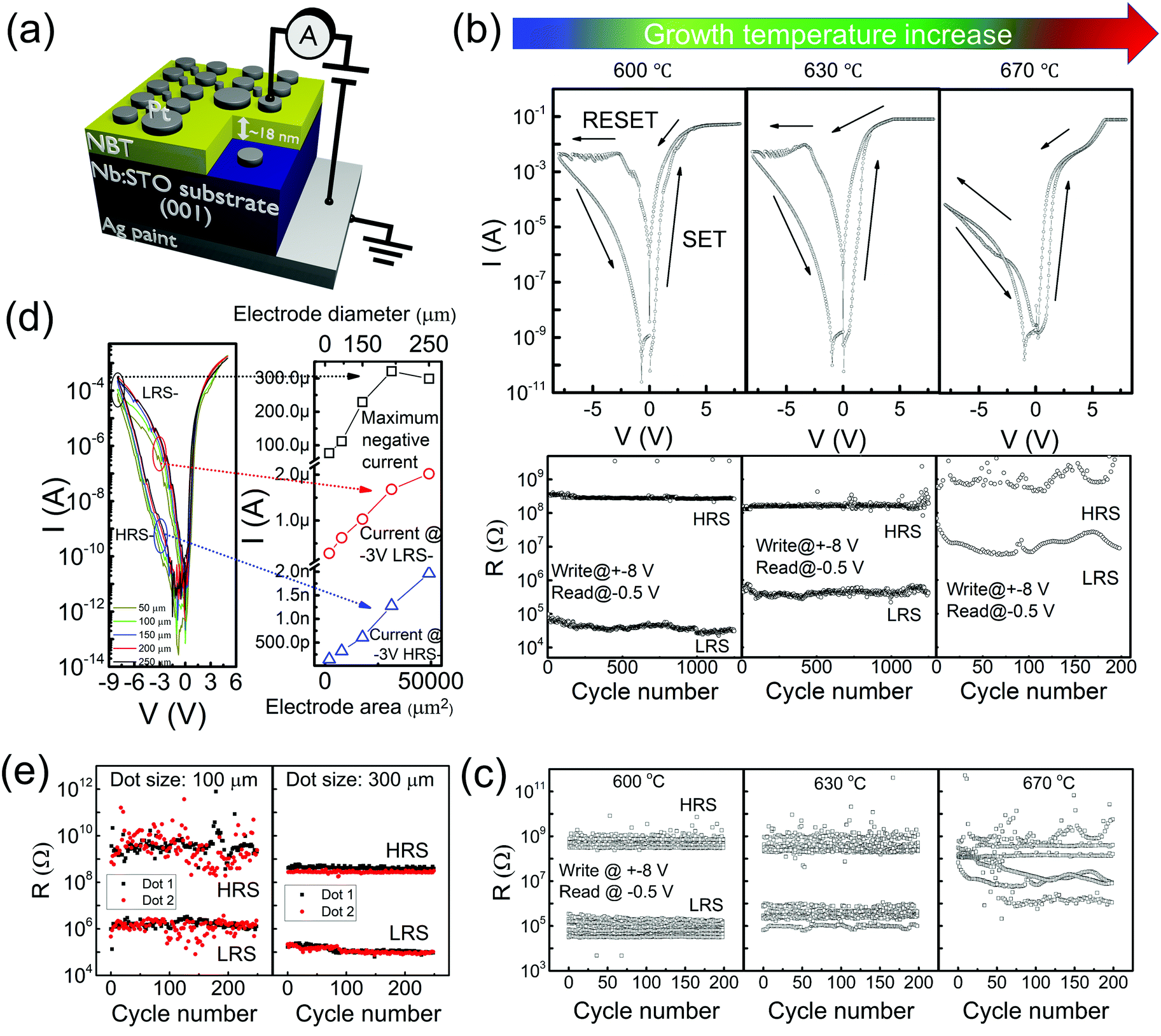 | ||
| Fig. 1 Electrical measurements on the NBT films of this study. (a) Measurement configuration of the Pt/NBT/Nb:STO RS device. (b) Influence of growth temperature on the typical current–voltage (I–V) characteristics of the Pt/NBT/Nb:STO devices (upper panel). Endurance measurements of an individual memory cell on each film: write at ±8 V and read at −0.5 V (lower panel). (c) Influence of growth temperature on the endurance of the devices (write at ±8 V and read at −0.5 V). (d) Influence of electrode size on the I–V curves for Au/NBT/Nb:STO devices, where the NBT was grown at 630 °C. (e) Influence of electrode dot size to the triggered HRS and LRS for the NBT sample grown at 600 °C. | ||
The endurance on the same samples were measured (for 200 cycles) over many different cells (>10) using the same voltage as in Fig. 1b. The results are shown in Fig. 1c. First, we notice that the number of memory cells where uniform readout resistance states are observed without any failure, decreases from 9 to 7 to 3 with increasing growth temperature from 600 to 670 °C. We observe that the absolute resistance values are spaced much more tightly for each memory cell for the lower growth temperatures. Furthermore, they show less variation between different cells. Hence, the films grown at lower temperatures show much more uniform resistive switching. This is confirmed by Fig. S2 (ESI†), which shows the increased standard deviation in the statistical average of the HRS and LRS values with increasing growth temperature. Also, the average ON/OFF ratio decreases from 5000 to 3000 and then to 20 (the largest ON/OFF ratio decreases from 11![[thin space (1/6-em)]](https://www.rsc.org/images/entities/char_2009.gif) 000 to 6000 and then to 100) in these three samples with the increase of the growth temperature.
000 to 6000 and then to 100) in these three samples with the increase of the growth temperature.
The retention properties of the films grown at 600 and 630 °C are shown in Fig. S3A and B (ESI†). An ON/OFF ratio of >103 is maintained even after 2000 s (20000 read cycles), despite a slight degradation of the triggered HRS and LRS. Fig. S4 (ESI†) shows the current response of the NBT sample grown at 630 °C to voltage pulses, where the instantaneous current responds fast to the applied voltage pulse and a fast switching speed is exhibited (butterfly I–V curve still appears for pulse width down to 20 ns and rise time down to 200 ns).
R HRS changes little with deposition temperature of the resistive NBT layer (Fig. 1c) with values of around 108–109 Ω. However, RLRS changes drastically with deposition temperature (from 104 to 107 Ω when the growth temperature increases from 600 to 670 °C) which therefore controls the magnitude of the ON/OFF ratio. The reason for this strong influence of the deposition temperature on RLRS is explored more later.
Fig. 1d show the I–V curves taken from memory cells with different electrode sizes (with diameters of 50, 100, 150, 200, and 250 μm) for an NBT film grown at 630 °C with e-beam evaporated Pt top electrodes. We observe similar shapes of the I–V curves when sputtered Pt is used as the top electrodes (Fig. 1b), indicating little influence of the deposition technique of the top electrodes on the overall RS properties of the devices. A clear linear increase in the measured current (at maximum negative voltage −8 V, LRS and HRS taken at −3 V) with the electrode area indicates a very uniform distribution of the electronic conduction throughout the whole electrode area in both the HRS and LRS. The dependence of electrode area on the RHRS and RLRS of the sample grown at 600 °C using pulsed voltages is shown in Fig. 1e. The average RHRS and RLRS values of the 300 μm electrodes are around nine times as high as those of the 100 μm electrodes, which is consistent with the area ratio of the two electrodes. These observations all suggest that the current conduction of the Pt/NBT/Nb:STO/Ag device does not rely on the formation of local conduction filaments but instead on an interfacial effect or a uniform bulk effect. The electrode area dependence of the HRS indicates also that there is a homogeneous electronic conduction background inside the NBT for the HRS or pristine state. The room temperature resistivity of the NBT film measured using a standard in-line four-probe configuration is ≥106 Ω cm, which is at the boundary between semiconductor and insulator behaviour. As discussed above, this low but non-zero level of electronic conduction is important for bringing the pristine resistance of the NBT-based RS device to a suitable range (∼MΩ)53 and to prevent the need of a high-voltage forming process of very high resistance films, while also preventing current losses of low resistance films. As extrapolated from the low-voltage I–V curves in Fig. S5 (ESI†), we have a device resistance ≈106 Ω (film + contact) in the initial state, which is within the suitable resistance range mentioned above. This value eliminates the need to apply a large voltage to ‘electroform’ conducting filaments. Details of the conduction mechanism will be discussed later when we show fitting of the I–V curves with typical conduction mechanisms.
Fig. 1 clearly indicates that highly uniform RS properties of Pt/NBT/Nb:STO/Ag devices can be achieved by use of lower growth temperatures for the NBT films. To exclude the Nb:STO/metal interface contribution on the overall I–V characteristic of the device, we tested Pt/Nb:STO/Ag structures without NBT films (where the Nb:STO was treated using the same conditions for NBT deposition). All the Pt/Nb:STO/Ag devices exhibit similar and minimal I–V hysteresis loop and negligible variation of readout resistances, and Fig. S6 (ESI†) shows the results for one treated at 630 °C as an example. We also measured energy-dispersive X-ray (EDX) spectra for Ag in multiple areas on the samples (including substrates) that had undergone electrical measurements and found no evidence of Ag diffusion into the films or the substrates (Fig. S7 (ESI†)). Therefore, although it has been reported that Ag could diffuse into Nb:STO46 or that Ag/Nb:STO could show RS effects under certain circumstances,47 none of them occur or are relevant to the results observed here and hence the Ag/Nb:STO interface itself has a negligible contribution to the results of Fig. 1 for our growth and measurement conditions. Also, it is noted that our previous work showed an Ohmic contact nature between the Pt and the NBT interface.48 Hence, the contribution from the Pt/NBT top interface to the RS properties of the device can also be excluded and we can conclude that the NBT/Nb:STO interface controls the overall device performance (we review this in more detail later). Since the Nb:STO substrate has a stable structure and composition, it is the variation of the composition and structure of NBT with growth temperature that most likely influence the performance of NBT/Nb:STO junction and therefore dominates the RS behaviour.
As the NBT composition is quite sensitive to the growth temperature (because of the relatively volatile elements Na and Bi49–51), we therefore next study the compositional change of the NBT films with growth temperature. We used X-ray Photoelectron Spectroscopy (XPS) to assess the stoichiometry change of the NBT films as a function of the growth temperature. The ratio of the XPS spectra area between respective elements can qualitatively reflect the relative elemental ratio between different samples.52–54 The detailed plots and fitting of the Na, Bi, Ti and O XPS spectra are shown in Fig. S8 (ESI†). Fig. 2a and b show the Ti 2p3/2vs. Bi 4f7/2 and Na 1s vs. Bi 4f7/2 spectra with normalizing the Ti 2p3/2 and Na 1s spectra intensity to be the same value, respectively. The relative Bi/Ti and Bi/Na ratios show similar decreasing trends with an increase in growth temperature, as plotted in Fig. 2c. This is understandable by considering that Bi is more volatile than Na and Ti. For instance, the volatilization temperature of Na2O is 1132 °C whereas 825 °C for Bi2O3.55 The volatilization of Bi is well known in the growth of films containing Bi, and for BiFeO3 it has been reported that lower growth temperatures (≤700 °C) are important for optimising the Bi stoichiometry.56
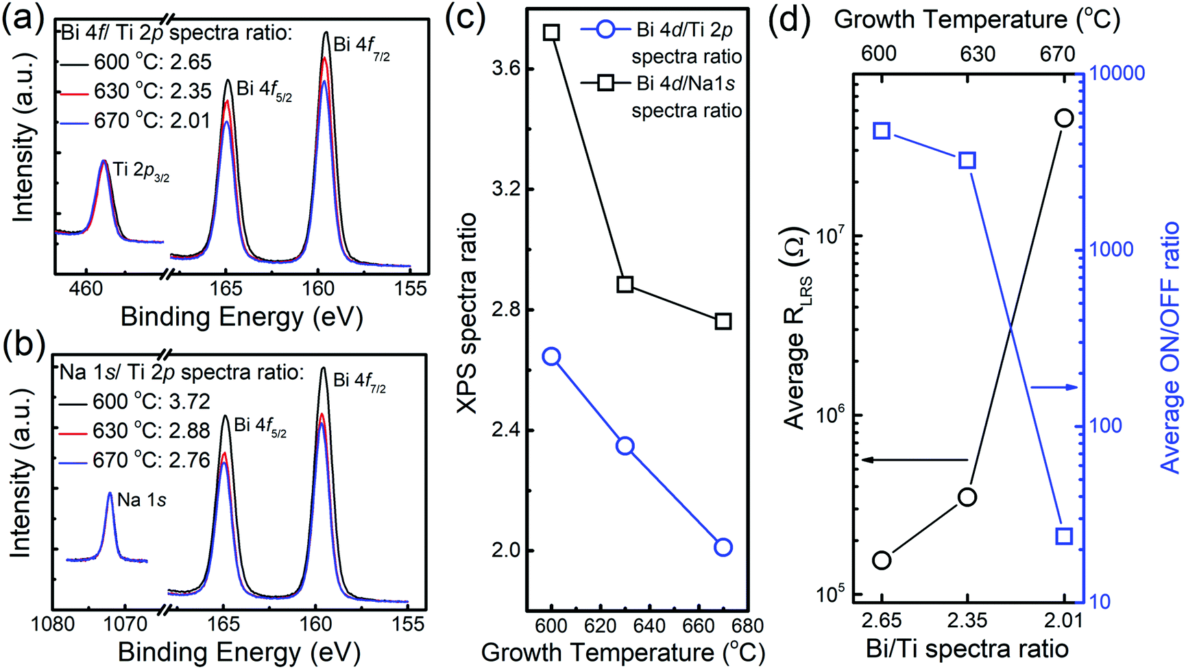 | ||
| Fig. 2 XPS data on the NBT films of this study. (a) Plot of the XPS Bi 4f and Ti 2p3/2 spectra with the Ti 2p3/2 intensity normalized to be the same value. (b) Plot of the XPS Bi 4f and Na 1s spectra with normalising the Na 1s intensity to be the same. (c) XPS spectra area ratio of the Bi 4f7/2vs. Ti 2p3/2 and Bi 4f7/2vs. Na 1s spectra. (d) Plot of the change of Bi/Ti spectra area ratio with average RLRS, ON/OFF ratio. | ||
As shown in Fig. 2d, the relative spectra area of the Bi 4f7/2vs. Ti 2p3/2 (which qualitatively indicates the relative Bi content, assuming negligible Ti loss with increasing growth temperature) shows an inverse relationship with the RLRS and a direct correlation with the ON/OFF ratio. This indicates that the lower the Bi content (i.e. the more loss of Bi) in the film, the worse is the RS performance. The question is how and why the RS performance is related to the Bi content. In fact, it has been reported that slightly Bi-deficient (with x ≤ 0.01 in Na0.5Bi0.5−xTiO3) NBT leads to a fast migration of Vo35,43 whereas more Bi-deficient films result in defect association of Bi vacancies, VBi and Vo, which reduces the concentration of mobile Vo.57,58 We will return to this point later.
Structural analysis was conducted to find out if there is any drastic structural change with varying growth temperature. Fig. 3a shows the XRD 2θ–ω diffraction patterns. All films show clear NBT (00l) peaks with no noticeable peak shift, indicating no obvious structural change with change in growth temperature. Laue fringes are also observed in the film grown at 600 °C, indicating good crystal quality and smooth surfaces. It is also noted that the Laue fringes of Fig. 3a become less clear with an increase of the growth temperature. This indicates that the NBT film is more homogeneous and uniform when the growth temperature is lower. This is very important for potential applications, where the use of low growth temperatures is necessary. Furthermore, the reciprocal space maps (RSMs) of Fig. 3b clearly indicate that the NBT film is fully strained to the STO substrate. The out-of-plane lattice constant is determined to be cNBT = 3.883 ± 0.003 to 3.889 ± 0.003 Å from 2θ–ω scans when the growth temperature increases from 600 to 670 °C, corresponding to 0.56% to 0.41% out-of-plane compressive strain. The slight increase in the lattice constants is consistent with the increase in the off-stoichiometry in perovskite films.59 The out-of-plane compressive strain is consistent with the fact that the bulk lattice constant of NBT (aNBT = 3.886 Å) is smaller than that of STO (aSTO = 3.905 Å), hence the NBT is tensed in-plane by the STO, leading to the out-of-plane compression to conserve the unit-cell volume.
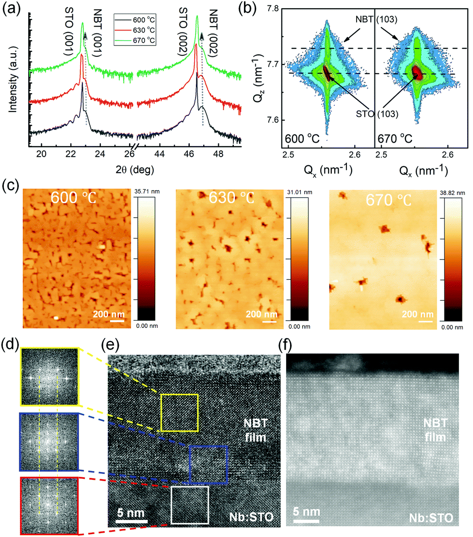 | ||
| Fig. 3 X-ray and microscopy data on the NBT thin films of this study. (a) XRD 2θ–ω diffraction patterns. (b) Reciprocal space maps (RSMs). (c) Atomic force microscopy (AFM) images. (d) Fast Fourier Transformation (FFT) images. (e) Cross-sectional TEM images for film grown at 630 °C. (f) STEM image of the NBT film of (e). | ||
Atomic Force Microscopy (AFM) images shown in Fig. 3c indicate that the surface feature sizes (as measured by the distance between the surface indentations where more than 2 grains meet at a junction) increase rapidly when the growth temperature increases from 600 °C to 630 °C to 670 °C (from ∼100 nm to 200 nm to 500 nm). The increasing grain size is likely related not only to growth temperature,60 but also to the changing film stoichiometry. Indeed, a previous report showed that the grain size in NBT increases with increasing Na/Bi ratio.53 This is consistent with the XPS results (Fig. 2b) showing the increase of Na/Bi ratio with increasing growth temperature. Fig. 3e shows a high-resolution cross-sectional transmission electron microscopy (TEM) image of the NBT film grown at 630 °C, confirming a high-quality epitaxial NBT film on the Nb:STO substrate with a very smooth surface, uniform structure and atomically sharp interface between the film and the substrate. The Fast Fourier Transform (FFT) diffraction patterns shown in Fig. 3d confirm the high-quality epitaxial nature of the film. The STEM image in Fig. 3f further illustrates the overall high film quality.
The above results clearly indicate that the growth temperature in our investigated region strongly influences the stoichiometry of the NBT films without any obvious structural change, except for improved film perfection and homogeneity for the growth at a lower temperature. This is opposite to most perovskite metal oxides which have improved film perfection with an increased growth temperature. The better film perfection at low growth temperatures is linked to the high volatilisation of Na and Bi at high temperatures. With increased growth temperature, on the other hand, the volatility of these elements will lead to cation non-stoichiometry. The 600 °C (the lowest growth temperature in this work) films show the highest ON/OFF ratio with the best device uniformity. The minimum growth temperature of 600 °C that we tried in our work is within the optimum growth temperature (600–650 °C) reported in many works for PLD growth of NBT films48,61,62 (although one study reported a substrate temperature of 550 °C, where they used a lower oxygen pressure during deposition36).
To gain a fundamental understanding of the optimisation of these two properties (ON/OFF ratio and uniformity), it is crucial to first understand the conduction mechanism and then its influence on the RS. Pt is a metal with a high work function (≥5.3 eV63–65). NBT (with Bi loss) has been reported to be a partly compensated p-type semiconductor,42,48,66,67 while Nb:STO is a degenerately doped, highly conductive n-type semiconductor oxide due to its high carrier concentration of 1021 cm−3.68–70 Considering the degenerate semiconductor Nb:STO to be a metal,69,70 the Pt/NBT/Nb:STO sandwich structure consists of two Schottky diodes connected to each other with two Schottky barriers. In the low-bias regime (−1 V to 1 V), the devices show forward rectification (Fig. S6, ESI†), which indicates that the bottom p-type NBT/metal Nb:STO interface has a larger and hence more dominant Schottky barrier height.29,68–71 Therefore, the RS behavior of the device is mainly controlled by the NBT/Nb:STO interface with a simplified band diagram as illustrated in Fig. 4. The depletion layer will be located mainly inside the NBT due to the very high carrier concentration of Nb:STO.72 Considering that the work function of Bi- or Ti- perovskite oxides are usually ≤4.7 eV63,64 while the work function of Nb:STO is around 4.2 eV,73 here the Schottky barrier height should be less than 0.5 eV.
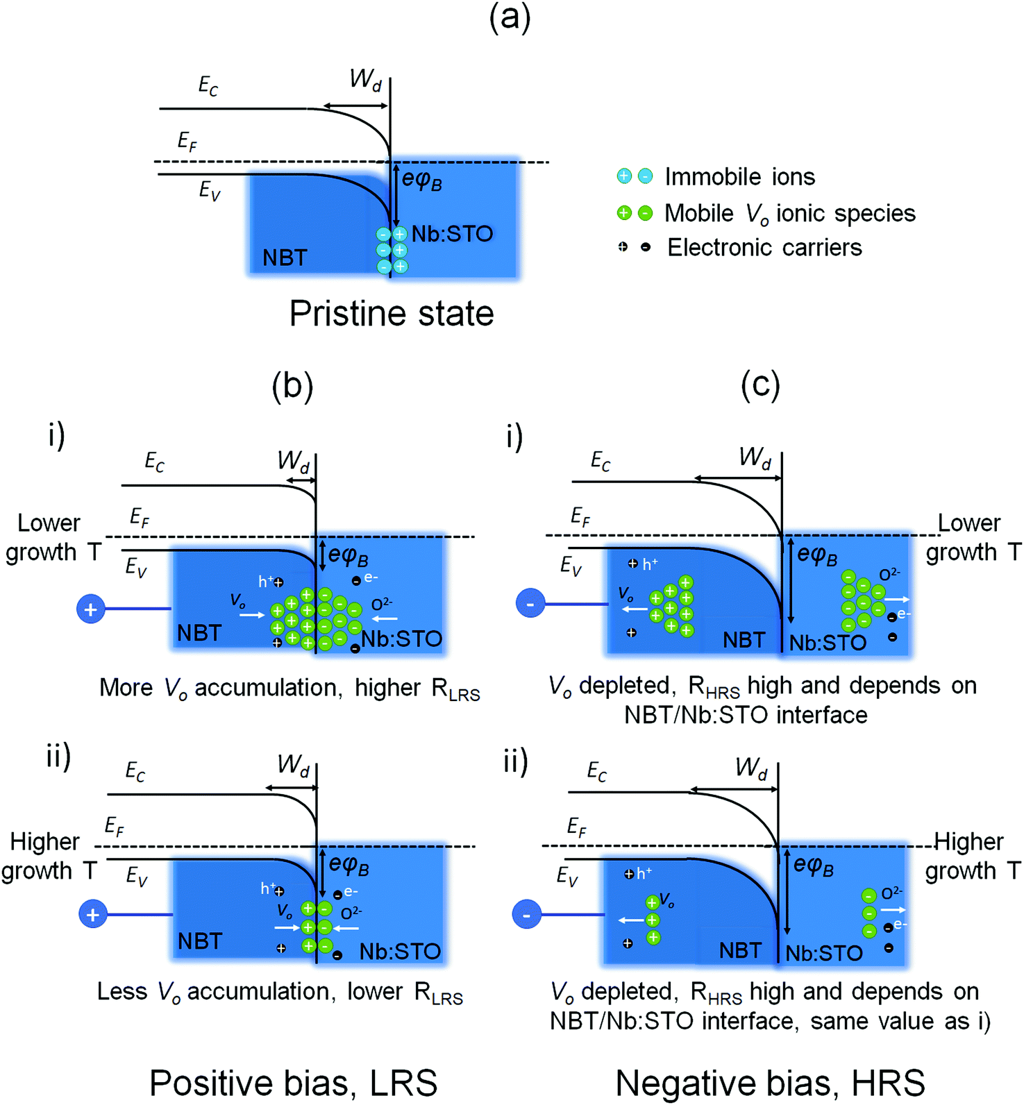 | ||
| Fig. 4 Schematic diagram of the conduction process at the Schottky barrier between NBT film and Nb:STO electrode: (a) the pristine unbiased state. Here EC, EV, EF, Wd and eφB are the conduction band minimum, valence band maximum, Fermi level, depletion layer width, and the Schottky barrier height, respectively. (b) When a positive bias is applied, the interfacial Schottky barrier is reduced, by movement of mobile Vo in the NBT towards the Nb:STO contact, resulting in a LRS. A higher concentration of mobile Vo will lead to a lower LRS value. (c) When a negative bias is applied, the interfacial barrier is increased by movement of mobile Vo in the NBT away from the Nb:STO contact, resulting in a HRS. The HRS is not influenced by the concentration of mobile Vo because the HRS occurs when Vo is depleted from the interface. | ||
Current conduction mechanisms in a metal/semiconductor Schottky contact include emission, tunneling, and/or space charge limited conduction, each with a specified relationship between current density and voltage (electric field).74 We divide the obtained I–V curves into four segments – 1. HRS+: from 0 to +8 V; 2. LRS+: from +8 to 0 V; 3. LRS−: from 0 to −8 V and 4. HRS−: from −8 to 0 V – and fit into different conduction models.
For memristor devices, we are most concerned with low bias regimes. We therefore consider sweeping up from 0 to 0.5 V in segment 1, sweeping down from 1 to 0 V in segment 2, and then sweeping up from 0 to −1 V in segment 3 (in Fig. S9a (ESI†)). A linear fit of log(I) ∼ V1/2 is obtained indicating that interface-limited Schottky emission controls the current conduction in the pristine state. Hence, the intrinsic conduction mechanism is controlled by injection of thermally activated carriers from the electrodes into the conduction band of NBT after overcoming the Schottky barrier by the applied electric field. This is shown in Fig. 4 and discussed below.
Having obtained information about the intrinsic conduction mechanism, we now aim to achieve a clearer picture of the RS process and by doing so, reveal the origin of the switching process and high ON/OFF ratios shown in Fig. 1. As already mentioned, Bi vacancies in the NBT film will give rise to Vo, which is for reasons of charge compensation.35,43,75 The existence of mobile Vo enables the high ionic conductivity in NBT. Fig. S10 (ESI†) shows the normalized ionic conductivity as a function of temperature for the NBT film grown at 600 °C, where a typical Arrhenius-type behaviour is exhibited, indicating that the conductivity of the film is thermally activated with an activation energy Ea = 0.51 eV, consistent with the Ea of optimised ionic conductivity in NBT.35
In the band diagram in Fig. 4a in the non-bias state, for the NBT/Nb:STO junction there is a potential barrier for the majority carriers in NBT (holes) right at the interface between the semiconductor film (NBT) and the metallic substrate (Nb:STO). The barrier height32 can be reduced/increased by an external applied bias, resulting in high/low conduction current. Vos accumulate and/or are depleted near the NBT/Nb:STO interface under an external field. To explain the RS mechanism and the influence of the growth temperature, we consider the migration of mobile Vo near and away from the NBT/Nb:STO interface for controlling the Schottky barrier height and hence the overall RLRS.32
With a positive bias applied to the Pt top electrode (and the Nb:STO is grounded), positively charged Vo in the NBT drift to and accumulate near the NBT/Nb:STO interface, forming a highly positive charge region (Fig. 4b). A negatively charged region is also formed on the Nb:STO side at the same time due to the accumulation of O2− ions.76,77 The increase in Vo concentration near the interface under positive bias, which results in a modified band structure,71 can further reduce the Schottky barrier height/width. This will thus result in a high electronic conduction current and a low RLRS.32 Here, RLRS is highly dependent on the film growth temperature since the concentration of mobile Vo will change with the film composition. A small amount of Bi deficiency (x ≈ −0.01) gives a high Vo concentration (consistent with the NBT film grown at 600 °C).35 As already mentioned, as the growth temperature increases, the Bi vacancy (VBi) concentration increases (Fig. 2). At the same time, the amount of Vo–VBi defect association will increase leading to a reduction in mobile Vo.57,58 This means there will be less migration of Vo to and away from the electrodes, and thus a less effective lowering of the barrier height/width. This then explains why RLRS increases as the film growth temperature increases, and consequently, the ON/OFF ratio decreases.
When the positive SET bias is switched off, the LRS is maintained (Fig. 1b), indicating that the Vo concentration near the interface remains high. When a negative bias is applied, the Vo concentration near the interface is reduced. This Vo depletion near the NBT/Nb:STO interface causes an increase in the Schottky barrier height/width, which leads to a much lower conduction current under negative bias, driving the memory cell to the HRS (Fig. 4c).
As shown in Fig. 4b, RLRS is lower for the 600 °C sample, where the Vo concentration at the interface is higher than for the 670 °C sample (ii), while RHRS is almost the same for the NBT films grown at different temperatures (Fig. 4c) because under negative bias, the Vos are fully depleted from the interface (regardless of the initial Vo concentration, i.e., high for the 600 °C sample) (i) and low for the 670 °C sample (ii). Hence, the ON/OFF ratio will be controlled only by the RLRS in our system, which depends highly on the mobile Vo concentration.
The larger hysteresis of the I–V curves of Fig. 1b under negative bias compared to positive bias can be explained by the different influences of the SET and RESET processes on Vo concentration: under a positive bias, Vo contributes to the shrinkage of the depletion layer width which dominates the current conduction. After the SET process, the current drop generates a small hysteresis due to the remaining accumulation of the Vo near the NBT/Nb:STO interface. On the other hand, under negative bias after the RESET process, the Vos are fully depleted and hence the Vos cannot modulate the depletion layer width and so the change in the Schottky barrier height takes over to dominate the current conduction. Hence, the resistive behavior will be quite different compared to the positive bias region. Also, the whole system should now become quite insulating due to the depletion of Vo which is reflected by the self-compliance or deep RESET of the current78 (with nearly negative differential current dI/dV on negative side of Fig. 1b at 600 °C). Thus, the current will drop dramatically when the negative bias is decreasing, generating a larger hysteresis.
To prove the role of Schottky barrier height on the RS behaviour, from Fig. S10 (ESI†) and with relevant parameters listed in Table S1 (ESI†), we study the zero-bias barrier heights at different resistance states. The zero-bias Schottky barrier height in the initial state or HRS (eφB0H) has almost the same value regardless of growth temperature of the film, while the non-bias Schottky barrier height in the LRS (eφB0L) decreases with decreasing growth temperature and is closely linked with the RLRS. These results are consistent with the RHRS (Vo depleted state near the NBT/Nb:STO interface) being high and almost constant with growth temperature and RLRS (Vo accumulated after the SET process) decreasing with decreasing growth temperature when a higher concentration of mobile Vos accumulate near the NBT/Nb:STO interface at positive bias, causing a lower Schottky barrier height.
Conclusions
Single-phase epitaxial ionic Na0.5Bi0.5TiO3 (NBT) films grown under different conditions were used to demonstrate that high Vo concentration and a low-level electronic conduction are critical features for forming-free memristors with a high ON/OFF ratio, stable switching, and good endurance/retention via interfacial Schottky barrier-controlled switching. This material system is unique among perovskites in that low growth temperatures can be used to grow very thin films with high homogeneity, high uniformity and low leakage. This is very different to other widely studied perovskites for memristors. Since NBT can be grown by a variety of physical vapour deposition processes at relatively low temperatures, this makes it a promising, industry-relevant material system for memristors and neuromorphic computing applications.Experimental section
Sample preparation
Na0.5Bi0.5TiO3 films were grown on single crystalline 0.5% wt Nb-doped SrTiO3(001) substrates using pulsed laser deposition (PLD). The composite PLD target was prepared using a conventional solid-state sintering: stoichiometric and high-purity Na2CO3 (99.99%), Bi2O3 (99.99%, 10% excess), TiO2 (99.99%) powders were mixed, ground, and then being sintered at 850 °C for 2 h, then re-ground again and pelletized, followed by additional sintering at 1100 °C for 3 h. During PLD, the oxygen partial pressure was maintained at 0.3 mbar and the growth temperature was varied from 600 to 670 °C. The substrate temperature was measured using an infrared pyrometer. A KrF excimer laser with a 248 nm wavelength was used. The repetition rate and laser fluency were 1 Hz and 1.5 J cm−2, respectively.Sample characterization
The phase and crystallinity of the films were characterized with a Panalytical Empyrean high-resolution X-ray diffraction (XRD) system using Cu-Kα radiation (λ = 1.5405 Å). Cross-sectional images of the film were obtained by high-resolution transmission electron microscopy (HRTEM) FEI TALOS F200X at 200 kV equipped with ultrahigh-resolution high angle annular dark field detectors and Super-XTM electron-dispersive X-ray spectroscopy. Both cross-sectional TEM and scanning TEM (STEM) were undertaken. The samples for the TEM analyses were obtained through mechanical grinding, dimpling, and a final ion milling step. For characterization of the electrical properties, platinum electrodes were deposited by DC sputtering or e-beam evaporation. We measured the resistances using a Signatone two-probe station with a Tungsten tip (25 μm) and a Keithley 2400 source-meter. To measure ionic transport characteristics, we used an HP 4294A Precision Impedance Analyser. For all measurements, Nb-doped STO substrates were grounded and the voltage was applied to the Pt electrodes. X-ray photoelectron spectroscopy (XPS) was used to study the valence band of the films by a monochromatic Al Kα1 X-ray source (hν = 1486.6 eV) using a SPECS PHOIBOS 150 electron energy analyzer with a total energy resolution of 500 meV. The Fermi level of the films was calibrated by a polycrystalline Au foil.Author contributions
C. Y. and J. L. M.-D. conceived the ideas. C. Y., M. W. and R. W. made the samples. C. Y. carried out XRD and AFM characterization. C. Y., M. W., R. W., M. X., M. H. and S. D. conducted the electrical properties measurements. W. L. carried out XPS measurement, and J. S., K. H. L. Z. contributed to the XPS data analysis. H. D., X. G., D. Z. and H. Y. W. performed TEM imaging. C. Y., J. L. M.-D., A. K., A. C. and Q. J. contributed to data analysis. C. Y., J. L. M.-D. and Q. J. wrote the manuscript. All authors contributed to reviewing the data in this manuscript and commenting on the manuscript.Conflicts of interest
There are no conflicts to declare.Acknowledgements
The Cambridge investigators acknowledge funding from Royal Academy of Engineering – CIET1819_24, the Leverhulme Trust grant RPG-2015-017, EPSRC grants EP/N004272/1, EP/T012218/1, EP/P007767/1, and EP/M000524/1, the Isaac Newton Trust in Cambridge (minute 16.24(p) and RG96474). The US–UK collaborative effort in U.S. was funded by the U.S. National Science Foundation (ECCS-1902644 (Purdue University)), ECCS-1902623 (University at Buffalo, SUNY). The work at Los Alamos National Laboratory was supported by the NNSA's Laboratory Directed Research and Development Program and was performed, in part, at the Center for Integrated Nanotechnologies, an Office of Science User Facility operated for the U.S. Department of Energy Office of Science. Los Alamos National Laboratory, an affirmative action equal opportunity employer, is managed by Triad National Security, LLC for the U.S. Department of Energy's NNSA, under Contract No. 89233218CNA000001.Notes and references
- G. I. Meijer, Science, 2008, 319, 1625–1626 CrossRef CAS PubMed.
- J. Meena, S. Sze, U. Chand and T.-Y. Tseng, Nanoscale Res. Lett., 2014, 9, 526 CrossRef PubMed.
- W. Li, J. Shi, K. H. L. Zhang and J. L. MacManus-Driscoll, Mater. Horiz., 2020, 7, 2832–2859 RSC.
- R. Waser, R. Dittmann, G. Staikov and K. Szot, Adv. Mater., 2009, 21, 2632–2663 CrossRef CAS.
- A. Sawa, Mater. Today, 2008, 11, 28–36 CrossRef CAS.
- C. Hu, M. D. McDaniel, J. G. Ekerdt and E. T. Yu, IEEE Electron Device Lett., 2013, 34, 1385–1387 CAS.
- A. Prakash, D. Jana and S. Maikap, Nanoscale Res. Lett., 2013, 8, 1–17 CrossRef PubMed.
- T. Tan, Y. Du, A. Cao, Y. Sun, H. Zhang and G. Zha, RSC Adv., 2018, 8, 41884–41891 RSC.
- K. L. Lin, T. H. Hou, J. Shieh, J. H. Lin, C. T. Chou and Y. J. Lee, J. Appl. Phys., 2011, 109, 1–7 Search PubMed.
- J. Guo, X. Kang, Y. Gao, W. Chen and X. Zhao, Appl. Phys. Lett., 2018, 113(4), 04352 CrossRef.
- S. Yu, H. Y. Chen, B. Gao, J. Kang and H. S. P. Wong, ACS Nano, 2013, 7, 2320–2325 CrossRef CAS PubMed.
- J. Joshua Yang, F. Miao, M. D. Pickett, D. A. A. Ohlberg, D. R. Stewart, C. N. Lau and R. S. Williams, Nanotechnology, 2009, 20, 215201 CrossRef CAS PubMed.
- S. Bagdzevicius, K. Maas, M. Boudard and M. Burriel, J. Electroceram., 2017, 39, 157–184 CrossRef CAS.
- Y. B. Zhu, K. Zheng, X. Wu and L. K. Ang, Sci. Rep., 2017, 7, 43664 CrossRef CAS PubMed.
- Z. B. Yan and J.-M. Liu, Ann. Phys., 2015, 358, 206–224 CAS.
- A. Chen, W. Zhang, L. R. Dedon, D. Chen, F. Khatkhatay, J. L. MacManus-Driscoll, H. Wang, D. Yarotski, J. Chen, X. Gao, L. W. Martin, A. Roelofs and Q. Jia, Adv. Funct. Mater., 2020, 2000664 CrossRef CAS.
- G. Sassine, S. La Barbera, N. Najjari, M. Minvielle, C. Dubourdieu and F. Alibart, J. Vac. Sci. Technol., B: Nanotechnol. Microelectron.: Mater., Process., Meas., Phenom., 2016, 34, 012202 Search PubMed.
- H. Y. Jeong, J. Y. Lee and S.-Y. Choi, Adv. Funct. Mater., 2010, 20, 3912–3917 CrossRef CAS.
- H. Y. Jeong, J. Y. Lee, M.-K. Ryu and S.-Y. Choi, Phys. Status Solidi RRL, 2010, 4, 28–30 CrossRef CAS.
- S. Spiga, A. Lamperti, C. Wiemer, M. Perego, E. Cianci, G. Tallarida, H. L. Lu, M. Alia, F. G. Volpe and M. Fanciulli, Microelectron. Eng., 2008, 85, 2414–2419 CrossRef CAS.
- P. Basnet, D. G. Pahinkar, M. P. West, C. J. Perini, S. Graham and E. M. Vogel, J. Mater. Chem. C, 2020, 8, 5092–5101 RSC.
- Y. Sun, X. Yan, X. Zheng, Y. Liu, Y. Zhao, Y. Shen, Q. Liao and Y. Zhang, ACS Appl. Mater. Interfaces, 2015, 7, 7382–7388 CrossRef CAS PubMed.
- M. Ismail, S.-U. Nisa, A. M. Rana, T. Akbar, J. Lee and S. Kim, Appl. Phys. Lett., 2019, 114, 012101 CrossRef.
- S. Wu, X. Luo, S. Turner, H. Peng, W. Lin, J. Ding, A. David, B. Wang, G. Van Tendeloo, J. Wang and T. Wu, Phys. Rev. X, 2013, 3, 041027 CAS.
- K. C. Sekhar, J. P. B. Silva, K. Kamakshi, M. Pereira and M. J. M. Gomes, Appl. Phys. Lett., 2013, 102, 212903 CrossRef.
- M. Y. Song, Y. Seo, Y. S. Kim, H. D. Kim, H.-M. An, B. H. Park, Y. M. Sung and T. G. Kim, Appl. Phys. Express, 2012, 5, 091202 CrossRef.
- S.-S. Li and Y.-K. Su, RSC Adv., 2019, 9, 2941–2947 RSC.
- W. Dai, Y. Li, C. Jia, C. Kang, M. Li and W. Zhang, RSC Adv., 2020, 10, 18039–18043 RSC.
- Y. Cui, H. Peng, S. Wu, R. Wang and T. Wu, ACS Appl. Mater. Interfaces, 2013, 5, 1213–1217 CrossRef CAS PubMed.
- M. Zhao, Y. Zhu, M. Li, Y. Zhang, X. Tan, C. Hu, Q. Wang, F. Zhang, S. Pu and R. Xiong, J. Phys. D: Appl. Phys., 2017, 50, 265102 CrossRef.
- S. M. Yang, S. Lee, J. Jian, W. Zhang, P. Lu, Q. Jia, H. Wang, T. Won Noh, S. V. Kalinin and J. L. MacManus-Driscoll, Nat. Commun., 2015, 6, 8588 CrossRef CAS PubMed.
- S. Cho, C. Yun, S. Tappertzhofen, A. Kursumovic, S. Lee, P. Lu, Q. Jia, M. Fan, J. Jian, H. Wang, S. Hofmann and J. L. MacManus-Driscoll, Nat. Commun., 2016, 7, 12373 CrossRef CAS PubMed.
- M.-T. Chentir, E. Bouyssou, L. Ventura and C. Anceau, J. Appl. Phys., 2009, 105, 061605 CrossRef.
- B. Chen, H. Yang, J. Miao, L. Zhao, L. X. Cao, B. Xu, X. G. Qiu and B. R. Zhao, J. Appl. Phys., 2005, 97, 024106 CrossRef.
- M. Li, M. J. Pietrowski, R. A. De Souza, H. Zhang, I. M. Reaney, S. N. Cook, J. A. Kilner and D. C. Sinclair, Nat. Mater., 2014, 13, 31–35 CrossRef CAS.
- J. Song, J. Gao, S. Zhang, L. Luo, X. Dai, L. Zhao and B. Liu, Crystals, 2019, 9, 558 CrossRef CAS.
- S. Rehman, H. Kim, M. Farooq Khan, J.-H. Hur, A. D. Lee and D. Kim, Sci. Rep., 2019, 9, 19387 CrossRef CAS.
- D. Bhatnagar, A. Kumar, K. Prabahar, M. Suri, A. Srinivas and R. Chatterjee, Appl. Phys. Lett., 2018, 113, 162101 CrossRef.
- D. Filatov, D. Antonov, I. Antonov, A. Kasatkin and O. Gorshkov, J. Mater. Sci. Chem. Eng., 2017, 05, 8–14 CAS.
- D. O. Filatov, M. N. Koriazhkina, D. A. Antonov, I. N. Antonov, D. A. Liskin, M. A. Ryabova and O. N. Gorshkov, IOP Conf. Ser. Mater. Sci. Eng., 2019, 699, 012012 CrossRef CAS.
- G. Geneste, C. Paillard and B. Dkhil, Phys. Rev. B, 2019, 99, 024104 CrossRef CAS.
- F. Yang, M. Li, L. Li, P. Wu, E. Pradal-Velázquez and D. C. Sinclair, J. Mater. Chem. A, 2018, 6, 5243–5254 RSC.
- F. Yang, M. Li, L. Li, P. Wu, E. Pradal-Velázque and D. C. Sinclair, J. Mater. Chem. A, 2017, 5, 21658–21662 RSC.
- L. Zhang, S. Cosemans, D. J. Wouters, G. Groeseneken, M. Jurczak and B. Govoreanu, IEEE Electron Device Lett., 2015, 36, 570–572 CAS.
- Z. C. Wang, J. Miao, P. F. Liu, Y. Ji, F. Shao, K. K. Meng, J. Teng, Y. Wu, X. G. Xu and Y. Jiang, J. Mater. Sci.: Mater. Electron., 2017, 28, 12816–12822 CrossRef CAS.
- Y. Cui, L. Zhang, R. Wang and J. Qian, Mater. Sci. Eng., B, 2007, 138, 214–218 CrossRef CAS.
- X. G. Chen, X. B. Ma, Y. B. Yang, L. P. Chen, G. C. Xiong, G. J. Lian, Y. C. Yang and J. B. Yang, Appl. Phys. Lett., 2011, 98, 122102 CrossRef.
- R. Wu, A. Kursumovic, X. Gao, C. Yun, M. E. Vickers, H. Wang, S. Cho and J. L. MacManus-Driscoll, ACS Appl. Mater. Interfaces, 2018, 10, 18237–18245 CrossRef CAS PubMed.
- T. Rojac, A. Bencan, B. Malic, G. Tutuncu, J. L. Jones, J. E. Daniels and D. Damjanovic, J. Am. Ceram. Soc., 2014, 97, 1993–2011 CrossRef CAS.
- M. Tomczyk, D. G. Stroppa, I. M. Reaney and P. M. Vilarinho, Phys. Chem. Chem. Phys., 2017, 19, 14337–14344 RSC.
- H. Zhang, A. H. H. Ramadan and R. A. De Souza, J. Mater. Chem. A, 2018, 6, 9116–9123 RSC.
- X. C. Huang, J. Y. Zhang, M. Wu, S. Zhang, H. Y. Xiao, W. Q. Han, T.-L. Lee, A. Tadich, D.-C. Qi, L. Qiao, L. Chen and K. H. L. Zhang, Phys. Rev. B, 2019, 100, 115301 CrossRef CAS.
- P. Singh, P. K. Jha, A. S. K. Sinha, P. A. Jha and P. Singh, Solid State Ionics, 2020, 345, 115158 CrossRef CAS.
- T. Tan, Y. Du, A. Cao, Y. Sun, H. Zhang and G. Zha, RSC Adv., 2018, 8, 41884–41891 RSC.
- M. Höfling, S. Steiner, A.-P. Hoang, I.-T. Seo and T. Frömling, J. Mater. Chem. C, 2018, 6, 4769–4776 RSC.
- V. Shelke, V. N. Harshan, S. Kotru and A. Gupta, J. Appl. Phys., 2009, 106, 104114 CrossRef.
- L. Koch, S. Steiner, K.-C. Meyer, I.-T. Seo, K. Albe and T. Frömling, J. Mater. Chem. C, 2017, 5, 8958–8965 RSC.
- K.-C. Meyer and K. Albe, J. Mater. Chem. A, 2017, 5, 4368–4375 RSC.
- C. M. Brooks, L. F. Kourkoutis, T. Heeg, J. Schubert, D. A. Muller and D. G. Schlom, Appl. Phys. Lett., 2009, 94, 162905 CrossRef.
- K. S. Ojha, Ferroelectrics, 2015, 474, 163–168 CrossRef CAS.
- A. S. Daryapurkar, J. T. Kolte, P. R. Apte and P. Gopalan, Crystals, 2019, 9, 558 CrossRef.
- A. S. Daryapurkar, J. T. Kolte and P. Gopalan, Ferroelectrics, 2013, 447, 46–55 CrossRef CAS.
- J. Robertson and C. W. Chen, Appl. Phys. Lett., 1999, 74, 1168–1170 CrossRef CAS.
- T. You, X. Ou, G. Niu, F. Bärwolf, G. Li, N. Du, D. Bürger, I. Skorupa, Q. Jia, W. Yu, X. Wang, O. G. Schmidt and H. Schmidt, Sci. Rep., 2015, 5, 18623 CrossRef CAS PubMed.
- D. Gu, S. K. Dey and P. Majhi, Appl. Phys. Lett., 2006, 89, 082907 CrossRef.
- C. H. Yang, W. B. Wu, F. Yang, H. T. Wu and X. Y. Zhang, Mater. Lett., 2012, 66, 86–88 CrossRef CAS.
- H. Peng, J. Kui-Juan, L. Hui-Bin, J. Jin-Feng, Q. Jie, H. Chun-Lian and Y. Guo-Zhen, Chin. Phys. Lett., 2009, 26, 027301 CrossRef.
- A. Bera, H. Peng, J. Lourembam, Y. Shen, X. W. Sun and T. Wu, Adv. Funct. Mater., 2013, 23, 4977–4984 CrossRef CAS.
- C. H. Jia, X. W. Sun, G. Q. Li, Y. H. Chen and W. F. Zhang, Appl. Phys. Lett., 2014, 104, 043501 CrossRef.
- Z. Luo, L. Pei, M. Li, Y. Zhu, S. Xie, X. Cheng, J. Liu, H. Ding and R. Xiong, Appl. Phys. Lett., 2018, 112, 153504 CrossRef.
- M. Vagadia, A. Ravalia, P. S. Solanki, R. J. Choudhary, D. M. Phase and D. G. Kuberkar, Appl. Phys. Lett., 2013, 103, 033504 CrossRef.
- Y. Nam, I. Hwang, S. Oh, S. Lee, K. Lee, S. Hong, J. Kim, T. Choi and B. Ho Park, Appl. Phys. Lett., 2013, 102, 162105 CrossRef.
- B. Nagaraj, T. Wu, S. B. Ogale, T. Venkatesan and R. Ramesh, J. Electroceram., 2002, 8, 233–241 CrossRef CAS.
- F.-C. Chiu, Adv. Mater. Sci. Eng., 2014, 2014, 1–18 Search PubMed.
- J. L. MacManus-Driscoll, M. P. Wells, C. Yun, J.-W. Lee, C.-B. Eom and D. G. Schlom, APL Mater., 2020, 8, 040904 CrossRef CAS.
- K. Zheng, X. W. Sun and K. L. Teo, Nanosci. Nanotechnol. Lett., 2013, 5, 868–871 CrossRef CAS.
- K. Zheng, J. L. Zhao, X. W. Sun, V. Q. Vinh, K. S. Leck, R. Zhao, Y. G. Yeo, L. T. Law and K. L. Teo, Appl. Phys. Lett., 2012, 101, 143110 CrossRef.
- J. Liu, H. Yang, Y. Ji, Z. Ma, K. Chen, X. Zhang, H. Zhang, Y. Sun, X. Huang and S. Oda, Nanotechnology, 2018, 29, 415205 CrossRef.
Footnote |
| † Electronic supplementary information (ESI) available: I–V curve for the 1st cycle and afterwards repetitions, distribution of RLRS and RHRS, retention property of the Pt/NBT/Nb:STO resistive switching devices, switching speed and current response under voltage pulses, current vs. voltage measurement of the Pt/Nb:STO/Ag sample, evidence of absence of Ag diffusion in the NBT/Nb:STO/Ag samples, analysis on the relative stoichiometric change of the NBT samples using XPS, analysis of conduction mechanism by I–V fitting, ionic conductivity of the NBT film. See DOI: 10.1039/d1tc00202c |
| This journal is © The Royal Society of Chemistry 2021 |