
 Open Access Article
 This Open Access Article is licensed under a Creative Commons Attribution-Non Commercial 3.0 Unported Licence
N-Doping improves charge transport and morphology in the organic non-fullerene acceptor O-IDTBR†
Alexandra F.
Paterson
 *ab,
Ruipeng
Li
c,
Anastasia
Markina
d,
Leonidas
Tsetseris
e,
Sky
MacPhee
b,
Hendrik
Faber
b,
Abdul-Hamid
Emwas
f,
Julianna
Panidi
g,
Helen
Bristow
h,
Andrew
Wadsworth
h,
Derya
Baran
b,
Denis
Andrienko
d,
Martin
Heeney
g,
Iain
McCulloch
bh and
Thomas D.
Anthopoulos
*b
*ab,
Ruipeng
Li
c,
Anastasia
Markina
d,
Leonidas
Tsetseris
e,
Sky
MacPhee
b,
Hendrik
Faber
b,
Abdul-Hamid
Emwas
f,
Julianna
Panidi
g,
Helen
Bristow
h,
Andrew
Wadsworth
h,
Derya
Baran
b,
Denis
Andrienko
d,
Martin
Heeney
g,
Iain
McCulloch
bh and
Thomas D.
Anthopoulos
*b
aDepartment of Chemical and Materials Engineering, and Centre for Applied Energy Research, University of Kentucky, Lexington, Kentucky 40506, USA. E-mail: alexandra.paterson@uky.edu
bKing Abdullah University of Science and Technology, KAUST Solar Centre, Thuwal, 23955-6900, Saudi Arabia
cNational Synchrotron Light Source II (NSLS II), Brookhaven National Lab, Upton, New York, USA
dMax Planck Institute for Polymer Research, Ackermannweg 10, 55128 Mainz, Germany
eDepartment of Physics, National Technical University of Athens, Athens GR-15780, Greece
fCore Labs, King Abdullah University of Science and Technology, Thuwal 23955-6900, Saudi Arabia
gDepartment of Chemistry and Centre for Plastic Electronics, Imperial College London, South Kensington, London SW7 2AZ, UK
hDepartment of Chemistry, Chemistry Research Laboratory, University of Oxford, Oxford OX1 3TA, UK
First published on 10th March 2021
Abstract
Molecular doping has been shown to improve the performance of various organic (opto)electronic devices. When compared to p-doped systems, research into n-doped organic small-molecules is relatively limited, primarily due to the lack of suitable dopants and the often encountered unfavourable microstructural effects. These factors have prevented the use of n-doping in a wider range of existing materials, such as non-fullerene acceptors (NFAs), that have already shown great promise for a range of (opto)electronic applications. Here, we show that several different molecular n-dopants, namely [1,2-b:2′,1′-d]benzo[i][2.5]benzodiazocine potassium triflate adduct (DMBI-BDZC), tetra-n-butylammonium fluoride (TBAF) and 4-(2,3-dihydro-1,3-dimethyl-1H-benzimidazol-2-yl)-N,N-dimethylbenzenamine (N-DMBI), can be used to n-dope the molecular semiconductor O-IDTBR, a promising NFA, and increase the electron field-effect mobility to >1 cm2 V−1 s−1. By combining complementary experimental techniques with computer simulations of doping and charge carrier dynamics, we show that improved charge transport arises from synergistic effects of n-type doping and morphological changes. Specifically, a new, previously unreported dopant-induced packing orientation results in one of the highest electron mobility values reported to-date for an NFA molecule. Overall, this work highlights the importance of dopant–semiconductor interactions and their impact on morphology, showing that dopant-induced molecular packing motifs may be generic and a key element of the charge transport enhancement observed in doped organics.
Introduction
Electronic doping is an established technique throughout the semiconductor industry. Specifically: carefully selecting and incorporating an additional material into a host semiconductor to induce (or remove) electrons allows for the accurate control of the charge transport in the semiconductor.1–3 This, in turn, can have enormous impact on the key performance metrics in a broad range of electronic devices: from incumbent inorganic semiconductors to emergent organic semiconductors (OSCs), and their application in transistors, solar cells, photodetectors, and light emitting diodes. For example, in organic thin-film transistors (OTFTs), molecular doping has been shown to greatly improve all operating characteristics.4,5Yet despite the clear evidence that doping has extreme beneficial qualities, to-date, there remain a few key categories of semiconductor that have been explored significantly less than others. For example, in OSCs, doping has been widely explored in hole transporting (p-type) polymers; on the other hand, investigation into doped electron transporting (n-type) small-molecules remains scarce. Reasons for this include: (i) the requirement for extreme energetics that lead to unstable n-type dopants,3 and (ii) low doping efficiencies due to limited solubility/miscibility.2,6–8 The former makes it extremely difficult to identify materials that act as n-type dopants,7 whereas the latter can result in structural defects with adverse effects on charge transport – especially in highly crystalline small-molecule OSCs.6,9 This is particularly the case for solution-processed small-molecules: final layer-morphology is governed by complex interactions between processing conditions, such as solvent-drying kinetics, and nucleation and growth processes. The introduction of an additional component (dopant) and its coupling to the host semiconductor can significantly alter such mechanisms, thereby impacting the final layer microstructure.
However, recent studies suggest the presence of dopant molecules does not necessarily have a detrimental impact on OSC morphology. Indeed, Jacobs and Moulé noted that the strong coupling between solubility, doping and morphology could instead be exploited to pattern OSCs and control crystallinity.2 This is further supported by the fact that Lewis acids, such as B(C6F5)3 and Zn(C6F5)2, have recently been shown to play the role of both molecular dopant and morphology modifiers.10,11 Along with the steady growth in the library of n-type molecular dopants,12–14 these latest observations are important for solution-processed n-type small-molecules – especially for those that have already shown to be exceptional OSCs for various applications. For example, materials such as non-fullerene acceptors (NFAs) have received great interest in recent years in the field of organic photovoltaics (OPVs). Their role in achieving record OPV efficiencies (>15%) arises from a number of inherent, desirable NFA-characteristics,15 including synthetically tuneable optical properties, improved long-term morphological stability and high charge carrier mobility, μ.16 In terms of the latter property, one such NFA, O-IDTBR, has shown a superior structure/packing motif as compared to other NFAs, leading to impressive μe ≈ 0.12 cm2 V−1 s−1 measured in OTFTs.17 If n-doping were to further enhance the charge transport of O-IDTBR, it would be of significant and broad interest to the organic electronics community, with relevance to solar cells, photodetectors and transistors.
Here, we use thin-film transistors and computer simulations of doping and charge dynamics, to investigate the impact of n-doping on the transport characteristics of solution-processed O-IDTBR. We use two relatively unexplored molecular n-type dopants, [1,2-b:2′,1′-d]benzo[i][2.5]benzodiazocine potassium triflate adduct (DMBI-BDZC) and tetra-n-butylammonium fluoride (TBAF), and one well-known molecular n-type dopant N,N-dimethylbenzenamine (N-DMBI). We find that one of the most striking effects from the simple, solution-phase admixing of each dopant, is the significant increase in electron mobility, reaching values in excess of 1 cm2 V−1 s−1 with all n-dopants: the highest reported electron mobility for an NFA small-molecule to-date, and the first example of exploiting molecular doping for enhancing the carrier transport in NFA-based transistor. Electron paramagnetic resonance (EPR) spectroscopy and transistor measurements suggest the improvement in mobility arises from successful n-type doping, atomic force microscopy and grazing incidence wide-angle X-ray scattering suggest the dopants also act as additives that affect the layer morphology. Furthermore, microstructural analysis via X-ray diffraction (XRD) measurements uncovers a previously unidentified O-IDTBR orientation/packing motif, with preferential in-plane π-stacking, in the optimally doped systems. Theoretical analysis from density functional theory (DFT), molecular dynamics and kinetic Monte Carlo simulations, confirm the mobility improvement is the result of the synergistic n-type doping and morphology changes. Overall, we identify an important mechanism on dopant interactions and their impact on host-semiconductor morphology – where the latter is typically thought to be a key bottleneck to the widespread implementation of doping in organic semiconductors.
Results and discussion
Dopant and material identification
We began by selecting suitable molecular dopants for O-IDTBR (Fig. 1a). A historically limited choice of n-dopants is mainly because of difficulties in finding air-stable materials with ionization energies high enough to initiate electron transfer to the host-OSC LUMOs.6,18 Despite these difficulties, we recently identified [1,2-b:2′,1′-d]benzo[i][2.5]benzodiazocine potassium triflate adduct (DMBI-BDZC) (Fig. 1d) as a suitable charge transfer n-dopant.13 Other n-dopants – that utilise alternative doping mechanisms – have also been identified in the literature, with two exemplary materials being tetra-n-butylammonium fluoride (TBAF) (Fig. 1b),12,19,20 and 4-(2,3-dihydro-1,3-dimethyl-1H-benzimidazol-2-yl)-N,N-dimethylbenzenamine (N-DMBI) (Fig. 1c).14,21,22 To test the applicability of DMBI-BDZC, TBAF and N-DMBI as n-dopants in O-IDTBR, we studied each system using EPR. The latter technique can be used to detect whether free charge carriers have been generated in a system with the addition of a dopant;23,24 if such fundamental exchange mechanisms exist between host and dopant, an increase in EPR signal is expected.12,25Fig. 1e shows EPR data for O-IDTBR solutions with TBAF, N-DMBI and DMBI-BDZC at highly doped molar percentages (10 mol%) of the total O-IDTBR molar mass. Whilst the EPR signal for pristine O-IDTBR remains flat, a strong increase in signal is observed with each dopant. Although the signal becomes more intense from DMBI-BDZC to N-DMBI and finally TBAF, the data indicates successful n-type doping of O-IDTBR with all dopants. In addition to this finding for O-IDTBR, these three materials have been shown to have positive effects in other OTFTs,12,13,22 with unusual and original doping mechanisms that are still largely unknown. We therefore chose to focus our study on these n-dopant materials. | ||
| Fig. 1 Chemical structures for (a) O-IDTBR, (b) tetra-n-butylammonium fluoride (TBAF), (c) 4-(2,3-dihydro-1,3-dimethyl-1H-benzimidazol-2-yl)-N,N-dimethylbenzenamine (N-DMBI) and (d) [1,2-b:2′,1′-d]benzo[i][2.5]benzodiazocine potassium triflate adduct, C34H30N4 (DMBI-BDZC). (e) Electron paramagnetic resonance data, showing each n-dopant generates free chare carriers in O-IDTBR. | ||
Organic thin-film transistors
Having identified appropriate n-dopants for O-IDTBR, we investigated their impact in the operating characteristics of O-IDTBR OTFTs. Transistors are known for being an excellent tool to investigating molecular dopants in semiconductors: specifically, the operation of OTFTs are highly sensitive to trap states and their distribution. A successful dopant will fill such trap states and reduce energetic disorder, which is subsequently characterised by the improvement of transistor operating characteristics, such as threshold voltage, subthreshold slope, mobility or bias-stress stability.26 Top-gate, bottom-contact (TG-BC) architecture OTFTs were therefore fabricated at a broad range of doping concentrations, 0.001, 0.01, 0.1, 1 and 10 mol%, for each n-dopant. We chose a diverse range of dopant concentrations to probe the limitations of doping in this molecular system, namely: (i) the point at which electronic doping no longer improves the electron mobility of the OTFT and instead increases the bulk conductivity of the channel, and (ii) the intrinsic miscibility limit between the host OSC and the different dopants. Fig. 2a shows representative transfer curves at best-performing concentrations, which were found to be 1, 0.01 and 1 mol% for TBAF-, N-DMBI- and DMBI-BDZC-doped transistors, respectively. An overview of OTFT parameters and output curves are given in Table 1 and Fig. S1 (ESI†), respectively. We find that all best-performing transistors increase in drain current (ID), and highly doped (10 mol%) TBAF and DMBI-BDZC OTFTs (Fig. S2, ESI†) have an increase in off-current (IOFF). | ||
| Fig. 2 (a) Representative transfer characteristics for the best-performing n-doped O-IDTBR systems, as compared to pristine O-IDTBR OTFTs. All transistors have 50 and 1000 μm channel length and width, respectively. We note that relative IOFF is higher in pristine O-IDTBR from gate leakage from an unpatterned semiconductor and leaky dielectric, with the current set of devices displayed because they were fabricated in a controlled manner i.e. at the same time, with IOFF behaviour shown in Fig. S2 (ESI†). (b) Saturation mobility statistics for pristine and best-performing systems, extracted from √ID_SATvs. VG. Statistics are taken over at least 13 devices each. AFM topography images for (c) pristine O-IDTBR and the best-performing n-doped systems: (d) O-IDTBR:TBAF (1 mol%), (e) O-IDTBR:DMBI-BDZC (1 mol%) and (f) O-IDTBR:N-DMBI (0.01 mol%). | ||
| Materials system | OTFT parameters | |||
|---|---|---|---|---|
| V T (V) |
I
OFF_10![[thin space (1/6-em)]](https://www.rsc.org/images/entities/char_2009.gif) mol% (A) mol% (A) |
μ SAT_MAX (cm2 V−1 s−1) | μ SAT_AVG (cm2 V−1 s−1) | |
| O-IDTBR | 18.8 | 0.76 × 10⁻⁹ | 0.4 | 0.3 |
| O-IDTBR:TBAF | 14.7 | 4.4 × 10⁻⁹ | 1.1 | 0.4 |
| O-IDTBR:N-DMBI | 10.8 | 0.75 × 10⁻⁹ | 1.1 | 0.9 |
| O-IDTBR:DMBI-BDZC | 7.6 | 5.7 × 10⁻⁹ | 1.0 | 0.6 |
However, the most striking observation is the improvement in μ, with maximum μ (μMAX) ≥ 1 cm2 V−1 s−1 with all n-type dopants. Fig. 2b and Fig. S3 (ESI†) give a statistical overview of the impact of n-doping on O-IDTBR mobility, where the saturation value of μ is extracted from the ID0.5vs. VG plots,18,27 taken from at least 13 devices per system that were fabricated simultaneously; there are clear differences in performance variation, with O-IDTBR:N-DMBI exhibiting notably narrower electron mobility distribution. We also note the differences between the EPR peak signal intensity and transistor performance characteristics, specifically IOFF and μ trends. For example, DMBI-BDZC has the smallest EPR signal yet the biggest change in IOFF, relative to the other materials. Similarly, TBAF gives the highest EPR signal but the lowest improvement in μ. However, these observations are strictly qualitative in nature, and additional, supportive characterisation studies would be required to provide a quantitative description of doping efficiency. Although the transistor and EPR samples were prepared in the same way, these differences arise because the transistor measurements are on solid-state thin-films, whereas the EPR samples are in the solution-phase, with different solubility and phase separation (see the Experimental section for more details). Despite these differences, we note that the overall measured transistor mobility values are the highest reported to-date for NFAs,17 and amongst the highest reported for solution-processed n-type small-molecules.18
Given the nature of the OTFT structure used here, and the role of access resistance in top-gate, bottom-contact OTFTs, another point to consider when discussing μ changes, is the impact from thin-film thickness and its role on contact resistance (RC). Specifically, a thicker film typically results in a higher RC magnitude via access resistance from the carriers travelling between the source and the channel. Here, all the layers (i.e. pristine and doped systems) have the same thickness (≈100 nm). As such, the layer thickness is not expected to be detrimental for both μ and system-to-system device performance, as it remains constant. We do note, however, that doping is widely renowned for impacting RC by reducing the width of the Schottky barrier at the semiconductor/metal interface. We therefore expect that there will be a change in RC due to doping, and this will be part of the overall μ performance enhancement that we see for the various doped systems.5
 | (1) |
 | (2) |
| Materials System | Trap density and transistor parameters | |||
|---|---|---|---|---|
| SS (V dec−1) | D SStr (cm−2 eV−1) | V T–VON (V) | N tr (cm−2) | |
| O-IDTBR | 12.2 | 2.2 × 10¹² | 26.7 | 2.8 × 10¹¹ |
| O-IDTBR:TBAF | 6.0 | 1.0 × 10¹² | 11.5 | 1.2 × 10¹¹ |
| O-IDTBR:N-DMBI | 5.5 | 9.8 × 10¹¹ | 17.8 | 1.9 × 10¹¹ |
| O-IDTBR:DMBI-BDZC | 5.9 | 1.0 × 10¹² | 12.5 | 1.3 × 10¹¹ |
Morphology
If doping is not solely responsible for the changes in measured μ, and therefore carrier concentration, conductivity and charge transport, another possible influence is the dopant impact on morphology. The latter phenomenon either inadvertently arises from the physical presence of the dopant changing OSC packing motif,5,6 or, as shown recently, underlying doping mechanisms impacting crystallisation and growth of the solid-state layer.2,10,11,36 Although these two points are extremely difficult to disentangle, the former is especially prominent in small-molecule OTFTs and typically known to inhibit charge transport, whilst the latter may be influential given the sensitivity of NFA μ/performance to chemical structure variation.17 We therefore used atomic force microscopy (AFM) to investigate the surface morphology of pristine, best-performing and highly doped thin-films. Fig. 2c–f and Fig. S4a–c (ESI†) show stark differences in all films, with grain size and surface roughness (Fig. S4d, ESI†) depending on both n-dopant type and concentration. Each optimally doped semiconductor layer shows an extended, more uniform morphology/microstructure, as compared to the pristine O-IDTBR layer. The improved extension and uniformity of the crystals correlate with larger crystallites and subsequently a lower density of grain boundaries. The latter grain boundary density across the transistor channel is known to impact both mobility and device performance, with the grain boundaries acting as trapping sites, directly inhibiting charge transport.37 Such effects are indeed expected to contribute to the μ improvement in the case of n-doped O-IDTBR OTFTs, as well as towards reduction in trap densities, as shown in the DSStr and Ntr calculations. Along with dopant-induced free electrons filling pre-existing trap states, the morphology changes, and the relationship between layer uniformity and grain boundary density, are expected to contribute towards the lower trap densities observed in all optimally doped O-IDTBR layers.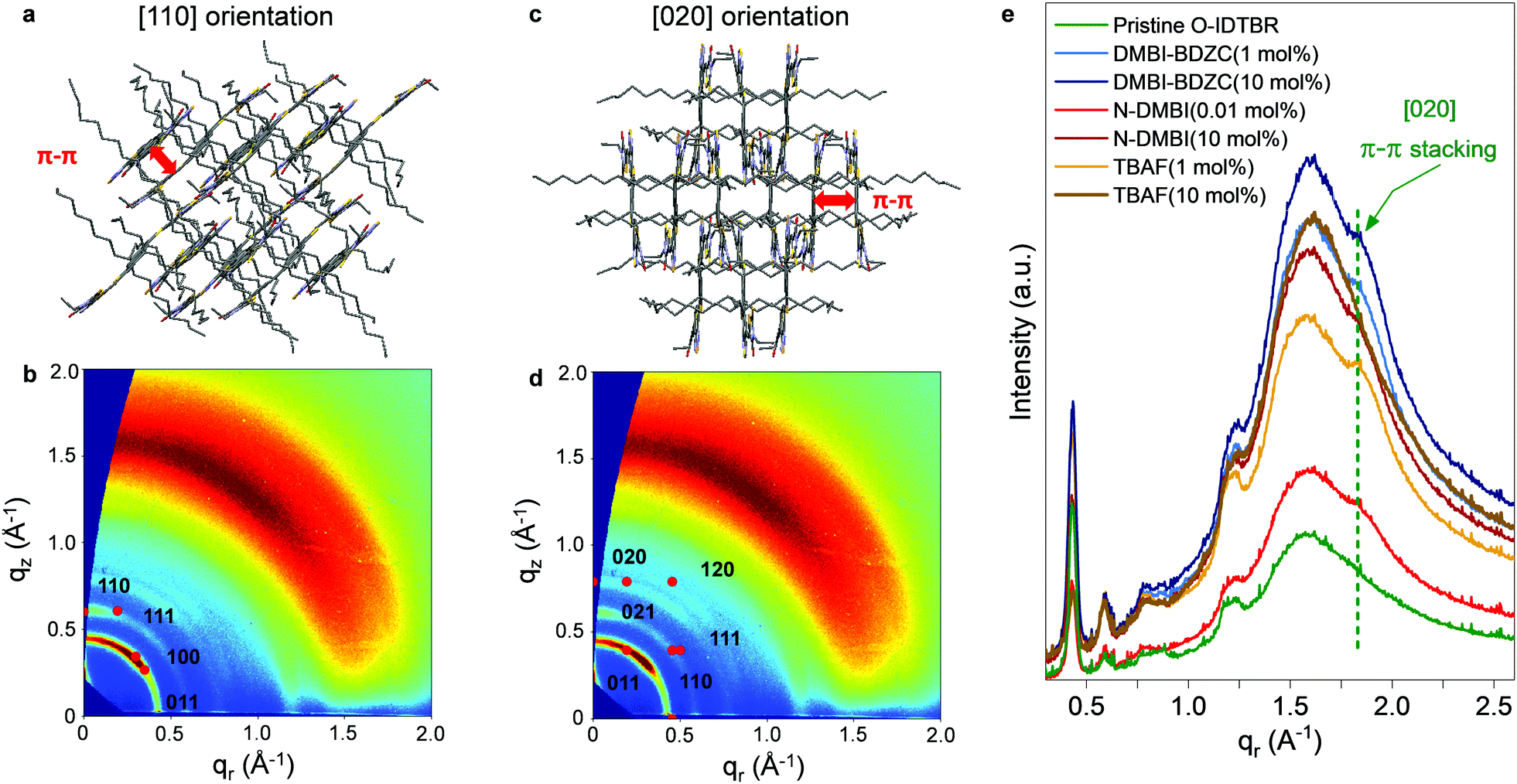 | ||
| Fig. 3 Representative [110] and [020] indexing shown for the mixed-orientation 0.01 mol% N-DMBI thin-film, which produced the best-performing OTFTs overall, including [110] orientation with tilted π–π stacking (a) schematic and (b) indexing and [020] orientation with in-plane π–π stacking (c) schematic and (d) indexing. (e) Integrated plots of GIWAXS patterns along the qr direction (in-plane) for pristine and n-doped films. The latter shows in-plane π-stacking only occurs with the mixed [110] and [020] orientations. | ||
Further evidence of this trend comes from the fact that the fraction of [020] appears to correlates with OTFT μ. To quantify the relative intensity of the two orientations, we calculated the fraction of each orientation across the entire film, from the intensity of the corresponding peaks in qz-direction.39 The results are shown in Fig. S6 and Table S2 (ESI†). We find that, for example, 0.01% N-DMBI contains more [020] than 10 mol% N-DMBI which corresponds to a higher μ. We note here that the fact TBAF(10 mol%) does not exhibit the [020] orientation is unexpected, especially considering its presence in TBAF (1 mol%). This is likely because, at 10 mol%, the system is overloaded beyond the optimum doping concentration, which removes beneficial effects on crystallisation and growth. We also note that the ratio between [110] and [020] appears to be dependent on the type and/or amount of dopant; however, it is difficult to give a quantitative ratio between the two orientations. One experimental approach to investigate these effects further is to study sequential doping via solvent annealing or through sublimation, to first form the thin-film, and then doping to investigate the development of the [020] orientation, when provides with enough thermal energy. However, such focused investigations are beyond the scope of this work.
Theory
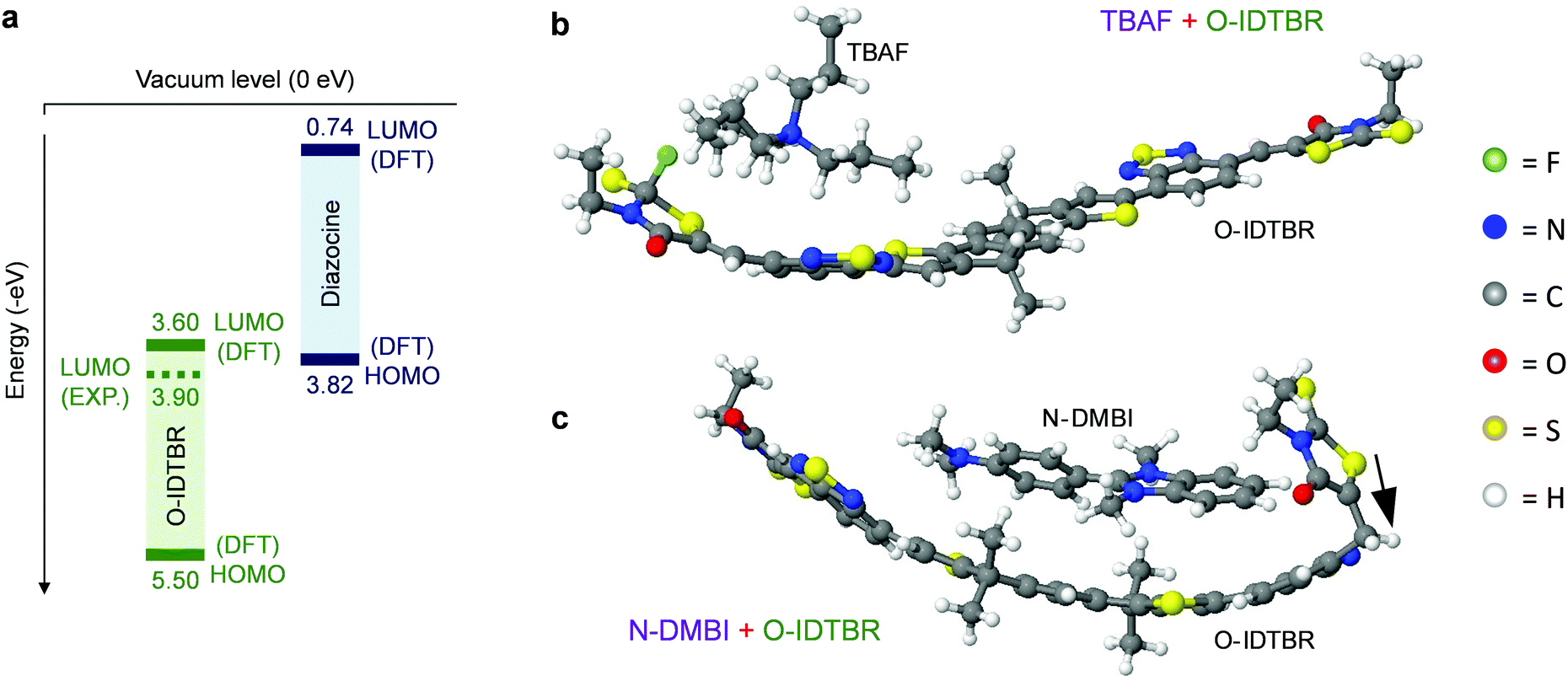 | ||
| Fig. 4 (a) Energy level diagram for integer charge transfer doping of O-IDTBR by DMBI-BDZC. (b) TBAF complex with an O-IDTBR molecule in a configuration where the F-atom is chemisorbed onto a C-atom in the O-IDTBR. (c) N-DMBI complex with an O-IDTBR molecule in a configuration where the H-atom has been transferred from N-DMBI to O-IDTBR, as shown with the black arrow. | ||
One particular question raised by these results is: how can DMBI-BDZC, TBAF and N-DMBI n-dope O-IDTBR via different mechanisms, yet result in the same new structural orientation? For DMBI-BDZC and N-DMBI, the fact that they are from the same family may result in a specific interaction between their functional unit and the O-IDTBR. Although this is extremely difficult to explore with atomic-level DFT calculations, we investigated possible configurations for N-DMBI- and DMBI-BDZC-doped O-IDTBR. We find that, in the case of N-DMBI-doped O-IDTBR, i.e. an O-IDTBR molecule with an H− anion attached (Fig. S7, ESI†), there are a number of possible configurations with comparable energies. This leads to the possibility of various effects on crystal morphology and orientation. For DMBI-BDZC, i.e. a diazocine complex with an O-IDTBR molecule (Fig. S8, ESI†), the O-IDTBR molecule retains a more or less flat configuration, akin to those found for certain structures with N-DMBI (Fig. S7, ESI†). This shows that, although doping mechanisms are different with N-DMBI and DMBI-BDZC, the ensuing structure for the O-ITDBR (or a number of possible such structures) can be similar in the different cases. We find that this is the same for TBAF, i.e. an O-IDTBR molecule with an F− anion attached (Fig. S9, ESI†) in terms of possible configurations with comparable energies. Overall if different O-IDTBR end configurations have comparable energies, the presence DMBI-BDZC, N-DMBI or TBAF could therefore have similar effects on O-IDTBR in terms of crystal morphology and orientation. The final structure depends on the complex details of dopant–host interactions, including complex steric constraints, which are not fully taken into account in small-scale DFT calculations. The similar effects that different dopants can have on morphology is part of a broader, important message from this work, which is the first to highlight such dopant-induced structure–property relationship.
The results outlined in this work suggest that different n-dopants – that rely on different doping mechanisms – lead to similar morphological changes. This raises a poignant question on the origin of the morphology changes and the exact role of the dopant. Possible reasons include, but are not limited to: (i) changes in the packing motif of the host OSC5,6 upon interaction with the dopant during layer deposition; (ii) interactions between neutral and charged molecules while in solution; (iii) space-filling effects;46 and (iv) charge-transfer processes.47 Overall, further understanding of this complex topic and mechanisms governing molecular doping of OSCs, would certainly require further focused research.
![[small mu, Greek, circumflex]](https://www.rsc.org/images/entities/b_char_e0b3.gif) , is highly anisotropic (circa 1:1:10), with the largest component found along the z-axis for both [110] and [020] (Fig. 5b). The latter favors charge transport along the substrate/channel plane. The [020] crystal orientation corresponds to π–π stacking along the substrate, whilst [110] is tilted by ≈45° with respect to the substrate. To account for these differences, was averaged in the substrate plane (see ESI†), leading to calculated values μe = 0.22 cm2 V−1 s−1 and = 0.29 cm2 V−1 s−1 for [110] and [020], respectively. Although μ is ≈25% greater in [020], the similarity suggests the experimentally measured μ values are more likely due to more uniform molecular alignment in the OTFT channel (due to the anisotropic mobility tensor), or from dopant-induced, less defective domain boundaries, and hence shallower trap states in the density of states. The latter can result directly from either doping mechanisms, or morphology enhancements. Interestingly, we also find that μh is similar to μe, with μh = 0.06 cm2 V−1 s−1 and = 0.08 cm2 V−1 s−1 for [110] and [020], respectively. This finding suggests reasonably balanced, intrinsic ambipolar transport in O-IDTBR, in line with its relatively large electron affinity and relatively small ionization energy.50,51 In this study, such ambipolar transport is not observed since the OTFTs are engineered to operate as n-channel devices. Specifically, we have used silver source/drain electrodes coated with a polyethyleneimine (PEIE) injection layer which raises their work function making them ideal for selective electron injection in the LUMO. However, these theoretical results highlight the possibility of p-type doping as a route to enhance μh to match the high μe reported here. Such high ambipolar mobility would be useful for the implementation of complementary logic circuits comprising a single OSC (albeit spatially doped) as the active layer, and will be the subject of further studies.
, is highly anisotropic (circa 1:1:10), with the largest component found along the z-axis for both [110] and [020] (Fig. 5b). The latter favors charge transport along the substrate/channel plane. The [020] crystal orientation corresponds to π–π stacking along the substrate, whilst [110] is tilted by ≈45° with respect to the substrate. To account for these differences, was averaged in the substrate plane (see ESI†), leading to calculated values μe = 0.22 cm2 V−1 s−1 and = 0.29 cm2 V−1 s−1 for [110] and [020], respectively. Although μ is ≈25% greater in [020], the similarity suggests the experimentally measured μ values are more likely due to more uniform molecular alignment in the OTFT channel (due to the anisotropic mobility tensor), or from dopant-induced, less defective domain boundaries, and hence shallower trap states in the density of states. The latter can result directly from either doping mechanisms, or morphology enhancements. Interestingly, we also find that μh is similar to μe, with μh = 0.06 cm2 V−1 s−1 and = 0.08 cm2 V−1 s−1 for [110] and [020], respectively. This finding suggests reasonably balanced, intrinsic ambipolar transport in O-IDTBR, in line with its relatively large electron affinity and relatively small ionization energy.50,51 In this study, such ambipolar transport is not observed since the OTFTs are engineered to operate as n-channel devices. Specifically, we have used silver source/drain electrodes coated with a polyethyleneimine (PEIE) injection layer which raises their work function making them ideal for selective electron injection in the LUMO. However, these theoretical results highlight the possibility of p-type doping as a route to enhance μh to match the high μe reported here. Such high ambipolar mobility would be useful for the implementation of complementary logic circuits comprising a single OSC (albeit spatially doped) as the active layer, and will be the subject of further studies.
 | ||
Fig. 5 (a) Packing of O-IDTBR (side chains are omitted) with spheres showing the geometrical centers of molecules. Lines show charge hopping directions, with electronic couplings J2 ∼ 2J1. Mobility tensor ![[small mu, Greek, circumflex]](https://www.rsc.org/images/entities/b_i_char_e0b3.gif) is visualized by an ellipsoid and is very anisotropic due to orientation of the preferential orientation of long molecular axes along the z-direction. (b) The [110] and [020] orientations of the unit cell with respect to the substrate. is visualized by an ellipsoid and is very anisotropic due to orientation of the preferential orientation of long molecular axes along the z-direction. (b) The [110] and [020] orientations of the unit cell with respect to the substrate. | ||
Experimental
Organic semiconductor preparation
The dopant solutions, as well as the stock O-IDTBR solution, were prepared in chlorobenzene. Doping concentrations were calculated as molar percentages (mol%) of the total O-IDTBR molar mass. The dopant solutions were admixed with the O-IDTBR solution for the various doping concentrations, such that the overall dopant:O-IDTBR solution concentration is always 10 mg mL−1. All dopant:O-IDTBR solutions were stirred overnight at 50 °C prior to the transistor fabrication.Thin-film transistor fabrication and measurements
Top-gate, bottom-contact devices were fabricated on 18 × 18 mm glass substrates cleaned using acetone and IPA, before 15 minutes of UV–ozone treatment. The clean substrates were transferred into an N2-glove box for the remaining transistor fabrication and measurements. 30 nm Ag source-drain contacts were deposited via thermal evaporation through a shadow mask. An initial layer of PEIE (0.04% polyethleneimine in methoxyethanol) was spin-coated at 5000 rpm for 60 s and thermally annealed at 70 °C for 5 minutes. The dopant:O-IDTBR solutions were then spin-coated from warm (70 °C) solutions at 1000 rpm for 30 s, and thermally annealed at 120 °C for 5 minutes, after which the hot-plate was switched off, allowing the devices to gradually cool to room temperature (≈23 °C). A CYTOP dielectric later was then spin-coated at 2000 rpm for 60 seconds to produce a 900 nm thick film, which was annealed at 50 °C for 80 minutes. Finally, a 40 nm Al gate electrode was thermally evaporated through a shadow mask. A Keysight B2912A Precision Source/Measure Unit was used to measure the transistor current–voltage characteristics.Electron paramagnetic resonance
A continuous wave Bruker EMX PLUS spectrometer was used to record the EPR spectra at low temperatures (5 K) using a liquid helium setup, as well as a standard resonator for high sensitivity. The spectra were recorded using 0.625 mW of microwave power with 5 G modulation amplitude and 100 kHz modulation frequency. We have chosen to investigate samples in the solution state, instead of the solid state, for practical purposes related to the accurate positioning of the material in the EPR tube.Atomic force microscopy
Atomic force microscopy (AFM) images were acquired using an Agilent 5500 in tapping mode. Gwyddion was used for image analysis and processing.Grazing-incident wide-angle X-ray scattering
GIWAXS was data was gathered using the 11-BM Complex Materials Scattering (CMS) beamline of the National Synchrotron Light Source II (NSLS-II), Brookhaven National Laboratory. The semiconductor layers were prepared following the same processing steps used for the fabrication of field-effect transistors. The samples were then illuminated using X-rays with a wavelength of 0.0918 nm, at an incident angle of 0.10°. An in-vacuum CCD (Photonic Science) detector – calibrated by silver behenate and located 227 mm away from the thin-film samples – was tilted at ≈19° from the incident X-ray beam direction. To minimize the air scattering, measurements were performed under vacuum at an exposure time of 100 seconds. To gain a better resolution in q-space and limit the X-ray footprint on the sample, the thin films were partially removed to maintain only ∼5 mm length along the X-ray direction. The data analysis was performed by a custom-made program, SciAnalysis, including integrated plots along Qr and Qz directions, as well as the overall patterns.Density functional theory (DFT) calculations
The code NWCHEM52 and B3LYP53,54 exchange–correlation functional were used to perform DFT calculations. The 6-31G* or 6-311G* Gaussian basis sets were typically used to perform structure relaxation. van der Waals interactions were included with the DFT-D3 method.55 The reported DFT HOMO and LUMO energy values utilized the more complete 6-311+G* basis.Computer simulations of charge transport in crystalline O-IDTBR
The initial cell parameters and atomic positions were taken by analysing the X-ray scattering patterns and equilibrated in the NPT ensemble, before evaluating the electronic coupling elements,56 reorganization and site energies.57 The corresponding master equation, with one molecule representing one hopping site, and Markus charge transfer rates were solved using the kinetic Monte Carlo (MC) algorithm. The hole and electron mobilities were evaluated directly from the MC trajectories. All simulations were performed using the GROMACS58,59 and VOTCA-CTP packages,49 where further details are provided in the ESI.†Conclusions
In summary, we employed several different molecular n-type dopants, namely DMBI-BDZC, TBAF and N-DMBI, in transistors made from the prototypical small-molecule O-IDTBR. Under optimal n-doping, we found that all dopant molecules enhanced electron mobility to greater than 1 cm2 V−1 s−1. Analysis of the organic semiconductor using EPR and field-effect measurements show that n-type doping plays a role in the observed electron transport and the measured mobility improvements. Morphology and microstructure analysis by AFM and GIWAXS techniques, on the other hand, revealed that the dopant molecules also behave as morphology-modifiers, and lead to a new, dopant-induced O-IDTBR structural orientation, namely [020]. Theoretical calculations support the idea that the synergistic effects of n-type doping and minute microstructure alterations, are responsible for the improved electron transport, whilst highlighting O-IDTBR as an intrinsically ambipolar material with balanced hole and electron mobilities. By reporting record high NFA mobilities from the simple admixing of molecular dopants and O-IDTBR, we identify beneficial interactions between the dopant and host that result in a dopant-induced packing orientation underpinning previously unreported mechanisms. We investigate this, for the first time, by combining the GIWAXS analysis, single crystal microstructure and molecular modelling to provide a theoretical understanding of the origin of improved electron transport and mobility. Overall, this work demonstrates n-type doping as a powerful technique for improving charge carrier transport in solution-processed n-type small-molecules: the finding that electron transport improves via the coexistence of trap filling and morphology-changes, both establishes and probes a bigger picture relevant to a broad range of organic semiconducting devices – from transistors to photovoltaics,60 – for the development of high-performance organic electronics.Conflicts of interest
There are no conflicts to declare.Acknowledgements
The authors acknowledge the King Abdullah University of Science and Technology (KAUST) for financial support. LT acknowledges the use of the GRNET HPC facility ARIS under project STEM-2. This research used CMS beamline of the National Synchrotron Light Source II, a U.S. Department of Energy (DOE) Office of Science User Facility operated for the DOE Office of Science by Brookhaven National Laboratory under Contract No. DE-SC0012704. DA received funding from the BMBF grants InterPhase and MESOMERIE (FKZ 13N13661, FKZ 13N13656) and the European Union Horizon 2020 research and innovation program ‘‘Widening materials models’’ under Grant Agreement No. 646259 (MOSTOPHOS). D. A. also acknowledges KAUST for hosting his sabbatical. A. M. acknowledges postdoctoral support of the Alexander von Humboldt Foundation.Notes and references
- B. Lussem, M. Riede and K. Leo, Doping of organic semiconductors, 2013 Search PubMed.
- I. E. Jacobs and A. J. Moulé, Adv. Mater., 2017, 29, 1703063 CrossRef PubMed.
- Y. Xu, H. Sun, A. Liu, H.-H. Zhu, W. Li, Y.-F. Lin and Y.-Y. Noh, Adv. Mater., 2018, 30, 1801830 CrossRef PubMed.
- M. Waldrip, O. D. Jurchescu, D. J. Gundlach and E. G. Bittle, Adv. Funct. Mater., 2020, 30, 1904576 CrossRef CAS.
- A. F. Paterson, Y.-H. Lin, A. D. Mottram, Z. Fei, M. R. Niazi, A. R. Kirmani, A. Amassian, O. Solomeshch, N. Tessler, M. Heeney and T. D. Anthopoulos, Adv. Electron. Mater., 2017, 4, 1700464 CrossRef.
- B. Lüssem, C.-M. Keum, D. Kasemann, B. Naab, Z. Bao and K. Leo, Chem. Rev., 2016, 116, 13714–13751 CrossRef PubMed.
- I. Salzmann, G. Heimel, M. Oehzelt, S. Winkler and N. Koch, Acc. Chem. Res., 2016, 49, 370–378 CrossRef CAS PubMed.
- H. Mendez, G. Heimel, A. Opitz, K. Sauer, P. Barkowski, M. Oehzelt, J. Soeda, T. Okamoto, J. Takeya, J.-B. Arlin, J.-Y. Balandier, Y. Geerts, N. Koch and I. Salzmann, Angew. Chem., Int. Ed., 2013, 52, 7751–7755 CrossRef CAS PubMed.
- B. Lüssem, M. Riede and K. Leo, Phys. Status Solidi A, 2013, 210, 9–43 CrossRef.
- A. F. Paterson, L. Tsetseris, R. Li, A. Basu, H. Faber, A.-H. Emwas, J. Panidi, Z. Fei, M. R. Niazi, D. H. Anjum, M. Heeney and T. D. Anthopoulos, Adv. Mater., 2019, 31, 1900871 CrossRef PubMed.
- J. Panidi, A. F. Paterson, D. Khim, Z. Fei, Y. Han, L. Tsetseris, G. Vourlias, P. A. Patsalas, M. Heeney and T. D. Anthopoulos, Adv. Sci., 2018, 5, 1700290 CrossRef PubMed.
- Y. Han, Z. Fei, Y.-H. Lin, J. Martin, F. Tuna, T. D. Anthopoulos and M. Heeney, npj Flexible Electron., 2018, 2, 11 CrossRef.
- J. Panidi, J. Kainth, A. F. Paterson, S. Wang, L. Tsetseris, A.-H. Emwas, M. A. McLachlan, M. Heeney and T. D. Anthopoulos, Adv. Funct. Mater., 2019, 29, 1902784 CrossRef.
- P. Wei, J. H. Oh, G. Dong and Z. Bao, J. Am. Chem. Soc., 2010, 132, 8852–8853 CrossRef CAS PubMed.
- J. Yuan, Y. Zhang, L. Zhou, G. Zhang, H.-L. Yip, T.-K. Lau, X. Lu, C. Zhu, H. Peng, P. A. Johnson, M. Leclerc, Y. Cao, J. Ulanski, Y. Li and Y. Zou, Joule, 2019, 3, 908–909 CrossRef.
- A. Wadsworth, M. Moser, A. Marks, M. S. Little, N. Gasparini, C. J. Brabec, D. Baran and I. McCulloch, Chem. Soc. Rev., 2019, 48, 1596–1625 RSC.
- H. Bristow, K. J. Thorley, A. J. P. White, A. Wadsworth, M. Babics, Z. Hamid, W. Zhang, A. F. Paterson, J. Kosco, J. Panidi, T. D. Anthopoulos and I. McCulloch, Adv. Electron. Mater., 2019, 5, 1900344 CrossRef CAS.
- A. F. Paterson, S. Singh, K. J. Fallon, T. Hodsden, Y. Han, B. C. Schroeder, H. Bronstein, M. Heeney, I. McCulloch and T. D. Anthopoulos, Adv. Mater., 2018, 30, 1801079 CrossRef PubMed.
- J. Kim, D. Khim, K.-J. Baeg, W.-T. Park, S.-H. Lee, M. Kang, Y.-Y. Noh and D.-Y. Kim, Adv. Funct. Mater., 2016, 26, 7886–7894 CrossRef CAS.
- X. Zhao, D. Madan, Y. Cheng, J. Zhou, H. Li, S. M. Thon, A. E. Bragg, M. E. DeCoster, P. E. Hopkins and H. E. Katz, Adv. Mater., 2017, 29, 1606928 CrossRef PubMed.
- S. P. Schießl, H. Faber, Y.-H. Lin, S. Rossbauer, Q. Wang, K. Zhao, A. Amassian, J. Zaumseil and T. D. Anthopoulos, Adv. Mater., 2016, 28, 3952–3959 CrossRef PubMed.
- S. Rossbauer, C. Muller and T. D. Anthopoulos, Adv. Funct. Mater., 2014, 24, 7116–7124 CAS.
- C. W. Koh, J. H. Heo, M. A. Uddin, Y. W. Kwon, D. H. Choi, S. H. Im and H. Y. Woo, ACS Appl. Mater. Interfaces, 2017, 9, 43846–43854 CrossRef CAS PubMed.
- J. Luo, J. Xia, H. Yang, L. Chen, Z. Wan, F. Han, H. A. Malik, X. Zhu and C. Jia, Energy Environ. Sci., 2018, 11, 2035–2045 RSC.
- D. Kiefer, A. Giovannitti, H. Sun, T. Biskup, A. Hofmann, M. Koopmans, C. Cendra, S. Weber, L. J. Anton Koster, E. Olsson, J. Rivnay, S. Fabiano, I. McCulloch and C. Müller, ACS Energy Lett., 2018, 3, 278–285 CrossRef CAS PubMed.
- A. Salleo, Organic Electronics, Wiley-VCH Verlag GmbH & Co. KGaA, 2013, pp. 341–380 DOI:10.1002/9783527650965.ch14.
- H. H. Choi, K. Cho, C. D. Frisbie, H. Sirringhaus and V. Podzorov, Nat. Mater., 2018, 17, 2–7 CrossRef CAS PubMed.
- J. H. Kim, S. W. Yun, B.-K. An, Y. D. Han, S.-J. Yoon, J. Joo and S. Y. Park, Adv. Mater., 2013, 25, 719–724 CrossRef CAS PubMed.
- A. Salleo, Mater. Today, 2007, 10, 38–45 CrossRef CAS.
- C. Liu, G. Li, R. Di Pietro, J. Huang, Y.-Y. Noh, X. Liu and T. Minari, Phys. Rev. Appl., 2017, 8, 034020 CrossRef.
- S. M. Sze, Physics of Semiconductor Devices, John Wiley & Sons, Wiley Eastern Limited, New Delhi, India, 1981 Search PubMed.
- W. L. Kalb and B. Batlogg, Phys. Rev. B: Condens. Matter Mater. Phys., 2010, 81, 035327 CrossRef.
- A. F. Paterson, A. D. Mottram, H. Faber, M. R. Niazi, Z. Fei, M. Heeney and T. D. Anthopoulos, Adv. Electron. Mater., 2019, 5, 1800723 CrossRef.
- N. Gasparini, M. Salvador, T. Heumueller, M. Richter, A. Classen, S. Shrestha, G. J. Matt, S. Holliday, S. Strohm, H.-J. Egelhaaf, A. Wadsworth, D. Baran, I. McCulloch and C. J. Brabec, Adv. Energy Mater., 2017, 7, 1701561 CrossRef.
- C. G. Shuttle, N. D. Treat, J. D. Douglas, J. M. J. Fréchet and M. L. Chabinyc, Adv. Energy Mater., 2012, 2, 111–119 CrossRef CAS.
- Y. Han, C. Jianya, Z. Ke, T. Yabing, M. Xiangyi, X. Xianbin and M. Wei, Adv. Energy Mater., 2018, 0, 1703672 Search PubMed.
- K. V. Nguyen, M. M. Payne, J. E. Anthony, J. H. Lee, E. Song, B. Kang, K. Cho and W. H. Lee, Sci. Rep., 2016, 6, 33224 CrossRef CAS PubMed.
- S. Holliday, R. S. Ashraf, A. Wadsworth, D. Baran, S. A. Yousaf, C. B. Nielsen, C.-H. Tan, S. D. Dimitrov, Z. Shang, N. Gasparini, M. Alamoudi, F. Laquai, C. J. Brabec, A. Salleo, J. R. Durrant and I. McCulloch, Nat. Commun., 2016, 7, 11585 CrossRef CAS PubMed.
- J. W. Ward, R. Li, A. Obaid, M. M. Payne, D.-M. Smilgies, J. E. Anthony, A. Amassian and O. D. Jurchescu, Adv. Funct. Mater., 2014, 24, 5052–5058 CrossRef CAS.
- D. Baran, T. Kirchartz, S. Wheeler, S. Dimitrov, M. Abdelsamie, J. Gorman, R. S. Ashraf, S. Holliday, A. Wadsworth, N. Gasparini, P. Kaienburg, H. Yan, A. Amassian, C. J. Brabec, J. R. Durrant and I. McCulloch, Energy Environ. Sci., 2016, 9, 3783–3793 RSC.
- H. Cha, J. Wu, A. Wadsworth, J. Nagitta, S. Limbu, S. Pont, Z. Li, J. Searle, M. F. Wyatt, D. Baran, J.-S. Kim, I. McCulloch and J. R. Durrant, Adv. Mater., 2017, 29, 1701156 CrossRef PubMed.
- D. Baran, R. S. Ashraf, D. A. Hanifi, M. Abdelsamie, N. Gasparini, J. A. Röhr, S. Holliday, A. Wadsworth, S. Lockett, M. Neophytou, C. J. M. Emmott, J. Nelson, C. J. Brabec, A. Amassian, A. Salleo, T. Kirchartz, J. R. Durrant and I. McCulloch, Nat. Mater., 2017, 16, 363–369 CrossRef CAS PubMed.
- R.-Z. Liang, M. Babics, V. Savikhin, W. Zhang, V. M. Le Corre, S. Lopatin, Z. Kan, Y. Firdaus, S. Liu, I. McCulloch, M. F. Toney and P. M. Beaujuge, Adv. Energy Mater., 2018, 8, 1800264 CrossRef.
- B. D. Naab, S. Guo, S. Olthof, E. G. B. Evans, P. Wei, G. L. Millhauser, A. Kahn, S. Barlow, S. R. Marder and Z. Bao, J. Am. Chem. Soc., 2013, 135, 15018–15025 CrossRef CAS PubMed.
- I. Denti, S. Cimò, L. Brambilla, A. Milani, C. Bertarelli, M. Tommasini and C. Castiglioni, Chem. Mater., 2019, 31, 6726–6739 CrossRef CAS.
- R. Yu, H. Yao, Z. Chen, J. Xin, L. Hong, Y. Xu, Y. Zu, W. Ma and J. Hou, Adv. Mater., 2019, 31, 1900477 CrossRef PubMed.
- P. Y. Yee, D. T. Scholes, B. J. Schwartz and S. H. Tolbert, J. Phys. Chem. Lett., 2019, 10, 4929–4934 CrossRef CAS PubMed.
- C. Poelking and D. Andrienko, J. Chem. Theory Comput., 2016, 12, 4516–4523 CrossRef CAS PubMed.
- V. Rühle, A. Lukyanov, F. May, M. Schrader, T. Vehoff, J. Kirkpatrick, B. Baumeier and D. Andrienko, J. Chem. Theory Comput., 2011, 7, 3335–3345 CrossRef PubMed.
- N. B. Kotadiya, A. Mondal, P. W. M. Blom, D. Andrienko and G.-J. A. H. Wetzelaer, Nat. Mater., 2019, 18, 1182–1186 CrossRef CAS PubMed.
- D. Abbaszadeh, A. Kunz, N. B. Kotadiya, A. Mondal, D. Andrienko, J. J. Michels, G.-J. A. H. Wetzelaer and P. W. M. Blom, Chem. Mater., 2019, 31, 6380–6386 CrossRef CAS.
- M. Valiev, E. J. Bylaska, N. Govind, K. Kowalski, T. P. Straatsma, H. J. J. V. Dam, D. Wang, J. Nieplocha, E. Aprá, T. L. Windus and W. A. de Jong, Comput. Phys. Commun., 2010, 181, 1477–1489 CrossRef CAS.
- A. D. Becke, J. Chem. Phys., 1993, 98, 5648–5652 CrossRef CAS.
- P. J. Stephens, F. J. Devlin, C. F. Chabalowski and M. J. Frisch, J. Phys. Chem., 1994, 98, 11623–11627 CrossRef CAS.
- S. Grimme, J. Antony, S. Ehrlich and H. Krieg, J. Chem. Phys., 2010, 132, 154104 CrossRef PubMed.
- B. Baumeier, J. Kirkpatrick and D. Andrienko, Phys. Chem. Chem. Phys., 2010, 12, 11103–11113 RSC.
- C. Poelking, E. Cho, A. Malafeev, V. Ivanov, K. Kremer, C. Risko, J.-L. Brédas and D. Andrienko, J. Phys. Chem. C, 2013, 117, 1633–1640 CrossRef CAS.
- B. Hess, C. Kutzner, D. van der Spoel and E. Lindahl, J. Chem. Theory Comput., 2008, 4, 435–447 CrossRef CAS PubMed.
- B. Hess, D. van der Spoel, E. Lindahl, J. C. Smith, M. R. Shirts, P. Bjelkmar, P. Larsson, P. M. Kasson, R. Schulz, R. Apostolov, S. Pronk and S. Páll, Bioinformatics, 2013, 29, 845–854 CrossRef PubMed.
- Y. Lin, Y. Firdaus, M. I. Nugraha, F. Liu, S. Karuthedath, A.-H. Emwas, W. Zhang, A. Seitkhan, M. Neophytou, H. Faber, E. Yengel, I. McCulloch, L. Tsetseris, F. Laquai and T. D. Anthopoulos, Adv. Sci., 2020, 7, 1903419 CrossRef CAS PubMed.
Footnote |
| † Electronic supplementary information (ESI) available. See DOI: 10.1039/d0tc05861k |
| This journal is © The Royal Society of Chemistry 2021 |