
 Open Access Article
 This Open Access Article is licensed under a Creative Commons Attribution-Non Commercial 3.0 Unported Licence
Charge transport in phthalocyanine thin-film transistors coupled with Fabry–Perot cavities†
Evan S. H.
Kang
 *ab,
Shangzhi
Chen
a,
Vedran
Đerek‡
a,
Carl
Hägglund
c,
Eric D.
Głowacki
a and
Magnus P.
Jonsson
*a
*ab,
Shangzhi
Chen
a,
Vedran
Đerek‡
a,
Carl
Hägglund
c,
Eric D.
Głowacki
a and
Magnus P.
Jonsson
*a
aLaboratory of Organic Electronics, Department of Science and Technology (ITN), Linköping University, 60174, Norrköping, Sweden. E-mail: magnus.jonsson@liu.se; eshkang@chungbuk.ac.kr
bDepartment of Physics, Chungbuk National University, Cheongju 28644, Republic of Korea
cDivision of Solar Cell Technology, Department of Materials Science and Engineering, Uppsala University, P.O. Box 35, 75103 Uppsala, Sweden
First published on 15th January 2021
Abstract
Strong light-matter coupling can form hybrid states at new energy levels that share properties of both light and matter. This principle offers new routes to control material functions without modifying the chemical structure of molecules. In this work, we coupled ambipolar semiconducting thin films to a Fabry–Perot cavity and investigated effects on charge transport. By constructing thin-film transistors inside optical cavities, we could simultaneously study coupling features and charge transport in the same samples. The cavity resonance was detuned by controlling the thickness of the top spacer layer in the cavity. We found no significant influence on charge transport for our systems, which may be related to insufficiently strong coupling. Possible additional origins and future directions are also discussed.
Introduction
Placing molecules in confined optical fields in terms of both space and energy can alter the energy levels of the molecules via strong coupling between molecular resonances and optical resonances.1–6 The new hybrid polariton states show part-light and part-matter nature, accompanied by the possibility for intriguing phenomena such as low-threshold polariton lasing,7,8 high harmonic generation9,10 and Bose–Einstein condensation.11,12 Strong coupling has also been reported to directly affect the material properties of molecular systems, including chemical reactivity,13–17 long-range energy transfer,18–21 and work functions.22 Furthermore, ultrafast microscopy studies demonstrated long-range exciton-polariton transport over several microns for an organic material strongly coupled to a Fabry–Perot cavity.23 This cavity-enhanced exciton transport was supported by theoretical studies.24,25 Theoretical reports also proposed that the formation of hybrid polariton states can affect charge transport, either by opening an additional transport channel contributing to electrical current,26 or by delocalizing not only the polaritonic states but also the electronic states in the conduction27 and valence bands,28 thereby overcoming limitations due to molecular disorder. Excitingly, such coupling-induced enhancements of charge transport were experimentally reported in both n-type27 and p-type28 organic semiconductors strongly coupled to plasmonic nanohole arrays. For other systems, researchers did not observe conductivity enhancement upon strong coupling, including for ambipolar semiconducting polymers coupled with a plasmonic surface lattice resonance29 and carbon nanotubes,30 p-type31 or ambipolar32 polymers coupled with cavity resonances. Thus, the conditions required for coupling processes to affect charge transport remain elusive.In this paper, we investigate charge transport in ambipolar organic thin-film transistors coupled to a Fabry–Perot cavity (Fig. 1). The ambipolar characteristics enabled investigation of both electron and hole transport. Furthermore, the device configuration allowed for both optical and electrical measurements on the same system before (coupling off) and after completing the cavity (coupling on). Completing the cavity led to the formation of three-fold polariton states originating from coupling between two exciton resonances and one cavity resonance. We found only negligible changes in electron and hole transport upon coupling the ambipolar transistors to the optical cavity. We discuss possible explanations to the findings based on Hopfield coefficient analysis and anticrossing in experimental and simulated data.
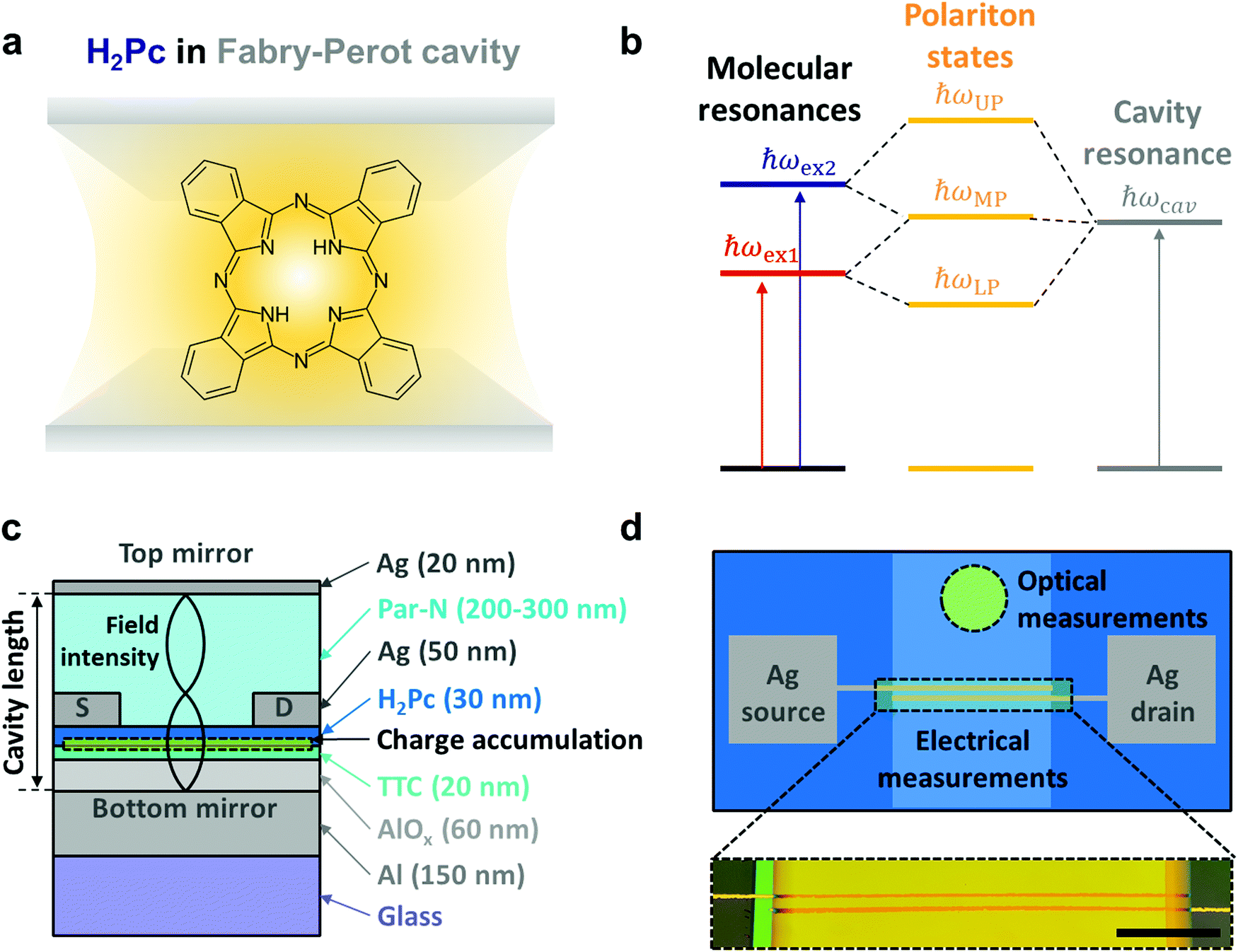 | ||
| Fig. 1 (a) Molecular structure of H2Pc in Fabry–Perot cavity. (b) Coupling scheme between the molecules with two exciton resonances and a cavity. (c) Transistor-in-cavity device configuration. (d) Top view of the same device with optical and electrical measurement areas indicated. The enlarged bottom image of the electrical measurement area was obtained using an optical microscope. The scale bar equals 500 μm. | ||
Results and discussion
Metal-free phthalocyanine (H2Pc) was utilized in this study as a balanced ambipolar semiconducting molecule with decent oscillator strength (Fig. 1a).33,34 Since H2Pc has two exciton resonances (ħωex1 for the lower energy exciton and ħωex2 for the higher energy exciton), we expect three-fold exciton-polariton branches (ħωUP for the upper polariton, ħωMP for the middle polariton and ħωLP for the lower polariton) when strongly coupled with a cavity resonance (ħωcav) (Fig. 1b). Transistor-in-cavity structures were constructed as illustrated in Fig. 1c. The aluminum layer at the bottom acts both as the bottom gate electrode of the transistor and as the bottom mirror of the Fabry–Perot cavity. An electrochemically-grown aluminum oxide (Al2O3) layer35 and a thermally-evaporated tetratetracontane (TTC) layer were used as transistor gate insulator (with capacitance of approx. 60 nF cm−2) and as a bottom spacer layer of the optical cavity. The TTC layer also helps to passivate electron traps on the oxide surface, which is essential for the ambipolarity.36 On top of these layers, we applied H2Pc as the active layer, followed by definition of silver source and drain electrodes. To complete the optical cavity, we used parylene–N (Par–N) as a top spacer layer and a silver layer as top mirror. We tuned the cavity length (i.e. the optical path length between the bottom and top mirrors) and corresponding cavity resonance via the thickness of the Par–N layer (see Fig. S1 in ESI† for thickness optimization). Fig. 1d illustrates a top view of the final multi-layered structure. Optical and electrical measurement areas were close to each other on the same sample, and the optical microscopy image of the electrical measurement area reveals uniform layers with well-defined layer edges (Fig. 1d).We determined the optical absorption (A) of the samples via A = 1 − R, where R is the reflection of the sample when illuminated from the top by normal incident light. The absorption spectra of H2Pc inside a cavity with 240 nm of Par–N clearly shows three peaks corresponding to the three-fold polariton states (ħωUP, ħωMP, ħωLP) (Fig. 2a). These peaks are differently positioned compared to the original exciton resonances (ħωex1 ∼ 1.76 and ħωex2 ∼ 1.95 eV), as shown in the extinction spectrum of H2Pc without cavity coupling. The cavity resonance could be detuned by changing the Par–N thickness, as shown in Fig. 2b. We used the 2nd order cavity resonance throughout this work to enable detuning without concern of electrical leakage, as would have been an issue for the 1st order resonance due to too thin top spacer layers. For 270 nm of Par–N (red solid line), both the 2nd and 3rd order cavity mode resonances (the leftmost and rightmost peaks, respectively) are located far from ħωex1 and ħωex2 (indicated by vertical dashed lines), leaving the exciton peaks almost unaffected from their non-coupled positions. As the Par–N thickness decreases, both cavity resonances blue-shift to higher energies. When the 2nd order resonance enters the region of the exciton resonances, three absorption peaks appear at energies that do not overlap with the original exciton resonances. This result indicates the formation of three-fold polariton states. The experimentally observed spectral features, including the exciton and cavity resonances and their coupling, were successfully reproduced by finite-difference time-domain (FDTD) simulations (Fig. 2c). Fig. 2d presents anticrossing plots obtained by extracting the peak positions from Fig. 2b and 2c. The x-axis represents the non-coupled 2nd order cavity resonance, as determined using the positions of the non-coupled 3rd order resonance for each thickness (see Fig. S2 in ESI†). The results clearly show anticrossing behaviour and gradual formation of three polariton branches as the cavity resonance is tuned to the exciton resonances.
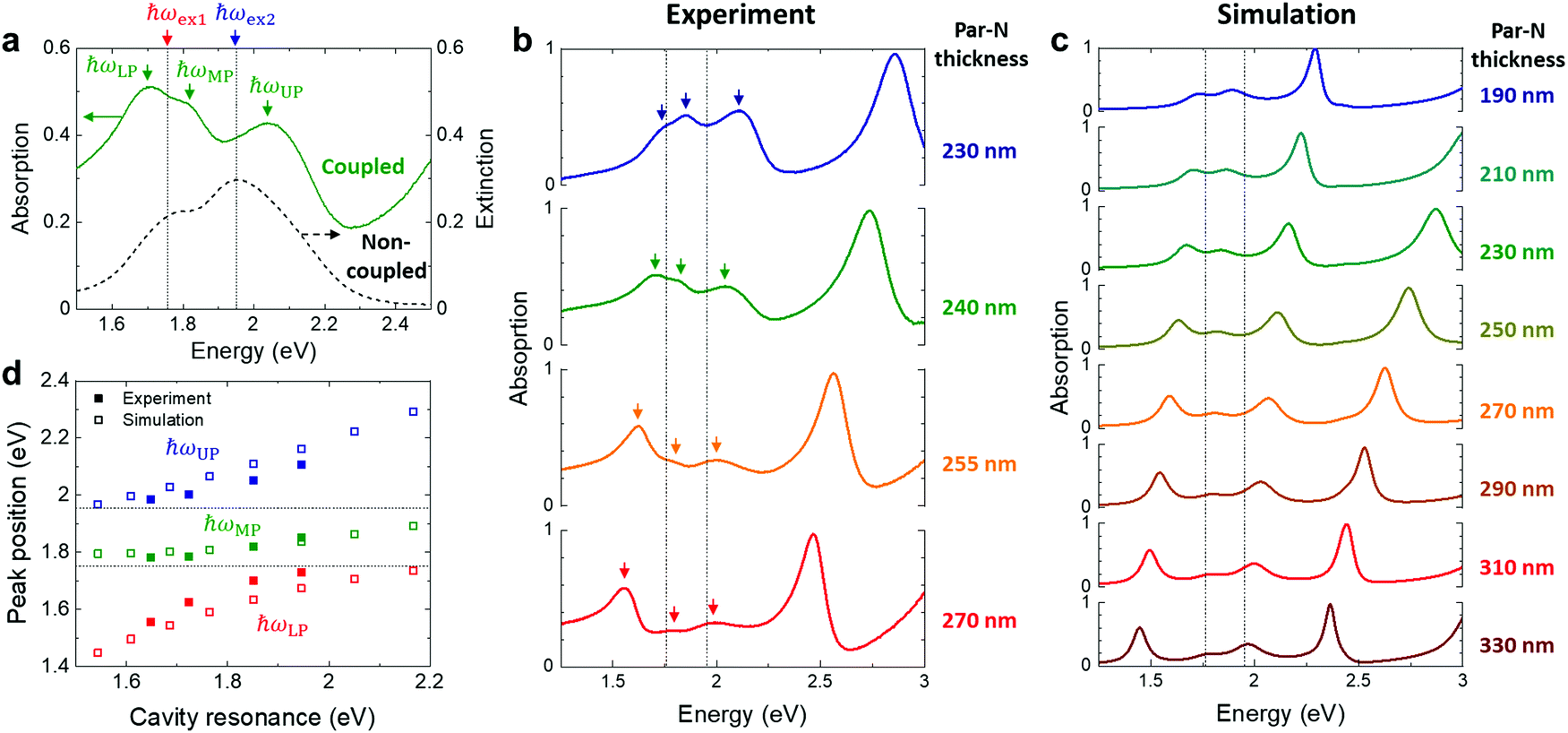 | ||
| Fig. 2 (a) Absorption spectrum for a device with H2Pc in a cavity with Par–N thickness of 240 nm and extinction spectrum for the H2Pc without cavity coupling. (b) Measured and (c) simulated absorption spectra for devices with H2Pc in cavities of different Par–N thicknesses. (d) Anticrossing plot constructed using the peak positions in (b) and (c). | ||
To study possible effects of coupling on charge transport, we performed electrical measurements on transistors on the same samples as investigated optically above. We carried out two sets of measurements for each device: one before deposition of the top silver mirror (i.e. ‘without top mirror’) and one after deposition of the top mirror (i.e. ‘with top mirror’). This allowed us to determine the characteristics of the same transistors with and without cavity coupling. Fig. 3 presents the transfer curves in p-type (left column) and n-type (middle column) operation modes. For p-type operation, we used a drain–source voltage (Vds) of −10 V while Vds was set to 10 V for n-type operation. The gate-source current (Igs) could be maintained at least one order of magnitude lower than the drain–source current (Ids) during the whole measurements. Together with decent Ids on–off ratio (∼104 for p-type and ∼103 for n-type operation), this indicates robust transistor operations. Regardless of Par–N thickness and corresponding cavity resonance, we found no significant differences in transfer characteristics before (dashed lines) and after (solid lines) adding the cavity top mirrors.
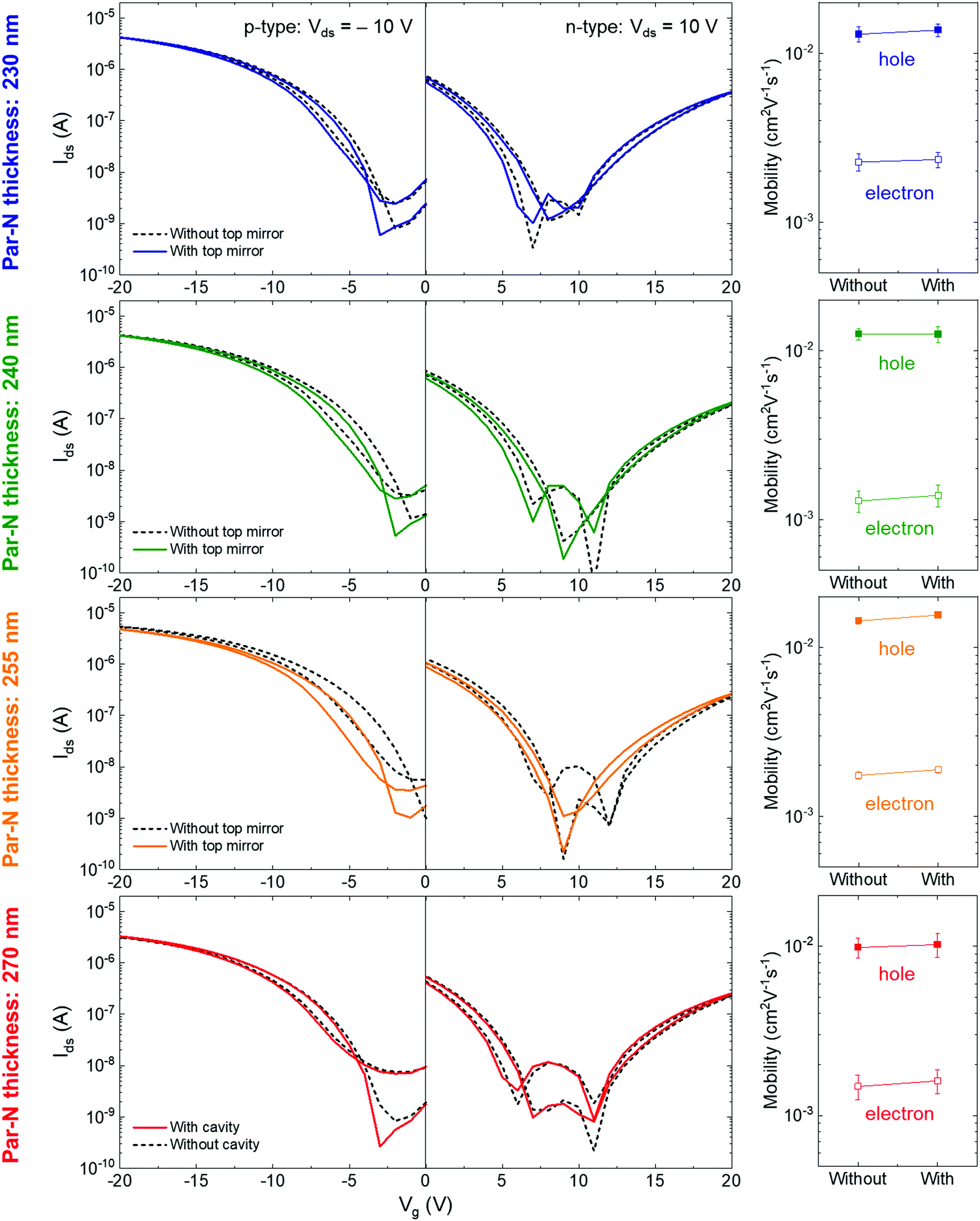 | ||
| Fig. 3 Transfer curves in p-type and n-type operation modes for the transistors with and without top mirror (left panel). The different rows correspond to different Par-N thicknesses, as indicated in the figure. Hole and electron mobility values extracted from the transfer curves (right panels). Error bars represent the standard deviation of the mobility values for multiple devices. | ||
We calculated the charge carrier mobilities from the transfer curves, assuming that the transistors work in the linear regime. As shown in the right column of Fig. 3, neither electron nor hole mobility showed noticeable enhancements or reductions after the completion of the cavities. The plots indicate a small mobility increase for the completed cavities in many cases, but these changes fall within the standard deviation when averaging over 3–5 devices on each sample.
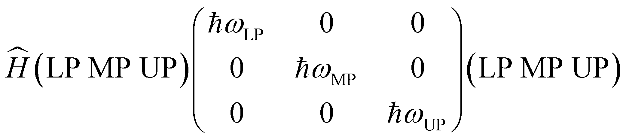
The fact that adding the top mirrors did not clearly affect the transistors’ charge transport performance may be related to different factors, including the details of the coupling process between the cavity and the molecules. In order to investigate the coupling strength and to understand how each polariton branch is constituted, we employ the Hamiltonian of the coupled system,3,37,38
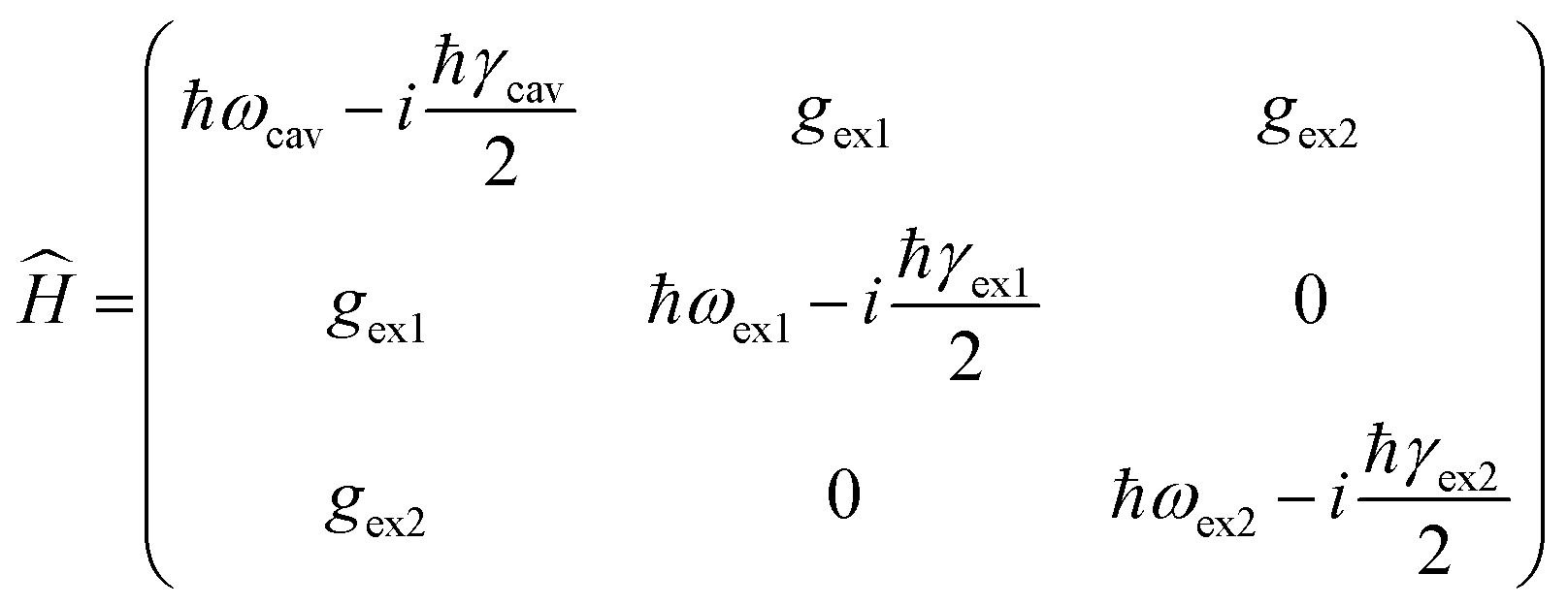 | (1) |
 | (2) |
| ħΩ UP–LP (meV) | ħΩ UP–MP (meV) | ħΩ MP–LP (meV) | ħγ cav (meV) | ħγ ex1 (meV) | ħγ ex2 (meV) | g ex1 (meV) | g ex2 (meV) | |
|---|---|---|---|---|---|---|---|---|
| Exp | 360 | 238 | 122 | 152 | 213 | 380 | 76 | 146 |
| Sim | 454 | 272 | 182 | 105 | 264 | 276 | 122 | 174 |
The Hopfield coefficients represent how each polariton branch is intermixed between the original cavity and the two exciton contributions. They are plotted as a function of cavity resonance in Fig. 4b and d for the three polariton branches. For both experiments (Fig. 4b) and simulations (Fig. 4d), all polariton branches have nonzero contributions from all three original resonances. Furthermore, the middle polariton branch, particularly in the experiments, possesses fairly balanced intermixing approaching 33% fraction of each original resonance near zero detuning. The formation of intermixed polariton states opens up the possibility that the electronic structure of the molecules may be modified from the non-coupled molecules. On the other hand, the electrical measurements suggest that the coupling did not affect the factors that determines the charge transport in our transistors. One reason for obtaining the same electrical transport properties with and without the top mirrors could be that the coupling between the molecules and the cavity is not sufficiently strong. To identify a system as being in the strong coupling regime, it is common to require the coupling-induced splitting to be larger than the widths of the original resonance peaks. Based on the values presented in Table 1, the splitting between the outermost polariton branches ħΩUP–LP seemingly satisfies this criteria. However, for a three-fold polariton system, the energy difference between the upper and lower polaritons will never be smaller than the difference between the original exciton resonances (190 meV for our system). Hence, ħΩUP–LP may not on its own be sufficient to judge in which coupling regime the system is. If we instead investigate the splittings that involve the middle polariton branch, we note that the strong coupling criteria (ħΩ > (ħγcav + ħγex1,ex2)/2) are not always satisfied. For example, ħΩMP–LP is slightly smaller than (ħγcav + ħγex1)/2 or (ħγcav + ħγex2)/2 for the simulated results, and considerably smaller for the experimental results. This implies that the system may be only near the border to the strong coupling regime. It is possible that the requirements for the coupling to influence transport properties include stronger coupling strengths for our type of systems.
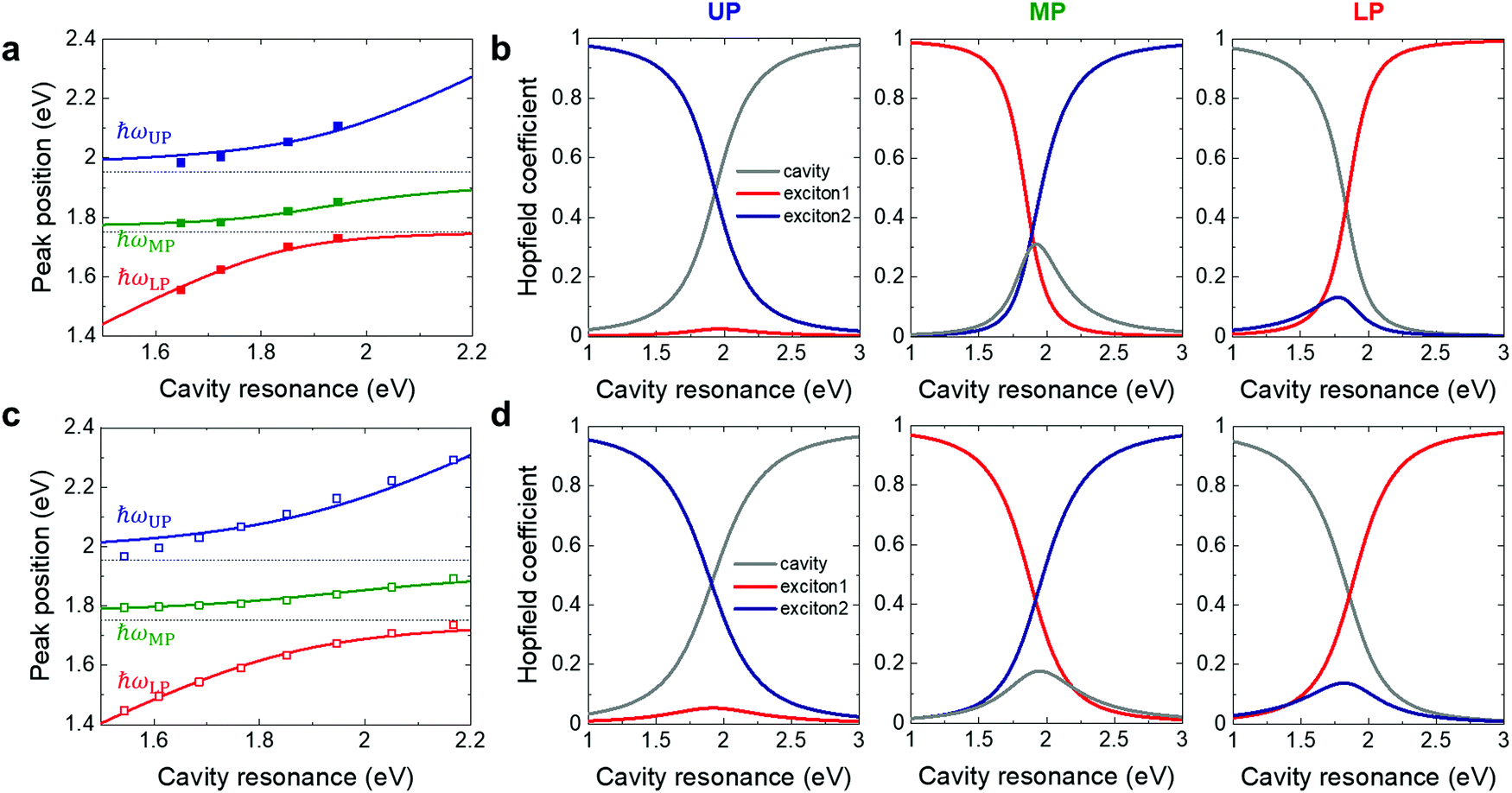 | ||
| Fig. 4 (a) Numerical curve fits using eqn (1) and (2) to the experimental data. (b) Hopfield coefficients for cavity and exciton contributions to UP (left panels), MP (middle panels), and LP (right panels) states as a function of cavity resonance. (c and d) Results corresponding to (a and b) for simulated data. | ||
Enhancement in electrical conductivity was observed upon strong coupling to plasmonic nanohole arrays but to our knowledge not (yet) to Fabry–Perot cavities. We note in that respect that normal incident Fabry–Perot modes have zero in-plane momentum whereas plasmonic nanohole modes provide non-zero in-plane momentum. This intrinsic difference between the two types of cavities could influence their ability to affect charge transport upon strong coupling. On the other hand, the choice of normal incidence for the optical investigation of the Fabry–Perot cavities was experimentally convenient but the electrical measurements are made in the dark without any well-defined angle. Hence, it is relevant to discuss polaritonic states coupled to Fabry–Perot modes also at other angles than normal incidence, which have non-zero in-plane momentum. Simulations at different incident angles for cavities with the same resonances as in the experiments illustrate the dispersive nature of the polariton branches and show clear anticrossing features (Fig. 5, see Fig. S4 (ESI†) for the raw spectra). In agreement with the Hopfield analysis above, zero detuning for normal incidence occurs for thickness between 230 nm (corresponding resonance ∼1.95 eV) and 250 nm (corresponding resonance ∼1.85 eV). As the thickness of Par-N increases, the cavities become detuned at normal incidence and instead achieve zero detuning at larger incidence angles, which can be identified from the minimum splitting between the upper and lower polariton branches (the vertical black lines in the lower panels of Fig. 5). The angle at zero detuning increases to around 55° for the thickest cavity (300 nm), albeit with smaller minimum splitting and coupling strength compared with those of the thinner cavities. These results imply that polariton states with non-zero in-plane momenta are present in the cavities, and for thicker Par–N they also correspond to zero detuning. Considering that our charge transport measurements showed no effect for either thin or thick samples (Fig. 3), we can therefore not attribute the lack of enhanced charge transport to the lack of modes with in-plane momenta.
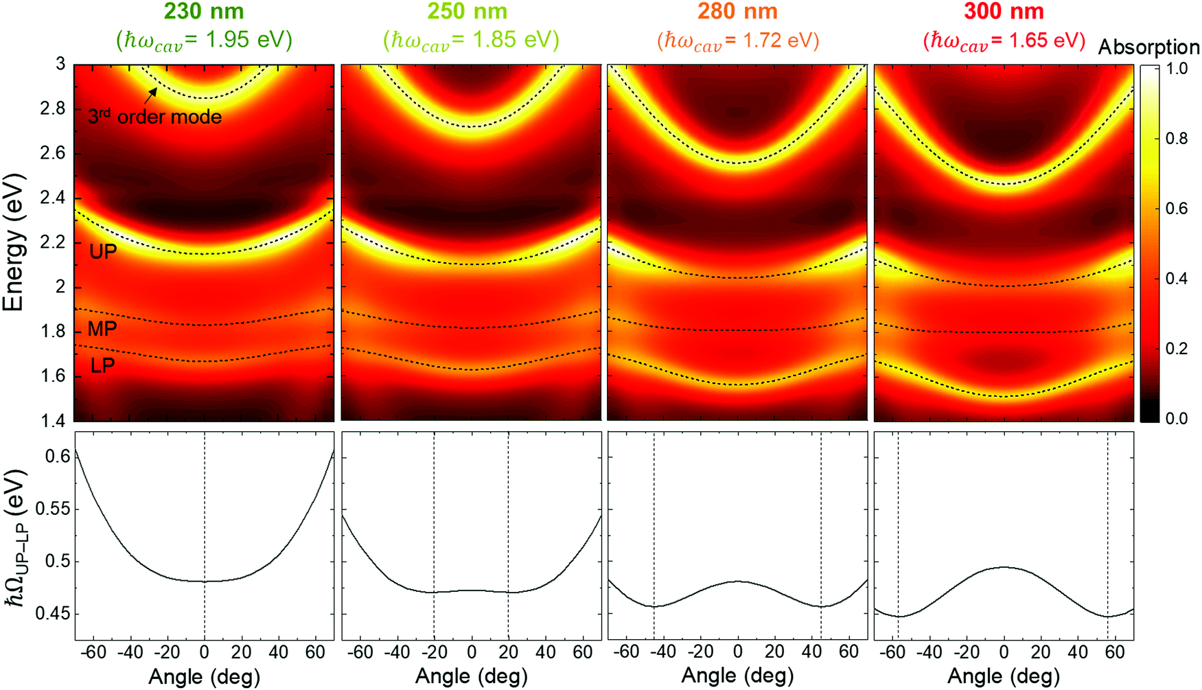 | ||
| Fig. 5 Angle-resolved absorption spectra using FDTD simulation for different thicknesses of Par–N (and corresponding cavity resonances). The black dashed lines in upper panels indicate 3rd order cavity mode, UP, MP and LP peak positions from top to bottom. as a function of angle is displayed in lower panels. The angles associated with the minimum splitting are designated with the vertical black dashed lines. | ||
It should also be pointed out that the observed splitting stems from the coupling with the whole ensemble of molecules inside the cavity while the electrical transport characteristics originate from the accumulation region at the semiconductor-gate insulator interface of the transistors, where the charge transport takes place (see Fig. 1c). Because of non-uniform optical field distribution across the cavity, there is a risk that the molecules in the transistor responsible for charge transport are not strongly coupled at zero detuning even when the total cavity shows sufficiently large splitting values. In this respect, it is important to find the “Goldilocks zone” where the molecules at the interface are strongly coupled, by optimizing the position of the transistor accumulation region within the cavity and sweeping the cavity length. Furthermore, although thicker layers can provide larger splittings (scaling with the square root of the number of molecules involved in the coupling process),39 we intentionally kept the H2Pc layer relatively thin (∼30 nm) to maintain fairly uniform optical field across this layer. Even thinner layers would result in yet smaller splittings and less strong coupling, as confirmed by FDTD simulations (see Fig. S5 and Table S1 in ESI†). All things considered, it is still not beyond doubt that the molecules at the interface for our system are truly in the strong coupling regime. Future work may avoid such ambiguity using ultrathin layers of molecules with larger oscillator strengths.
The intrinsic (non-coupled) electrical transport properties may also influence the likelihood of enhancing transport properties upon strong coupling. For our system, the electron and hole mobilities are on the order of 10−3 cm2 V−1 s−1 and 10−2 cm2 V−1 s−1, respectively. These values are relatively high and it may be easier to obtain clear enhancements for systems with lower intrinsic mobilities.40 Additionally, considering the polycrystalline nature of phthalocyanine thin films,36 we cannot rule out possible local enhancement effects within grains yet that are not observable due to transport across grain boundaries being the main limiting factor to the measured currents. However, in that respect we note that previous studies reporting enhanced conductivity upon strong coupling also utilized organic semiconductors known to form polycrystalline films, and with similar charge carrier mobilities.27,28 We further note that the exciton-polaritons in our system carry no net charge, because they originate from excitons consisting of one negatively charged electron and one positively charged hole. Future work may investigate charge transport also for polaritons composed of quasiparticles with nonzero net charge, such as polaron-polaritons41,42 or trion-polaritons,38,43 which can readily drift under applied external electric fields.
Conclusions
In summary, we report optical coupling between ambipolar semiconducting organic molecules and a Fabry–Perot cavity, and study its direct effect on charge transport using transistor-in-cavity structures. Although the strong coupling criteria were not clearly satisfied, the formation of hybrid polariton states with moderate splitting and anticrossing indicates that the system is at least near the border of strong coupling. Furthermore, Hopfield coefficients demonstrated that the intermixed polariton states are composed of balanced contributions from all three original resonances. Charge transport studies showed no clear effects of coupling on the electron and hole charge carrier mobilities, and we discussed possible reasons for these results.Conflicts of interest
There are no conflicts of interest to declare.Acknowledgements
The authors acknowledge funding from the Wenner–Gren Foundations, the Swedish Research Council (including Reg. No. 621-2014-5599), the Swedish Foundation for Strategic Research, the ÅForsk foundation, National Research Foundation of Korea (NRF) grant funded by the Korea government (MSIT) (No. 2020R1A2C1102558) and Swedish Government Strategic Research Area in Materials Science on Functional Materials at Linköping University (Faculty Grant SFO-Mat-LiU o 2009 00971).References
- D. Sanvitto and S. Kéna-Cohen, Nat. Mater., 2016, 15, 1061 CrossRef CAS.
- D. S. Dovzhenko, S. V. Ryabchuk, Y. P. Rakovich and I. R. Nabiev, Nanoscale, 2018, 10, 3589 RSC.
- D. G. Baranov, M. Wersäll, J. Cuadra, T. J. Antosiewicz and T. Shegai, ACS Photonics, 2018, 5, 24 CrossRef CAS.
- M. Hertzog, M. Wang, J. Mony and K. Börjesson, Chem. Soc. Rev., 2019, 48, 937 RSC.
- E. S. H. Kang, M. Shiran Chaharsoughi, S. Rossi and M. P. Jonsson, J. Appl. Phys., 2019, 126, 140901 CrossRef.
- F. Herrera and J. Owrutsky, J. Chem. Phys., 2020, 152, 100902 CrossRef CAS.
- M. Ramezani, A. Halpin, A. I. Fernández-Domínguez, J. Feist, S. R.-K. Rodriguez, F. J. Garcia-Vidal and J. G. Rivas, Optica, 2017, 4, 31 CrossRef CAS.
- J. W. Kang, B. Song, W. Liu, S. J. Park, R. Agarwal and C. H. Cho, Sci. Adv., 2019, 5, eaau9338 CrossRef CAS.
- T. Chervy, J. Xu, Y. Duan, C. Wang, L. Mager, M. Frerejean, J. A. W. Münninghoff, P. Tinnemans, J. A. Hutchison, C. Genet, A. E. Rowan, T. Rasing and T. W. Ebbesen, Nano Lett., 2016, 16, 7352 CrossRef CAS.
- F. Barachati, J. Simon, Y. A. Getmanenko, S. Barlow, S. R. Marder and S. Kéna-Cohen, ACS Photonics, 2018, 5, 119 CrossRef CAS.
- A. J. Moilanen, T. K. Hakala and P. Törmä, ACS Photonics, 2018, 5, 54 CrossRef CAS.
- J. Keeling and S. Kéna-Cohen, Annu. Rev. Phys. Chem., 2020, 71, 435 CrossRef CAS.
- T. Schwartz, J. A. Hutchison, C. Genet and T. W. Ebbesen, Phys. Rev. Lett., 2011, 106, 196405 CrossRef CAS.
- J. A. Hutchison, T. Schwartz, C. Genet, E. Devaux and T. W. Ebbesen, Angew. Chem., Int. Ed., 2012, 51, 1592 CrossRef CAS.
- A. Thomas, J. George, A. Shalabney, M. Dryzhakov, S. J. Varma, J. Moran, T. Chervy, X. Zhong, E. Devaux, C. Genet, J. A. Hutchison and T. W. Ebbesen, Angew. Chem., Int. Ed., 2016, 55, 11462 CrossRef CAS.
- B. Munkhbat, M. Wersäll, D. G. Baranov, T. J. Antosiewicz and T. Shegai, Sci. Adv., 2018, 4, eaas9552 CrossRef.
- A. Thomas, K. Nagarajan, R. M. A. Vergauwe, J. George, T. Chervy, A. Shalabney, E. Devaux, C. Genet, J. Moran and T. W. Ebbesen, Science, 2019, 363, 615 CrossRef CAS.
- D. M. Coles, N. Somaschi, P. Michetti, C. Clark, P. G. Lagoudakis, P. G. Savvidis and D. G. Lidzey, Nat. Mater., 2014, 13, 712 CrossRef CAS.
- X. Zhong, T. Chervy, S. Wang, J. George, A. Thomas, J. A. Hutchison, E. Devaux, C. Genet and T. W. Ebbesen, Angew. Chem., Int. Ed., 2016, 55, 6202 CrossRef CAS.
- X. Zhong, T. Chervy, L. Zhang, A. Thomas, J. George, C. Genet, J. A. Hutchison and T. W. Ebbesen, Angew. Chem., Int. Ed., 2017, 56, 9034 CrossRef CAS.
- M. Du, L. A. Martínez-Martínez, R. F. Ribeiro, Z. Hu, V. M. Menon and J. Yuen-Zhou, Chem. Sci., 2018, 9, 6659 RSC.
- J. A. Hutchison, A. Liscio, T. Schwartz, A. Canaguier-Durand, C. Genet, V. Palermo, P. Samorì and T. W. Ebbesen, Adv. Mater., 2013, 25, 2481 CrossRef CAS.
- G. G. Rozenman, K. Akulov, A. Golombek and T. Schwartz, ACS Photonics, 2018, 5, 105 CrossRef CAS.
- J. Feist and F. J. Garcia-Vidal, Phys. Rev. Lett., 2015, 114, 196402 CrossRef.
- J. Schachenmayer, C. Genes, E. Tignone and G. Pupillo, Phys. Rev. Lett., 2015, 114, 1 CrossRef.
- D. Hagenmüller, J. Schachenmayer, S. Schütz, C. Genes and G. Pupillo, Phys. Rev. Lett., 2017, 119, 223601 CrossRef.
- E. Orgiu, J. George, J. A. Hutchison, E. Devaux, J. F. Dayen, B. Doudin, F. Stellacci, C. Genet, J. Schachenmayer, C. Genes, G. Pupillo, P. Samorì and T. W. Ebbesen, Nat. Mater., 2015, 14, 1123 CrossRef CAS.
- K. Nagarajan, J. George, A. Thomas, E. Devaux, T. Chervy, S. Azzini, K. Joseph, A. Jouaiti, M. W. Hosseini, A. Kumar, C. Genet, N. Bartolo, C. Ciuti and T. W. Ebbesen, ACS Nano, 2020, 14, 10219 CrossRef CAS.
- Y. Zakharko, M. Held, A. Graf, T. Rödlmeier, R. Eckstein, G. Hernandez-Sosa, B. Hähnlein, J. Pezoldt and J. Zaumseil, ACS Photonics, 2016, 3, 2225 CrossRef CAS.
- A. Graf, M. Held, Y. Zakharko, L. Tropf, M. C. Gather and J. Zaumseil, Nat. Mater., 2017, 16, 911 CrossRef CAS.
- J. K. Asane, V. N. Peters, R. Alexander, T. Wallace, D. A. Peters and M. A. Noginov, J. Nanophotonics, 2019, 13, 026007 CAS.
- M. Held, A. Graf, Y. Zakharko, P. Chao, L. Tropf, M. C. Gather and J. Zaumseil, Adv. Opt. Mater., 2018, 6, 1700962 CrossRef.
- M. Kraus, S. Haug, W. Brütting and A. Opitz, Org. Electron., 2011, 12, 731 CrossRef CAS.
- O. A. Melville, B. H. Lessard and T. P. Bender, ACS Appl. Mater. Interfaces, 2015, 7, 13105 CrossRef CAS.
- E. D. Głowacki, M. Irimia-Vladu, M. Kaltenbrunner, J. Gsiorowski, M. S. White, U. Monkowius, G. Romanazzi, G. P. Suranna, P. Mastrorilli, T. Sekitani, S. Bauer, T. Someya, L. Torsi and N. S. Sariciftci, Adv. Mater., 2013, 25, 1563 CrossRef.
- M. Kraus, S. Richler, A. Opitz, W. Brütting, S. Haas, T. Hasegawa, A. Hinderhofer and F. Schreiber, J. Appl. Phys., 2010, 107, 3 CrossRef.
- J. J. Hopfield, Phys. Rev., 1958, 112, 1555 CrossRef CAS.
- J. Cuadra, D. G. Baranov, M. Wersäll, R. Verre, T. J. Antosiewicz and T. Shegai, Nano Lett., 2018, 18, 1777 CrossRef CAS.
- E. S. H. Kang, S. Chen, S. Sardar, D. Tordera, N. Armakavicius, V. Darakchieva, T. Shegai and M. P. Jonsson, ACS Photonics, 2018, 5, 4046 CrossRef CAS.
- A. Salleo, Nat. Mater., 2015, 14, 1 CrossRef.
- C. Y. Cheng, R. Dhanker, C. L. Gray, S. Mukhopadhyay, E. R. Kennehan, J. B. Asbury, A. Sokolov and N. C. Giebink, Phys. Rev. Lett., 2018, 120, 17402 CrossRef CAS.
- N. Krainova, A. J. Grede, D. Tsokkou, N. Banerji and N. C. Giebink, Phys. Rev. Lett., 2020, 124, 177401 CrossRef CAS.
- C. Möhl, A. Graf, F. J. Berger, J. Lüttgens, Y. Zakharko, V. Lumsargis, M. C. Gather and J. Zaumseil, ACS Photonics, 2018, 5, 2074 CrossRef.
Footnotes |
| † Electronic supplementary information (ESI) available. See DOI: 10.1039/d0tc05418f |
| ‡ Current affiliation: Department of Physics, Faculty of Science, University of Zagreb, Bijenička c. 32, 10000 Zagreb, Croatia. |
| This journal is © The Royal Society of Chemistry 2021 |