
 Open Access Article
 This Open Access Article is licensed under a
 Creative Commons Attribution 3.0 Unported Licence
Non-fullerene-based organic photodetectors for infrared communication†
Maxime
Babics
 *a,
Helen
Bristow
b,
Weimin
Zhang
c,
Andrew
Wadsworth
b,
Marios
Neophytou
c,
Nicola
Gasparini
a and
Iain
McCulloch
*bc
*a,
Helen
Bristow
b,
Weimin
Zhang
c,
Andrew
Wadsworth
b,
Marios
Neophytou
c,
Nicola
Gasparini
a and
Iain
McCulloch
*bc
aDepartment of Chemistry and Centre for Plastic Electronics, Imperial College London, London, W12 0BZ, UK
bDepartment of Chemistry, Chemistry Research Laboratory, University of Oxford, Oxford, OX1 3TA, UK. E-mail: iain.mcculloch@chem.ox.ac.uk
cKing Abdullah University of Science and Technology, KAUST Solar Center, Physical Sciences and Engineering Division (PSE), Thuwal, Saudi Arabia
First published on 11th January 2021
Abstract
Solution-processed organic photodetectors (OPDs) sensitive to infrared (IR) light have the potential to be used in various technologies from health monitoring to communication. These detectors require low bandgap materials absorbing photons beyond 750 nm with high responsivity. In this work, an ultra-low bandgap non-fullerene acceptor (NFA) that absorbs light until 1020 nm is developed. Used in a bulk heterojunction (BHJ)-based device, the photodetector has a maximum responsivity of 0.50 A W−1 at 890 nm without bias voltage comparable with silicon-based detectors. Due to high and balanced mobilities of 10−4 cm2 V−1 s−1, the device has a fast speed of response to IR (i.e. rise and decay time less than 4 μs) and minor damping of 1 dB in the IR communication range (38–50 kHz). The organic photodetector transcripts with accuracy the message emitted around 910 nm from a commercial remote control, thus demonstrating the potential of organic electronics for infrared communication.
Introduction
Benefiting from the progress of organic solar cells (OSCs), organic photodetectors (OPDs), devices that convert a light signal into an electrical signal, have shown in parallel rapid improvement.1–3 OPDs have potential be used for a wide range of application such as imaging,4–7 artificial vision,8,9 wearable electronics,10,11 medical monitoring12 or light communication.13 Historically the development of OPDs has largely focused on detection of visible light, however, the research effort has recently moved towards IR light with applications in biomedical monitoring, imaging or communication.11,14,15 Even though IR OPDs were successfully implemented in the ubiquitous photoplethysmogram sensors,14,16 other examples of real-life applications have been very limited.11,17 To demonstrate the potential of organic materials for IR detection, it is essential to incorporate them on other technologies, IR communication being one of them.Two key properties are necessary for materials used for IR communication employed for remote controls. Firstly, the semiconductor needs to absorb the IR region of the electromagnetic spectrum. Since the emission spectrum of a typical commercial gallium arsenide Light Emitting Diode (LED) used for IR communication is centered around 910 nm, materials with ultra-low bandgap (i.e. 1.1–1.3 eV) are required, where ideally the peak of absorption matches the peak of the LED emission. In the early days of IR fullerene-based OPDs, the low band gap material were polymers donors. The first examples of IR photodetector were reported in 2007 where the devices were active up to the wavelengths of 1200 nm.18,19 This was later improved, with the report of a detector responding until 1450 nm.20 Despite years of development, the main limitation of using fullerene-based BHJ is, with a notable exception,21 the low external quantum efficiency (EQE) in the infrared region (typically less than 30% at 900 nm).22–25 Replacing fullerene by non-fullerene acceptors (NFAs) was an important milestone for OSCs.26–28 If ultralow bandgap NFAs were originally developed to extend the absorption of the solar spectrum and thus give more current in a solar cell, they could also be used to specifically target IR radiation. Due to their high extinction coefficient and the ability to form adequate BHJ, OSCs with low bandgap NFAs maintain high EQE in the IR region (more than 60% at 900 nm).29–31 For the same reason, recent OPD works that target IR use low bandgap NFAs.16,32
The second necessary property for IR communication employed for remote controls is a speed of response (SR) adequate for this technology. Difficult to predict precisely, the cutoff frequency (ftr) is usually limited by the transit time of the charge carriers and is given by the following equation:
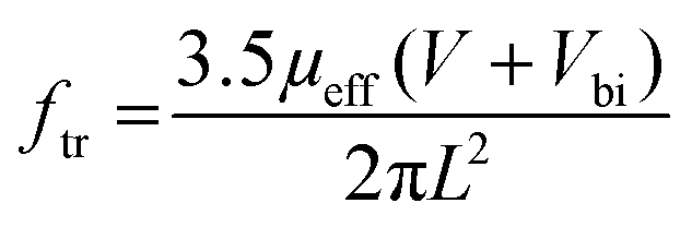 | (1) |
In the equation, μeff is the effective carrier mobility, V is the applied bias, Vbi is the built-in voltage and L is the thickness of the active layer.16,33 Reported values have been of from kHz to MHz3,18,34 where MHz is particularly attractive for visible light communication (VLC).35–37 Since the frequency range used for IR communication by a remote control is between 38 kHz and 50 kHz, the semiconductor with a carrier mobility superior of 10−5 cm2 V−1 s−1 will be necessary for fast extraction of the charges in order to follow the input signal with an attenuation of the response below 3 db.38 To summarize, the ideal candidate for infrared communication is an ultra-low bandgap material with high mobility.
Results and discussions
To fulfil those requirements, we selected and developed a set of two low bandgaps molecules, namely O4TIC and O4TFIC (Scheme 1) with the following strategies. (i) Instead of an indacenodithiophene (IDT) core with bridging methylene units, we opt for the carbon–oxygen-bridged ladder-type bridge which has a stronger electron-donating capability via the conjugation effect of the oxygen.39 (ii) The phenyl moiety in the centre of the molecule is replaced by the electron-rich thieno[3,2-b]thiophene that further improves the electron-donating capability and further reduces the bandgap of the molecule.40 (iii) We attach linear side chains instead of phenyl–alkyl ones to increase the crystallinity and thus increase the electron mobility.41,42 (iv) For the fluorinated version of the molecule, the F atoms enhance the electron-withdrawing capability of the end units thus leading to an even smaller bandgap.43 The lactone 139 was reacted with octylmagnesium bromide to form the four hydroxyl intermediate. This was followed by dehydration to afford dipyran unit 2 in the presence of p-toluene sulfonic acid. Aldehyde 3 was obtained by Vilsmeier–Haack reaction with phosphorus oxychloride and dry dimethylformamide. The target molecules O4TIC and O4TFIC were synthesized by the Knoevenagel condensation reaction of aldehyde 3 with 2-(3-oxo-2,3-dihydro-1H-inden-1-ylidene)malononitrile and 2-(5,6-difluoro-3-oxo-2,3-dihydro-1H-inden-1-ylidene)malononitrile, respectively.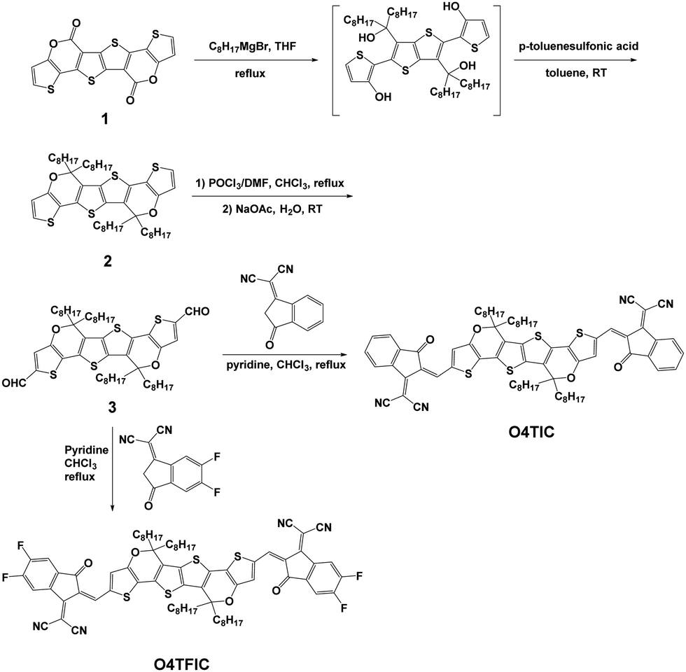 | ||
| Scheme 1 Synthetic route of O4TIC and O4TFIC. | ||
The detailed synthesis protocol is provided in the ESI† and the NFAs are depicted in Fig. 1a alongside PM6, the donor polymer used in this study. PM6 was chosen for its high performance in BHJ devices achieving high mobilities and high responsivity.28,44Fig. 1b shows the thin films UV-vis spectra of the neat materials cast from chlorobenzene (CB) solutions. (UV-vis of blends provided Fig. S1, ESI†). The onset of absorption of O4TIC is around 920 nm and the absorption maximum is at 825 nm. The absorption of O4TFIC, red-shifted as expected from the fluorination, starts around 1020 nm and peaks at 920 nm. The large bandgap donor PM6 has a maximum absorption at 625 nm. From the onset of absorption, the optical bandgaps (Eg) are 1.8, 1.4 and 1.2 eV for PM6, O4TIC and O4TFIC respectively. The emission of a commercial LED, used for IR communication, is superimposed and shows a narrow peak centered around 915 nm. Importantly, the emission of the LED matches with the maximum absorption of O4TFIC whereas there is reduced overlap between O4TIC absorption and the LED emission. Fig. 1c depicts the energy levels of the materials. The Ionization Potential (IP) is measured via Photoelectron spectroscopy (PESA) and the Electron affinity (EA) is obtained by adding the optical band gap to the IP. The IP of PM6 is 5.4 eV and the IP levels of O4TIC and O4TFIC are 5.6 and 5.7 eV respectively (Fig. S2, ESI†). The EA of O4TIC and O4TFIC are 4.2 eV and 4.5 eV respectively. The energy offset between PM6 and the acceptors make them suitable for fabricating OPDs devices based on bulk heterojunctions (BHJ).
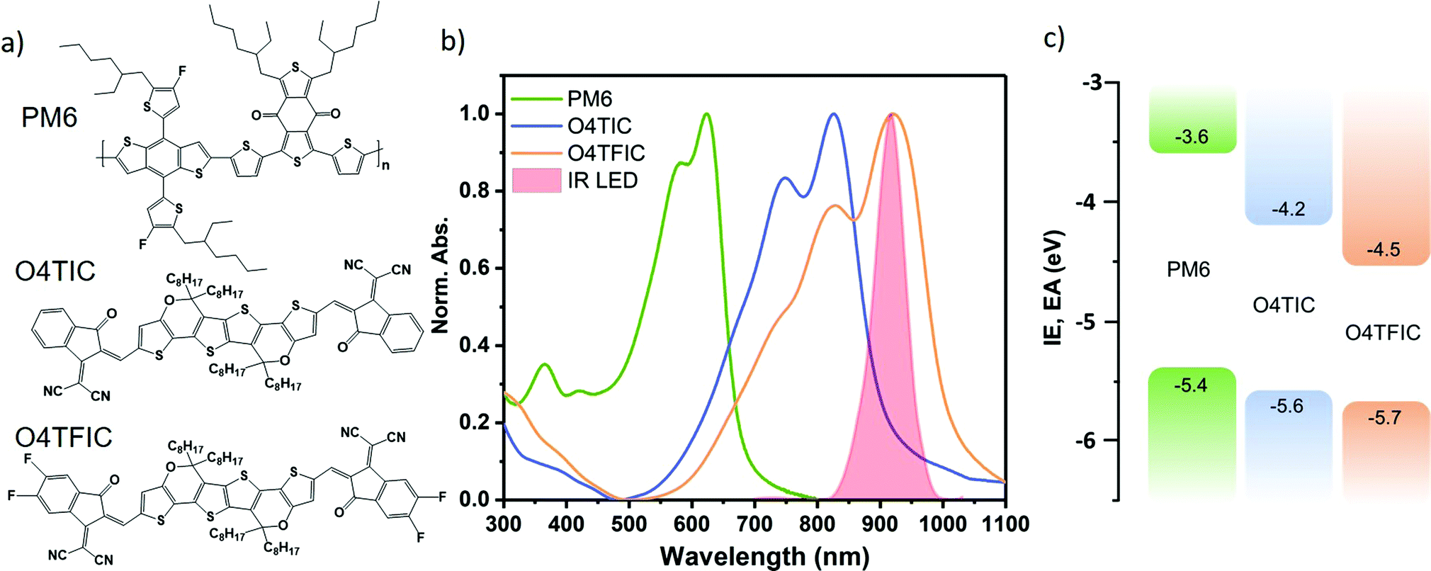 | ||
| Fig. 1 (a) The chemical structures and (b) the thin-film UV-vis absorption spectra of O4TIC, O4TFIC and PM6. The emission spectrum of a LED used for infrared communication is presented. (c) PESA-estimated values of IP and EA. EA values calculated by subtracting IP and Eg values. | ||
Organic photodetectors were fabricated using the device structure ITO/PEDOT:PSS/BHJ/Phen-NaDPO/Ag. The detailed experimental protocol is provided in the SI. To characterize the devices under operation we use an infrared LED emitting at 880 nm (spectrum is given Fig. S3, ESI†). The dark current and the current measured under light are provided in Fig. 2a. At reverse bias (−2 V or 2.2 × 10⁷ V m −1) the photodetectors show comparable dark current values of 74 μA cm−2 and 83 μA cm−2 for PM6:O4TIC and PM6:O4TFIC respectively. The relatively large values of dark current, several orders of magnitude higher than silicon photodiodes, for devices containing low bandgap materials have been explained previously by the injection of electrons into the LUMO of the acceptor and/or device leakage.2 Common ways to reduce the dark current include the interlayers engineering and/or increasing the thickness of the active layer.2,45,46 Our results on device optimization show a decrease of dark current by increasing the thickness of the active layer but in this is accompanied by a reduction in responsivity (Fig. S4 and Table S1, ESI†). Under IR illumination, the devices show an increase of current up to 6.9 mA cm−2 and 15.2 mA cm−2 for PM6:O4TIC and PM6:O4TFIC respectively. The increase of current of several orders of magnitude demonstrates the sensitivity of the detectors to IR light.
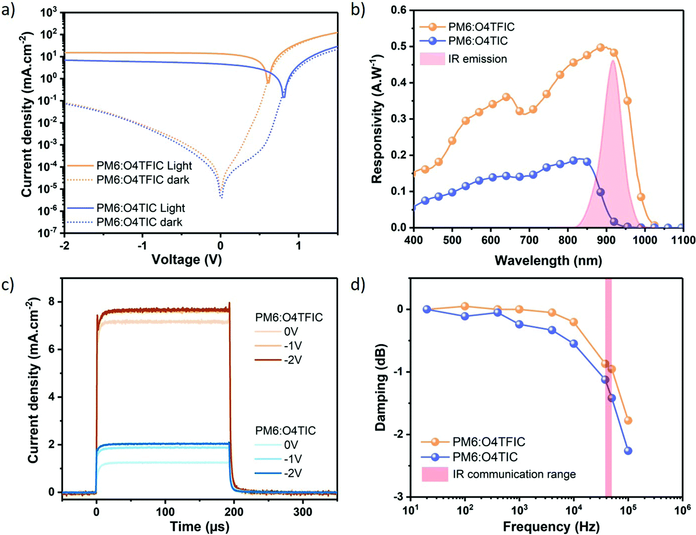 | ||
| Fig. 2 (a) Current–voltage measurement of PM6:O4TIC and PM6:O4TFIC devices in dark and under IR light (b) responsivity of PM6:O4TIC and PM6:O4TFIC devices, the emission of an LED used for infrared communication is plotted (c) transient current of PM6:O4TIC and PM6:O4TFIC devices in response to 200 μs infrared LED pulse for various voltage biases applied (d) normalized photoresponse of PM6:O4TIC and PM6:O4TFIC devices as a function of the modulation frequency of an IR LED at −2 V. The frequency range used for infrared communication (38–50 kHz) is shown in red. A bias of −2 V is equivalent to an electric field of F = 2.2 × 10⁷ V m−1. | ||
The responsivity of the devices is depicted in Fig. 2b. PM6:O4TIC reaches a maximum responsivity of 0.19 A W−1 at 830 nm. For PM6:O4TFIC the responsivity is higher, extending into the infra-red region up to 1020 nm and reaches 0.50 A W−1 at 890 nm without applying voltage bias. At this wavelength, the responsivity is similar to Si-based photodetectors (Fig. S5, ESI†). The higher responsivity of PM6:O4TFIC compared to PM6:O4TIC is in line with the higher current measured under IR light.
An assessment of the sensitivity of organic photodetectors can be made using the parameter specific detectivity (D*) which combines the responsivity and noise current. Estimations of the noise current in the OPDs accounting for contributions of thermal, shot and flicker noise were used to determine the specific detectivities as outlined in the ESI.† For the PM6:O4TFIC OPD at 915 nm an impressive D* of 9 × 10¹¹ Jones is determined at 0 V (Fig. S6, ESI†). However, from the dark current density plot (Fig. 2a) and noise current spectral density plot (Fig. S7, ESI†) it can be seen that at increasing reverse bias the specific detectivity will be limited by noise.
As mentioned above, a suitable material for IR application not only absorbs IR light but also has the requisite speed of response. Infrared communication doesn’t work with continuous light but rather pulsed light at frequencies between 38 kHz to 50 kHz depending on the manufacturer. The reasons are to avoid overheating of the source and prevent absorption of parasitic light by the receiver. Thus, it is necessary to investigate the speed of response of the devices and their behaviour under different light frequencies. Performing transient photocurrent (TPC) measurements, we measure at the rise and decay time (time to go from 10% to 90% of the steady-state response) of the devices following a 200 μs IR light pulse for different applied voltages. The results are provided in Fig. 2c (Normalized data depicted in Fig. S8, ESI†). For the blend PM6:O4TIC without applying bias, the rise time is 8.1 μs and the decay time 9.2 μs. At −2 V the rise time decreases to 3.8 μs and the decay to 4.3 μs. Turning to PM6:O4TFIC device, the rise time is almost independent of the applied bias and slightly decrease from 2.9 to 2.4 μs from unbiased to −2 V. The decay time decreases from 3.9 μs to 3.7 μs. It is well established that devices work faster with applied bias since the velocity of the carriers increases proportionally with the voltage.34,47 The transient time of PM6:O4TFIC implies fast extraction of carriers required for fast operation.
Finally, we investigate the decay of the device response for different frequencies of a sinusoidal IR signal (i.e. damping), with results provided in Fig. 2d. The PM6:O4TIC photodetector response decreases gradually until 10 kHz before a more abrupt decay. The decay observed for infrared communication range is 1.12 dB and 1.41 dB for 38 kHz and 50 kHz respectively. PM6:O4TFIC demonstrates better stability at low frequency with minor damping up to 10 kHz. At 38 kHz and 50 kHz, the damping is only 0.87 dB and 0.95 dB respectively. This corresponds to a decrease in the signal of only around 10% compared to the signal under continuous illumination.
To better understand the origin of the difference in performance between the two blends we evaluated the Space Charge Limited Current (SCLC) mobilities. (details provided in the ESI†). The neat NFAs show relatively comparable electron mobilities of 1.4 and 2.3 × 10⁻⁴ cm2 V−1 s−1 for O4TIC and O4TFIC respectively. Comparing the blends, the hole mobilities are also similar 1.1 and 2.5 × 10⁻⁴ cm2 V−1 s−1 for O4TIC and O4TFIC respectively, and comparable to the neat donor PM6 (1.7 × 10⁻⁴ cm2 V−1 s−1). However, the electron mobility in the PM6:O4TIC blend is significantly reduced to 2.9 × 10⁻⁶ cm2 V−1 s−1 whereas PM6:O4TFIC keeps a similar high mobility of 1.3 × 10⁻⁴ cm2 V−1 s−1. These different blend mobilities explain why PM6:O4TFIC has a better responsivity and faster response than its non-fluorinated counterpart. In summary, PM6:O4TFIC shows large current variation between dark and illuminated, high responsivity to IR light, fast extraction of carriers and good performance at high frequencies, all criteria needed for IR communication.
To demonstrate the potential of organic electronics for IR communication, we tested the PM6:O4TFIC photodetector response to the signal emitted by a commercial IR remote control. The controller here uses the NEC transmission protocol consisting of the Pulse Distance Encoding (PDE) of the message bits where the logical “0” and “1” depends on the time between two pulse bursts.38 The signal emitted from the remote control when the button “On” is engaged is depicted in Fig. 3a. It contains different parts in the following order: a start pulse of 9 ms followed by a 4.5 ms space. The first 8-bit corresponds to the address for the receiving device (i.e. the device ID), here a series of eight “0”. The device ID is followed by its logical inverse: eight “1”. The third 8-bit series corresponds to the command. Here the command “on” of the remote control is the sequence 10![[thin space (1/6-em)]](https://www.rsc.org/images/entities/char_2009.gif) 110000 followed again by its logical inverse. A final pulse burst ends the transmission. The total message is 67.5 ms long. The inset of Fig. 3a shows the sinusoidal nature of the pulse burst at the frequency of 38 kHz. Fig. 3b shows our organic photodetector response to the message. The device captures the signal sequence with a clear distinction between “0” and “1” bits and a high ratio of light on/light off. A current density of mA cm−2 is measured due to the high responsivity of the device in the IR region in agreement with the previous measurement. The inset shows the device response to 38 kHz sinusoidal pulse. This experiment demonstrates that the organic photodetector can be integrated into the mature technology of IR communication.
110000 followed again by its logical inverse. A final pulse burst ends the transmission. The total message is 67.5 ms long. The inset of Fig. 3a shows the sinusoidal nature of the pulse burst at the frequency of 38 kHz. Fig. 3b shows our organic photodetector response to the message. The device captures the signal sequence with a clear distinction between “0” and “1” bits and a high ratio of light on/light off. A current density of mA cm−2 is measured due to the high responsivity of the device in the IR region in agreement with the previous measurement. The inset shows the device response to 38 kHz sinusoidal pulse. This experiment demonstrates that the organic photodetector can be integrated into the mature technology of IR communication.
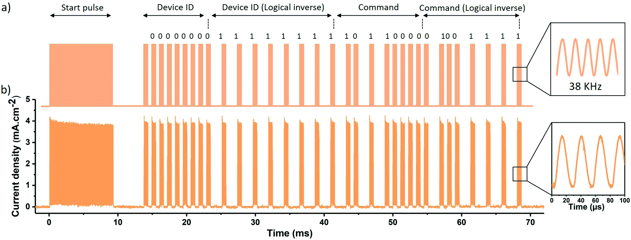 | ||
| Fig. 3 (a) Message frame delivered by the “On” button. The protocol uses a Pulse Distance Encoding of the message bits (b) response of PM6:O4TFIC photodetector to the message frame. | ||
Conclusion
We have developed a low bandgap molecule absorbing light until 1020 nm. Used in a BHJ-based photodetector, the device shows high responsivity in the IR region. Due to high and balanced mobilities, the detector has a fast response to IR light. The photodetector can follow the message emitted from a remote control showing the potential of organic electronics for IR communication.Conflicts of interest
There are no conflicts to declare.Acknowledgements
The research reported in this publication was supported by funding from King Abdullah University of Science and Technology Office of Sponsored Research (OSR) under awards no. OSR-2018-CARF/CCF-3079, no. OSR-2015-CRG4-2572 and OSR -4106 CPF2019. We acknowledge EC FP7 Project SC2 (610115), EC H2020 (643791), and EPSRC Projects EP/G037515/1, EP/M005143/1, and EP/L016702/1.Notes and references
- D. Yang and D. Ma, Adv. Opt. Mater., 2019, 7, 1800522 CrossRef.
- G. Simone, M. J. Dyson, S. C. J. Meskers, R. A. J. Janssen and G. H. Gelinck, Adv. Funct. Mater., 2019, 1904205 Search PubMed.
- F. P. García de Arquer, A. Armin, P. Meredith and E. H. Sargent, Nat. Rev. Mater., 2017, 2, 16100 CrossRef.
- R. D. J. v. Vuuren, A. Armin, A. K. Pandey, P. L. Burn and P. Meredith, Adv. Mater., 2016, 28, 4766–4802 CrossRef.
- N. Gasparini, A. Gregori, M. Salvador, M. Biele, A. Wadsworth, S. Tedde, D. Baran, I. McCulloch and C. J. Brabec, Adv. Mater. Technol., 2018, 3, 1800104 CrossRef.
- A. Pierre and A. C. Arias, Flexible Printed Electron., 2016, 1, 043001 CrossRef.
- P. Büchele, M. Richter, S. F. Tedde, G. J. Matt, G. N. Ankah, R. Fischer, M. Biele, W. Metzger, S. Lilliu, O. Bikondoa, J. E. Macdonald, C. J. Brabec, T. Kraus, U. Lemmer and O. Schmidt, Nat. Photonics, 2015, 9, 843–848 CrossRef.
- N. Martino, D. Ghezzi, F. Benfenati, G. Lanzani and M. R. Antognazza, J. Mater. Chem. B, 2013, 1, 3768–3780 RSC.
- J. F. Maya-Vetencourt, D. Ghezzi, M. R. Antognazza, E. Colombo, M. Mete, P. Feyen, A. Desii, A. Buschiazzo, M. Di Paolo, S. Di Marco, F. Ticconi, L. Emionite, D. Shmal, C. Marini, I. Donelli, G. Freddi, R. Maccarone, S. Bisti, G. Sambuceti, G. Pertile, G. Lanzani and F. Benfenati, Nat. Mater., 2017, 16, 681–689 CrossRef CAS.
- P. C. Y. Chow and T. Someya, Adv. Mater., 2020, 32, 1902045 CrossRef CAS.
- T. Yokota, T. Nakamura, H. Kato, M. Mochizuki, M. Tada, M. Uchida, S. Lee, M. Koizumi, W. Yukita, A. Takimoto and T. Someya, Nat. Electron., 2020, 3, 113–121 CrossRef.
- D. Han, Y. Khan, J. Ting, J. Zhu, C. Combe, A. Wadsworth, I. McCulloch and A. C. Arias, Adv. Mater. Technol., 2020, 5, 1901122 CrossRef CAS.
- B. Arredondo, B. Romero, J. M. S. Pena, A. Fernández-Pacheco, E. Alonso, R. Vergaz and C. De Dios, Sensors, 2013, 13, 12266–12276 CrossRef.
- S. Park, K. Fukuda, M. Wang, C. Lee, T. Yokota, H. Jin, H. Jinno, H. Kimura, P. Zalar, N. Matsuhisa, S. Umezu, G. C. Bazan and T. Someya, Adv. Mater., 2018, 30, 1802359 CrossRef.
- Z. Wu, Y. Zhai, H. Kim, J. D. Azoulay and T. N. Ng, Acc. Chem. Res., 2018, 51, 3144–3153 CrossRef CAS.
- J. Huang, J. Lee, J. Vollbrecht, V. V. Brus, A. L. Dixon, D. X. Cao, Z. Zhu, Z. Du, H. Wang, K. Cho, G. C. Bazan and T. Q. Nguyen, Adv. Mater., 2020, 32, 1906027 CrossRef CAS.
- Z. Wu, W. Yao, A. E. London, J. D. Azoulay and T. N. Ng, Adv. Funct. Mater., 2018, 28, 1800391 CrossRef.
- Y. Yao, Y. Liang, V. Shrotriya, S. Xiao, L. Yu and Y. Yang, Adv. Mater., 2007, 19, 3979–3983 CrossRef CAS.
- E. Perzon, F. Zhang, M. Andersson, W. Mammo, O. Inganäs and M. R. Andersson, Adv. Mater., 2007, 19, 3308–3311 CrossRef CAS.
- X. Gong, M. Tong, Y. Xia, W. Cai, J. S. Moon, Y. Cao, G. Yu, C.-L. Shieh, B. Nilsson and A. J. Heeger, Science, 2009, 325, 1665–1667 CrossRef CAS.
- K. H. Hendriks, W. Li, M. M. Wienk and R. A. J. Janssen, J. Am. Chem. Soc., 2014, 136, 12130–12136 CrossRef CAS.
- L. Zheng, T. Zhu, W. Xu, L. Liu, J. Zheng, X. Gong and F. Wudl, J. Mater. Chem. C, 2018, 6, 3634–3641 RSC.
- A. E. London, L. Huang, B. A. Zhang, M. B. Oviedo, J. Tropp, W. Yao, Z. Wu, B. M. Wong, T. N. Ng and J. D. Azoulay, Polym. Chem., 2017, 8, 2922–2930 RSC.
- X. Zhou, D. Yang, D. Ma, A. Vadim, T. Ahamad and S. M. Alshehri, Adv. Funct. Mater., 2016, 26, 6619–6626 CrossRef CAS.
- F. Verstraeten, S. Gielen, P. Verstappen, J. Kesters, E. Georgitzikis, J. Raymakers, D. Cheyns, P. Malinowski, M. Daenen, L. Lutsen, K. Vandewal and W. Maes, J. Mater. Chem. C, 2018, 6, 11645–11650 RSC.
- S. Holliday, R. S. Ashraf, A. Wadsworth, D. Baran, S. A. Yousaf, C. B. Nielsen, C.-H. Tan, S. D. Dimitrov, Z. Shang, N. Gasparini, M. Alamoudi, F. Laquai, C. J. Brabec, A. Salleo, J. R. Durrant and I. McCulloch, Nat. Commun., 2016, 7, 11585 CrossRef CAS.
- Y. Z. Lin, J. Y. Wang, Z. G. Zhang, H. T. Bai, Y. F. Li, D. B. Zhu and X. W. Zhan, Adv. Mater., 2015, 27, 1170–1174 CrossRef CAS.
- J. Yuan, Y. Zhang, L. Zhou, G. Zhang, H.-L. Yip, T.-K. Lau, X. Lu, C. Zhu, H. Peng, P. A. Johnson, M. Leclerc, Y. Cao, J. Ulanski, Y. Li and Y. Zou, Joule, 2019, 3, 1140–1151 CrossRef CAS.
- Z. Xiao, X. Jia, D. Li, S. Wang, X. Geng, F. Liu, J. Chen, S. Yang, T. P. Russell and L. Ding, Sci. Bull., 2017, 62, 1494–1496 CrossRef CAS.
- H. Yao, Y. Cui, R. Yu, B. Gao, H. Zhang and J. Hou, Angew. Chem., Int. Ed., 2017, 56, 3045–3049 CrossRef CAS.
- T. Liu, Z. Luo, Y. Chen, T. Yang, Y. Xiao, G. Zhang, R. Ma, X. Lu, C. Zhan, M. Zhang, C. Yang, Y. Li, J. Yao and H. Yan, Energy Environ. Sci., 2019, 12, 2529–2536 RSC.
- J. Lee, S.-J. Ko, H. Lee, J. Huang, Z. Zhu, M. Seifrid, J. Vollbrecht, V. V. Brus, A. Karki, H. Wang, K. Cho, T.-Q. Nguyen and G. C. Bazan, ACS Energy Lett., 2019, 4, 1401–1409 CrossRef CAS.
- M. Biele, C. Montenegro Benavides, J. Hürdler, S. F. Tedde, C. J. Brabec and O. Schmidt, Adv. Mater. Technol., 2019, 4, 1800158 CrossRef.
- A. Armin, M. Hambsch, I. K. Kim, P. L. Burn, P. Meredith and E. B. Namdas, Laser Photonics Rev., 2014, 8, 924–932 CrossRef CAS.
- N. Strobel, N. Droseros, W. Köntges, M. Seiberlich, M. Pietsch, S. Schlisske, F. Lindheimer, R. R. Schröder, U. Lemmer, M. Pfannmöller, N. Banerji and G. Hernandez-Sosa, Adv. Mater., 2020, 32, 1908258 CrossRef CAS.
- P. P. Manousiadis, K. Yoshida, G. A. Turnbull and I. D. W. Samuel, Philos. Trans. R. Soc., A, 2020, 378, 20190186 CrossRef CAS.
- S. Zhang, D. Tsonev, S. Videv, S. Ghosh, G. A. Turnbull, I. D. W. Samuel and H. Haas, Optica, 2015, 2, 607–610 CrossRef CAS.
- S. Qin, Z. Xiong, R. Wang, H. Zhou, J. Jian and Z. Mei, Design of smart home control system based on infrared and cloud platform, SPIE, 2020 Search PubMed.
- Z. Xiao, S. Yang, Z. Yang, J. Yang, H. L. Yip, F. Zhang, F. He, T. Wang, J. Wang, Y. Yuan, H. Yang, M. Wang and L. Ding, Adv. Mater., 2018, 31, 1804790 CrossRef.
- X. Shi, L. Zuo, S. B. Jo, K. Gao, F. Lin, F. Liu and A. K. Y. Jen, Chem. Mater., 2017, 29, 8369–8376 CrossRef CAS.
- Y. Zhou, M. Li, J. Song, Y. Liu, J. Zhang, L. Yang, Z. Zhang, Z. Bo and H. Wang, Nano Energy, 2018, 45, 10–20 CrossRef CAS.
- A. Wadsworth, H. Chen, K. J. Thorley, C. Cendra, M. Nikolka, H. Bristow, M. Moser, A. Salleo, T. D. Anthopoulos, H. Sirringhaus and I. McCulloch, J. Am. Chem. Soc., 2020, 142, 652–664 CrossRef CAS.
- K. Jin, C. Deng, L. Zhang, D. Li, T. Li, F. Wang, Y. Yuan, Z. Xiao and L. Ding, Mater. Chem. Front., 2018, 2, 1716–1719 RSC.
- M. Zhang, X. Guo, W. Ma, H. Ade and J. Hou, Adv. Mater., 2015, 27, 4655–4660 CrossRef CAS.
- S. B. Lim, C. H. Ji, I. S. Oh and S. Y. Oh, J. Mater. Chem. C, 2016, 4, 4920–4926 RSC.
- Z. Zeng, Z. Zhong, W. Zhong, J. Zhang, L. Ying, G. Yu, F. Huang and Y. Cao, J. Mater. Chem. C, 2019, 7, 6070–6076 RSC.
- T. Morimune, H. Kajii and Y. Ohmori, IEEE Photonics Technol. Lett., 2006, 18, 2662–2664 Search PubMed.
Footnote |
| † Electronic supplementary information (ESI) available: Synthetic protocol, general experiment details, UV-vis absorption, PESA, responsivity, TPC, SCLC. See DOI: 10.1039/d0tc05341d |
| This journal is © The Royal Society of Chemistry 2021 |