
 Open Access Article
 This Open Access Article is licensed under a Creative Commons Attribution-Non Commercial 3.0 Unported Licence
The electronic pseudo band gap states and electronic transport of the full-Heusler compound Fe2VAl†
B.
Hinterleitner
ab,
F.
Garmroudi
 a,
N.
Reumann
a,
T.
Mori
c,
E.
Bauer
*ab and
R.
Podloucky
d
a,
N.
Reumann
a,
T.
Mori
c,
E.
Bauer
*ab and
R.
Podloucky
d
aInstitute of Solid State Physics, Technische Universität Wien, A-1040 Wien, Austria. E-mail: bauer@ifp.tuwien.ac.at
bChristian Doppler Laboratory for Thermoelectricity, Technische Universität Wien, A-1040 Wien, Austria
cInternational Center for Materials Nanoarchitectonics (WPI-MANA), National Institute for Materials Science (NIMS), Namiki 1-1, Tsukuba 305-0044, Japan
dInstitute of Physical Chemistry, Universität Wien, A-1090 Wien, Austria
First published on 29th December 2020
Abstract
For Fe2VAl the temperature-dependent Seebeck coefficient S(T) and electrical resistivity ρ(T) were calculated within the framework of density functional theory (DFT). The DFT calculations were extended in terms of a DFT/LDA+U approach with U − J values attributed to Fe-d-like states. For simulating the general features of the measured data, a large range of U − J values was scanned with U − J = 2.145 eV as the recommended value. For this value a very small negative indirect gap of E(X) − E(Γ) = −0.0093 eV is found, which is significantly reduced as compared to the DFT-GGA value of −0.164 eV. Charge transfer was derived by Bader's approach, resulting in a significant transfer of 0.75 electronic charges to each Fe atom from Al (1.03) and V (0.48). The pseudogap states around the Fermi energy were analyzed in detail in terms of density of states, band structures and charge density contours. These states almost exclusively govern S(T) and ρ(T). They have large dispersions and are centered at Γ and X. They consist of tails of localized V and Fe states dangling to the Al site. The dispersion of the band along the k space direction X–Γ was modelled in terms of a tight-binding ansatz, resulting in k-dependent matrix elements. From our DFT study, based on the findings for S(T) and ρ(T), it appears that Fe2VAl has a very small negative indirect gap in the electronic structure. By fitting the temperature-dependent Seebeck coefficient within a parabolic band model, a tiny positive band gap of around 0.003 eV is revealed which qualitatively agrees with the DFT results.
1 Introduction
Cubic Heusler compounds constitute a large family of binary, ternary and quaternary materials, exhibiting a variety of interesting properties, both with respect to basic and applied sciences.1 Fe2VAl is a typical ternary full-Heusler compound with the face-centered cubic L21 crystal structure, showing promising thermoelectric properties (compare e.g., ref. 2–7) due to distinct features of the electronic states. Furthermore, the robust chemical and mechanical stability of these materials (at least up to 1300 K8) are well documented (e.g., the bulk modulus B0 is above 200 GPa9–11) and the chemical elements needed for sample synthesis are abundant, low-cost and in general non-toxic. The excellent mechanical stability of this full-Heusler material, however, goes along with a large value of the thermal conductivity due to both, the high values of the sound velocity (![[v with combining macron]](https://www.rsc.org/images/entities/i_char_0076_0304.gif) s ≈ 5260 m s−1) and of the Debye temperature (θD ≈ 650 to 700 K).7,12
s ≈ 5260 m s−1) and of the Debye temperature (θD ≈ 650 to 700 K).7,12
In a series of investigations during the previous two decades, both with respect to density functional theory (DFT), as well as to experimental studies, the following picture emerged: Fe2VAl is a non-magnetic and non-metallic material, exhibiting an intriguing band structure with a narrow gap or pseudogap. Depending on the type of DFT calculation, a semimetallic state results in general, as was already shown by one of the very first band structure calculations on Fe2VAl by Weinert et al.13
In this calculation, the conduction band minimum around the high symmetry point X of the Brillouin zone falls below the valence band maximum at the Γ point. The Fermi energy EF is located near the valence band edge, accumulating a very modest value of the electronic density of states (eDOS) at E = EF. Overall, the eDOS can be explained as a system with a major gap of about 0.7 eV, whose edges consist of highly localized Fe and V-d-like states. Between these highly localized states, delocalized states with steep dispersive electronic bands appear above and below the Fermi energy, representing pseudogap states. Accordingly, the eDOS at EF is very small for GGA-type DFT calculations, or a small gap appears when considering enhanced exchange-correlations. These pseudogap states are very important for electronic transport properties such as electrical resistivity ρ and Seebeck coefficient S. The positive sign of S for Fe2VAl, observed in the majority of experimental studies, is one of the signatures of hole-dominated transport. In addition, studies on the Hall effect also evidence holes as primary charge carriers with a carrier density of about 4 to 4.8 × 1020 cm−3 around room temperature.2,7,14 These values corroborate the small but finite electronic density of states at the Fermi energy.
This overall picture of Fe2VAl also agrees with angle-resolved photoemission spectroscopy data as reported by Soda et al.15 and with a small value of the Sommerfeld coefficient of the specific heat γ = 14 mJ mol−1 K−2.16,17
Considering the temperature-dependent electrical resistivity ρ(T) obtained on a variety of Fe2VAl samples, a distinct non-metallic behaviour is derived, with room temperature values around 700 μΩ cm.7,12,14,16 The absolute resistivity value coincides reasonably well with the small charge carrier density. Furthermore, the decrease of ρ(T) with increasing temperature reminds of a semiconductor-like electronic structure. At high temperatures, however, the narrowness of the gap as well as increased electron–phonon scattering leads to a flattening of the ρ(T) behaviour.7,12,16 A distinct maximum of the Seebeck coefficient below room temperature seems to confirm this scenario.
Above 1000 K, Fe2VAl undergoes two structural second order phase transitions.8 At T ≈ 1350 K the fully ordered L21 structure transforms into the partially disordered B2 structure, while at T ≈ 1460 K a transition into the fully disordered A2 structure occurs. DFT calculations confirm this sequence, predicting the L21 structure as the most stable one.8
Quite recently, a further remarkable observation was made from DFT calculations: an opening of the band gap, driven by Al/V antisite occupations, which increases with temperature.18 Antisite defects in the crystal structure of Fe2VAl will have an effect on physical properties, involving transport properties as well. From DFT calculations, Bandaru and Jund19 demonstrated that the antisite defects AlV, AlFe and VAl have the lowest formation enthalpies, thus being the most probable ones. In the first case the resulting electronic structure suggests p-type transport, whereas n-type transport is suggested for AlFe- and VAl-type defects.20 In addition, large magnetic moments are predicted for FeV and VFe antisite occupations.19 However, due to their much larger formation enthalpies compared to the previously mentioned cases, a stable existence is rather unlikely.
In the calculated DFT energy spectrum an indirect band gap can be obtained, when enhanced exchange–correlation approximations are included, either in terms of hybrid functionals with a sufficient admixture of Hartree–Fock exchange21 or in terms of a DFT+U approach as applied in ref. 22 and in our present study.
Kristanovski et al.23 made use of the dynamical mean field theory including strongly correlated Fe- and V-d states, arguing that the gap formation might be not of a conventional band-insulating semiconductor-type. Weht and Pickett24 tried to rationalize the puzzling electronic properties by introducing excitonic correlations, by which the single-particle Kohn–Sham levels were renormalized. It was also shown that spin–orbit coupling reduces the carrier density, but Fe2VAl remains metallic. Singh and Mazin25 suggested that Fe2VAl behaves like a spin glass for small concentrations of Fe and V antisites. In an extensive study on hybdrization-induced band gaps in transition-metal aluminides, a remarkable finding was reported by Weinert and Watson.13 They claimed that both hybridization between the transition metal atoms and Al and the lack of d–d hybridization between the transition metal atoms and d-less Al atoms are important in the formation of hollows (i.e. pseudogaps) in the DOS, as it is the case for Fe2VAl.
The ambiguity concerning the existence or non-existence of a gap with Eg > 0 in the electronic structure is discussed in DFT studies in ref. 22 and 26. The former presents results of calculations including effects of strongly correlated Fe- and V-d states in by making use of a DFT+U approach. This technique allows for an electronic gap of 0.55 eV and its influence on the Seebeck coefficient is investigated.
The studies in ref. 22 and 26 on correlated narrow-gap insulators also hint at long-range coupling of local magnetic moments effects in off-stochiometric samples. A recent comparative study using different types of exchange–correlation functionals (PBEsol or SCAN)11 confirmed earlier work by Al-Yamani and B. Hamad9 where the absolute values of the Seebeck coefficient obtained for Fe2VAl and Fe2V0.75M0.25Al (M = Mo,Nb,Tb) are quite realistic, but the respective temperature dependencies do not entirely comply with experimental results. However, when using the mBJ functional, a transition from a semimetallic (PBEsol: Eg = −0.20 eV) towards a semiconducting structure (mBJ: Eg = 0.22 eV) is observed.
A fundamental understanding of ternary Fe2VAl is prerequisite to optimize the thermoelectric performance of this full-Heusler compound by so-called bandstructure and phonon-engineering. Such tasks were already tackled previously by means of substitutions, doping, or off-stoichiometric sample preparation as already reported in literature.2,4,27–33 Most successful studies with respect to the thermoelectric performance, expressed by the dimensionless figure of merit ZT = S2/(ρλ), where T is the absolute temperature, S is the Seebeck coefficient, ρ the electrical resistivity and λ is the thermal conductivity, have been undertaken by substituting Al by Si or Ge, V/W and V/Mo. ZT values of up to about 0.2 have been obtained. Severe plastic deformation in Fe2VAl0.95Ta0.05 caused a further increase of ZT to ZT = 0.3.34 Quite recently, we have further improved, by co-doping, the figure of merit of Fe2V0.95Ta0.05Al0.9Si0.1, obtaining ZT = 0.34.35
The aim of the present study is to compare the temperature-dependent Seebeck coefficient and electrical resistivity of Fe2VAl, as obtained by first principles DFT+U calculations, with respective experimental data. A distinct focus is laid to electronic states of Fe2VAl near to the Fermi energy. Based on the specific ansatz of Dudarev et al.,36 correlated Fe-3d states are taken into consideration, revealing the eDOS and band structure as a profound basis.
In this work – as it is done in many other related studies – a fully ordered L21 structure as well as ideal stoichiometry for Fe2VAl is assumed. Initially, we explicitly explore the nature and properties of the dispersive pseudogap states of Fe2VAl. Secondly, we derive the temperature-dependent Seebeck coefficient and electrical resistivity from the DFT-based electronic structure, including also renormalization of the single-particle Kohn–Sham energy spectrum using a DFT+U approach. Such corrections are necessary, because the measured Seebeck coefficient12 is significantly different from the GGA results. Thirdly, we employ a simplified parabolic band model with a reasonably small number of bands to account for the temperature-dependent Seebeck coefficient of Fe2VAl in the entire temperature range. This allows comparisons with the essential electronic structure features of the DFT calculations, as well as with the proposed temperature-dependent electronic transport properties.
In most cases, first principles calculations of the temperature dependent Seebeck coefficient, S(T), are carried out in terms of Boltzmann's transport theory, assuming a constant relaxation time. We will follow the same approach. All previous authors reported a very small Seebeck coefficient for GGA type calculations, noticing the canceling effect between states below and above the Fermi energy, as for example shown in ref. 20, 22, 33 and 37. The study of ref. 22 considered enhanced exchange–correlation effects by applying the GGA+U method including strongly localized onsite Coulomb correlations. Their results and the discussion of previously published papers with enhanced functionals revealed an increase of S(T), when enhanced functionals are applied with properly chosen parameters.
2 Computational aspects
For the DFT calculations the Vienna ab initio simulation package (VASP)38,39 with the projector augmented wave potential (PAW)40,41 construction was applied. For approximating the exchange–correlation functional of standard DFT calculations we used the semi-local generalized gradient approximation of ref. 42, denoted by GGA–PBE.For the construction of the pseudopotentials the semi-core 3s2 and 3p6 states for V and Fe were treated as valence states, resulting in 13 and 16 valence states in total, respectively. For Al the three valence states 3s2 and 3p1 were considered. A plane wave basis cutoff of 600 eV was chosen ensuring highly-converged results.
As a large number of k points is needed for the calculation of thermoelectric properties, a dense grid of 483k-points corresponding to 2769 symmetry reduced k points in the fcc Brillouin zone was constructed. For the derivation of local properties such as l-projected densities of states, atomic spheres of radius 2.0 Å for Fe, 2.3 Å for V, and 2.65 Å for Al were chosen to circumscribe each corresponding atomic position.
For more profound considerations of exchange–correlation interactions, DFT+U method is applied for the 3d orbitals of Fe. The DFT+U calculations were done by making use of the simplified, rotationally invariant approach of Dudarev et al.36 This approach, which in the following is abbreviated by LUD, uses only the difference U − J. Otherwise, the ad hoc parameters U and J have to be chosen independently, which enormously increases the effort of finding reasonable values for simulating the experiments. Furthermore, in order to minimize the number of ad hoc parameters only Fe-d states are included in the DFT+U calculations, as they are the most strongly localized.
The electronic transport properties were calculated using the GGA-PBE- and LUD-derived energy spectrum and applying an adapted version of the package BoltzTrap.43 For these calculations, the number of k-points of the VASP calculations was refined to 1![[thin space (1/6-em)]](https://www.rsc.org/images/entities/char_2009.gif) 727797 k points in the total Brillouin zone for interpolating the VASP data.
727797 k points in the total Brillouin zone for interpolating the VASP data.
3 Results and discussion
3.1 Equilibrium properties
For all calculations, the volume was relaxed by minimizing the total energy with a stress-tensor technique as implemented in VASP. For our GGA–PBE calculation, the equilibrium lattice parameter of 5.688 Å agrees well with the value of 5.699 Å of ref. 9. The deviation of the calculation to the measured value of 5.766 Å is less than 1.5%, and it is usually attributed to the approximations of the exchange–correlation functional. However, including the improved DFT+U method for Fe orbitals does not resolve the discrepancy. The results of our LUD calculation with U − J = 2.145 eV yields 5.687 Å, which is almost the same as for the standard GGA–PBE calculation. This significant inconsistency is not yet fully understood and might be worthwhile investigating.The DFT+U approach for Fe2VAl modifies the energy spectrum, although the Fe and V atoms do have a zero local magnetic moment. Nevertheless, its application influences the electronic structure and the possible occurrence of a gap by shifting the energy levels of localized states and concomitantly the position of the special gap states as discussed later on. This effect must be ascribed to the double-counting term in the ansatz of ref. 36 and related works.
3.2 Electronic structure
Focusing on charge transfer, atomic volumes and charges were computed by analyzing the charge density in terms of the quantum theory of atoms in molecules by Bader et al.44–47 This concept utilizes the gradient of the DFT-derived charge density by searching for surfaces of zero flux, without falling back to any assumptions based on free atoms and ad hoc-chosen atomic spheres. By applying Bader's method, one obtains space-filling atomic volumes and the sum of atomic charges is equal to the total valence charge. The shapes of the Bader volumes are not spherical and therefore no decomposition into s-, p- or d-like atomic charges can be made.| Fe | V | Al | |
|---|---|---|---|
| Δqat | −0.75 | 0.48 | 1.03 |
| Δqfreeat | −1.25 | 0.80 | 1.70 |
| V at | 15.06 | 10.03 | 5.83 |
| R at | 1.53 | 1.34 | 1.12 |
On the other hand, the atomic Bader charges qsupat, corresponding to the charge density constructed by purely superposing free atom charge densities, are also not equal to the charges of the free atoms. This is due to the partial overlap of densities of neighbouring atoms with atomic densities at the central site. Therefore, the deviation of qsupat from the perfect charge of the free atom is a geometrical effect. Table 1 shows an appreciable transfer of electronic charge to both Fe atoms, namely −0.75 in units of the proton charge. As expected, most of the charge is transferred from Al, which is about 2/3 of the total transfer. V contributes the remaining 1/3 of the transferred charge.
The ionicities are reflected by the change of volumes, when compared to atomic volumes of the charge neutral atoms, Vneutr. These volumes are derived from the experimental cubic lattice parameters acub of the elemental solids. For bcc-Fe with acub = 2.87 Å, the corresponding volume per atom is Vneutr = 11.82 Å3, for bcc-V with acub = 3.02 Å, the volume is Vneutr = 13.77 Å3 and for fcc-Al with acub = 4.05 Å, the volume is Vneutr = 16.61 Å3. Compared to the Bader derived atomic volumes Vat in Table 1 for Fe, the atomic volume Vneutr increases by 27% due to the charge transfer of 0.75 electrons towards Fe. On the other hand, because of the loss of 1.03 electrons, the Al-atom is now positively charged and Vneutr shrinks by 65%. The positively charged V-atom in the compound looses 27% of Vneutr due to its charge depletion by 0.48 electrons. The last line of Table 1 lists the radii of spheres with its volumes corresponding to Vat.
For the DOS of Fe2VAl new additional features are found due to the hybridization of Fe states with V and Al states. Now, the minimum near EF is deepened and nearly becomes a real indirect gap. Like previously mentioned, it becomes a real band gap, when extended exchange–correlation interactions (in terms of the LDA+U approach with sufficiently large values of U and J, or hybrid functionals with a sufficient admixture of Hartree–Fock exchange21,23) are included. The involved parameters, such as U and J, or the amount of mixing of Hartree–Fock exchange are not defined, but have to be chosen ad hoc. It is remarkable that sizable direct gaps of several tenths of an eV are also present for all k points in the case of the standard GGA–PBE functional, as mentioned in ref. 13 and manifested in Fig. 4.
We found that the LUD approach with U − J = 2.145 eV for Fe-d states results in a reasonable temperature-dependent Seebeck coefficient when compared to the measurements. Therefore, we focus on results of the DOS and electronic bands which were calculated with the implemented value U − J = 2.145 eV, as shown in Fig. 2, 3 and 4.
For the GGA–PBE calculation, the DOS at EF is very small but finite, N(EF) = 0.25 states per eV and formula unit, making Fe2VAl a bad metal. The corresponding value of the Sommerfeld coefficient for the specific heat would result in about 0.6 mJ mol−1 K−2. However, upon applying the LUD approach with U − J = 2.145 eV, N(EF) is reduced to about 0.0273 states per eV and formula unit.
A magnified image of the DOS (see Fig. 2) shows that the electronic structure of Fe2VAl near EF is best described as a pseudogap system, with a major gap of 0.7 eV (GGA-PBE) to about 1 eV (LUD). The band edges for the respective electronic structures have been marked by A(G,U)1 and B(G,U)1. Highly dispersive in-gap states occur within this major gap, which predominantly shape the Seebeck coefficient and electrical resistivity up to high temperatures, as indicated by the energy derivative of the Fermi–Dirac distribution function in Fig. 3 and 4. Remarkably, there appear no Al-like states near EF as elaborated in an extensive study on transition-metal aluminum compounds by Weinert and Watson.13Fig. 1 shows that the Al-like DOS amplified by a factor 10 is almost zero in the pseudogap, apart from minor contributions above the Fermi energy which, however, have no true atomic Al-like character. The reason for such finite values of the Al-like DOS is the large atomic radius of Al (≈2.65 Å), as chosen in the VASP calculation. Applying Bader's concept, a much smaller radius of 1.12 Å is derived from the volume of 5.83 Å3 in Table 1, which much better represents the positive Al ion according to the discussed charge transfer. Detailed discussions of the electronic structure of Fe2VAl in terms of a d–d hybridization and Al states are also presented in ref. 24 and 25.
 | ||
| Fig. 1 Total and atom-projected density of states N(E) for the standard GGA-PBE calculations of Fe2VAl. The values of the local DOS for Al are multiplied by 10. | ||
Firstly, referring to the GGA–PBE results (upper panel of Fig. 2), there are two significant features, BG1 and BG2, below the Fermi energy. At BG1 there occurs a kink, which marks the transition point at which the DOS steeply increases with decreasing energy. Above this kink, the DOS is small and nearly linear in energy. A sharp peak at BG2 arises, which is due to localized Fe-d states. Above EF at AG1 the DOS experiences a strong uprise, until a further kink at AG2 appears. Both kinks are due to localized Fe-d states. At 0.75 to 0.8 eV above EF two peaks of Fe-d and two peaks of V-d character occur, which signify the hybridization of Fe-d and V-d states.
 | ||
| Fig. 2 Density of states N(E) near the Fermi energy for GGA-PBE calculations of Fe2VAl (upper panel) and calculations with the LDA+U approach of Dudarev et al. with the parameter U − J = 2.145 eV for the 3d states of Fe (lower panel). Significant features of the DOS are marked A,B (above, below the Fermi energy) and labelled by G,U (GGA–PBE,LUD). | ||
However, when performing LUD calculations with U − J = 2.145 eV for Fe-d states (lower panel), the DOS near EF experiences significant changes compared to the GGA–PBE calculation (upper panel). The marked points below the Fermi energy BU1 and BU2 are now shifted further downwards in energy by about 0.15 eV. Above EF, there is a much larger shift upwards for AU1 (≈0.45 eV) compared to AG1. This results in a much larger energy range, where the small DOS below the kink is maintained corresponding to an opening of the major gap. The peak at AG1 has no counterpart as it merges with V-d-like DOS features due to the large shift in energy.
Fig. 3 shows the enlarged DOS of the lower panel in Fig. 2. The energy derivative of the Fermi–Dirac function centered at EF, −∂fFD(E)/∂E, is sketched in order to visualize the energy range, which contributes to the transport properties (see Section 3.3.1).
 | ||
| Fig. 3 Density of states N(E) of Fe2VAl near the Fermi energy for the LUD calculation with U − J = 2.145 eV for the 3d states of Fe. Significant features are marked as in Fig. 2. In addition, the energy derivative of the Fermi–Dirac function −∂fFD(E)/∂E is sketched for temperatures of 200 K and 750 K. | ||
The value of the DOS at the Fermi energy is small but finite due to the small overlap of conduction bands with the three valence bands, centered at the X and Γ points, respectively. This can easily be seen in Fig. 4, which shows the band structure of Fe2VAl. For the LUD calculations, the negative gap between the single-particle Kohn–Sham states is almost zero, as it amounts to E(X) − E(Γ) = −0.0093 eV. This is a significant change as compared to the standard GGA–PBE calculation, which yields −0.164 eV.
 | ||
| Fig. 4 Electronic band structure of Fe2VAl for the LUD calculation with U − J = 2.145 eV for the 3d states of Fe. In addition, the energy derivative of the Fermi–Dirac function is sketched for 200 K and 750 K. | ||
It is possible to reasonably approximate the DOS in the vicinity of EF by simple polynomials. Below EF the DOS is satisfactorily fitted to N(E) ∝ (E(Γ) − E)1.75 with E(Γ) being the valence band maximum. Transforming  into the isotropic k space integration
  , one arrives at |E(Γ) − E(k)| ∝ − |k − Γ|1.1 as the average power law for the dispersion of the three valence bands centered at the Γ point. It should be noted that due to the sampling over the k space, the above power law only applies to directionally averaged dispersions.
Fig. 3 also shows that the DOS is distinctly larger in the energy range from −0.3 eV to below EF than the DOS from above EF to 0.7 eV. This is a result of the smaller band dispersion and group velocities of the valence bands, compared to those of the conduction bands.
Above EF, a decent polynomial fit is given by N(E) ∝ (E − E(X))2 with E(X) being the bottom of the conduction band. The power law for the band centered at X dispersing above EF is then |E − E(X)| ∝ (|k − X|)1, indicating a possible linear behavior in the energy region 0.2 < E < 0.6 eV. Again, this linear power law only applies to a directionally averaged dispersion assuming an isotropic behaviour for the k space integration.
A detailed analysis of such features is mandatory when it comes to understanding electronic transport, as the temperature-dependent interplay between the DOS and band velocities plays a crucial role in the behaviour of S(T) and ρ(T) as discussed later on.
The states of the X band are formed by tails of otherwise strongly localized V-d states stretching towards Al positions. They have 3x2 − z2, 3y2 − z2 and 3z2 − z2 orbital character and form a hollow sphere around the Al position (see ESI†). For Al at the origin, the next-nearest six V atoms are situated at the distances rAl–V = {(±a/2,0,0),(0,±a/2,0),(0,0,±a/2)}, with a being the lattice parameter.
Following the nearest-neighbour tight-binding concept of Slater and Koster,49 the dispersive band consisting of a constant Al–V matrix element m along direction k = (k,0,0) with 2π/a ≤ k ≤ 0 may be expressed by
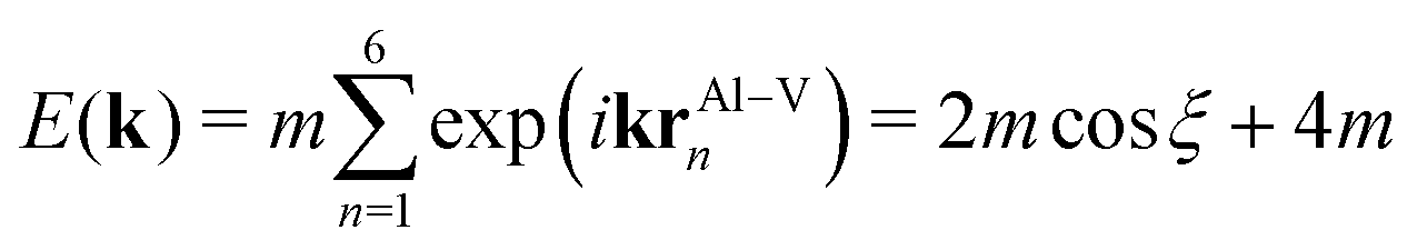 | (1) |
| E(ξ) = α(1 + cosξ), | (2) |
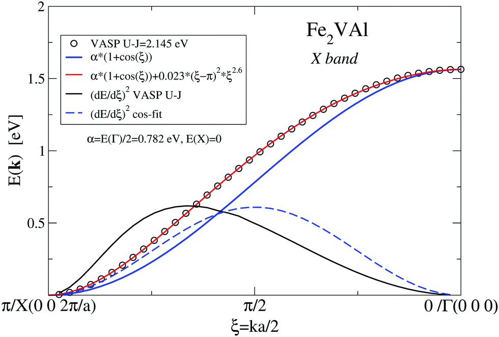 | ||
| Fig. 5 X band according to Fig. 4versus dimensionless parameter ξ. VASP results combined with two fits for the bands as well as band velocities (dE/dξ)2. | ||
Clearly, there is only moderate agreement with the VASP-derived data, although both bands start and end at the same energies. Coming from X, the VASP band starts with a steeper slope and ends with a less steep one at Γ. The different slopes are manifested by the different band velocities squared, (d(E)/dξ)2 as shown in Fig. 5. The band velocities are of great importance for transport properties as they appear explicitly in the calculation of the Seebeck coefficient and electrical resistivity (see eqn (3)). The cosine-like band can be optimized by adding a ξ- or k-dependent correction 0.023(ξ − π)2ξ2.6, which reduces the maximum deviation from the VASP results to less than 2 × 10⁻⁴ eV. The introduction of k-dependent corrections to the constant matrix elements indicates that the kinetic energy dominates the bond energy, which might suggest that the involved electronic states are of a confined-electron-gas-like character.
Whereas the E2-like character of the DOS (as discussed above) suggests bands linear in k, the analytic form of the discussed X band in Fig. 5 has a more complicated character.
The Γ bands in Fig. 4 originate from tails of xy, xz, and yz orbitals of Fe dangling towards the nearest Al. Sitting at the Al site, the nearest Fe atoms are found at the distances rAl–Fe = {(±a/4, ±a/4, ±a/4)} forming the corners of a cube. The formation of the bonding tails surrounding Al is similar to the X band, but more diffuse, as the xy, xz, and yz orbitals do not point directly at the origin of the cube. These bands start to cross other band manifolds at −0.3 eV, much earlier than the crossing of the X band.
Nevertheless, the parts of the Γ bands with large dispersions in combination with the X band are nearly exclusively responsible for the electronic transport properties up to high temperatures of at least 750 K.
In order to illustrate the previously mentioned situation where tails of the wave function of Fe and V dangle towards the Al site, we show contours of constant charge density. This is done for one of the threefold-degenerate Γ bands (Fig. 6) and for the X band (Fig. 7). The selected constant charge density is very small and in both cases attributed to 3d-like states that are strongly localized at the Fe or V sites, respectively.
 | ||
| Fig. 6 Charge density contours at Γ for one of the states of the Γ band. Contours for a density value of 0.005−3. Fe and nearest-neighbour Al atoms in tetrahedral coordination to Fe are plotted. | ||
 | ||
| Fig. 7 Charge density contours for the X band. Contours for a density value of 0.005-3. V and nearest-neighbour Al atoms in octahedral coordination to V are connected. | ||
Concerning the Γ band, the Fe site is surrounded by four tetrahedrally coordinated Al and four tetrahedrally coordinated V nearest-neighbours. Fig. 6 shows a deformation of the charge density towards the Al neighbours. At the energy of the discussed state, there is no Al-like state available for a possible bonding with the Fe-3d-like state. Small patches of the constant charge density are clustered around the V positions. The analysis of the orbital-like character of this state shows that it is formed equally by Fe-dxz and -dyz orbitals with a sizeable amount of charge in the large Al sphere of radius 2.65 Å, which is a consequence of the 3d wave function, dangling into the Al sphere. When moving away from Γ, the Γ bands have negative dispersion. This is indicated by the deformation of tails towards Al and simulates fictitious Al–Fe bonds as discussed above.
A more detailed view in terms of charge density contours is provided in the ESI.†
The lowest state of the X band is of V-3d-like character and is strongly localized at the V site.
Fig. 7 shows very small charge density clouds at the Fe positions, although the eight Fe atoms are nearest-neighbours to V. Again, the density is deformed in direction to the Al at rAl–V = {(±a/2, 0, 0),(0, ±a/2, 0),(0, 0, ±a/2)} and no directional V–Al bonds are visible. Concerning the dispersion, the situation is reversed with respect to the Γ bands. Starting at the X point, the dispersion is now positive.
3.3 Transport properties
 | (3) |
 | (4) |
 | (5) |
The components of the electrical conductivity tensor σij are expressed by
| σij = e2K0,ij, | (6) |
 | (7) |
In the case of cubic symmetry, like for the present study, the Seebeck tensor becomes diagonal and has three equal diagonal components
 | (8) |
Similarly, the conductivity tensor then also consists of three equal components
| σii = e2K0,ii. | (9) |
Assuming a constant relaxation time, the components of the Seebeck coefficient Sii become independent of τ, whereas a free constant relaxation time remains for the resistivity. Furthermore, the products of band velocity components vivi are always positive in the case of cubic symmetry. Therefore, changes of sign of Sii only result from the expression (E(k) − μ)1, yielding a positive Seebeck coefficient for states below the chemical potential E(k) < μ and a negative Seebeck coefficient for states above the chemical potential E(k) > μ.
 | ||
| Fig. 8 Calculated Seebeck coefficient (tensor component Sxx for cubic Fe2VAl) versus temperature for GGA–PBE calculation and selected manual band shifts. Experimentally measured values are denoted by circles. | ||
 | ||
| Fig. 9 Calculated Seebeck coefficient (tensor component Sxx for cubic Fe2VAl) versus temperature for the GGA–PBE calculation and several U − J parameters of the LUD approach. Experimentally measured values are denoted by circles. | ||
Inspecting Fig. 8, it can be clearly seen that the GGA-PBE calculations result in a far too small |S(T)| over the whole temperature range, which is due to the cancellation of band contributions from below and above EF owing to the previously established overlap of X and Γ bands E(X) − E(Γ) = −0.164 eV. By manually shifting the conduction bands upwards in Fig. 8, the measured S(T) is nicely reproduced for a ΔE = 0.12 eV, corresponding to a still negative band gap of −0.044 eV. Increasing the shift up to 0.164 eV (or a positive gap of 0.8 meV), a large maximum of S(T) = 130 μV K−1 is reached and the calculated S(T) still shows the same basic features. An abrupt change to large negative values of S(T) occurs for a further very small change of ΔE by 0.001 eV to 0.165 eV. Interestingly, S(T) for ΔE = 0.164 eV compares favourably with the LUD results for U − J = 2.145 eV in Fig. 9, which also show a sensitive dependency on the choice of the parameter U − J, i.e. the gap size.
The rather abrupt crossover from positive to negative values is typical for S(T) at a fixed temperature, when the chemical potential μ (note EF = μ(0)), residing in the valence band regime, increases and passes through a gap, residing then in the conduction band regime. In the study above, this crossover of S(T) happens, when a gap begins to form. At ΔE = 0.164 eV the gap is zero and becomes positive for larger shifts; for ΔE = 0.165 eV it is 0.001 eV. Inspecting eqn (3) and the definition of S(T) according to eqn (7), one realizes that states with energies  give a positive and states with
  a negative contribution to S(T). Summing now over all states by integrating over the entire
  -space, the sign of the total S(T) depends on the weight of each electronic state multiplied by the respective band velocities vi(k)vj(k) (which for cubic symmetry is positive definite). In our case, the sign of S(T) becomes negative when changing from ΔE = 0.164 eV to ΔE = 0.165 eV which is accompanied by a small jump of μ amounting to Δμ = 27 meV at 300 K. The chemical potential is now moved into the conduction band regime, because the DOS at energies below EF is larger than above EF as shown in Fig. 2. At T > 0 the Fermi–Dirac function is symmetrically smeared out around μ and becomes smaller than 1 for states with energies below the chemical potential (states are lost) and larger than 0 for states with energies above (states are gained). Because of charge neutrality, gains and losses must be of the same size, and for that, more states above EF are needed than below EF. Therefore EF shifts to the larger value of μ at the given temperature and S(T) becomes negative.
Fig. 9 shows results for the calculated temperature-dependent Seebeck coefficient S(T) for a standard GGA–PBE calculation and a set of LUD calculations with selected U − J parameters, in comparison with measured values. Compared to the present measurement, it is clearly apparent that the GGA–PBE calculation results in a far too small S(T) at T < 500 K. While the experimental S(T) becomes negative at 730 K, the GGA–PBE-calculated curve changes its sign at 773 K.
Searching for improvement of the calculated data of S(T), we applied a large number of LUD calculations, scanning the U − J parameter range for Fe from 0 to 4 eV. Fig. 9 shows that approaching U − J = 2.145 eV from lower energies broadens the positive narrow peak with its maximum below 200 K until 2.145 eV is reached.
We suggest to accept this value as the best choice in comparison to the present experiment, as the corresponding calculated S(T) has important features, which agree with the measured values, namely a maximum at 200 K and a change of sign at 730 K. Even small deviations of U − J from 2.145 eV (for example U − J = 2.15 and 2.139 eV) lead to significant modifications, which indicate the extreme sensitivity of S(T) on the relative position of the Γ bands and the X band. For the choice of U − J = 2.145 eV, the band gap E(X) − E(Γ) = −0.0093 eV is still negative but close to zero.
Here, it should be noted that three decimal digits for the U − J value do not mean that the presented procedure results in such a precise U − J. The value U − J = 2.145 eV should rather indicate that tiny variations in the U − J value may lead to sizeable changes of S(T) as indicated in Fig. 9.
For the optimized U − J = 2.145 eV, the disagreement with experiment is considerably high and the calculated maximum value of S is almost twice as large. One should be aware that the applied LUD approach is the most simplest concept for including strong correlation effects, going beyond DFT for Fe-d states. V-d states, which are presumably less but still strongly localized, are not included. Doing that, a second U − J parameter is introduced, which would largely increase the number of DFT calculations, scanning now for two parameters. We propose further investigations along this line and also by including more elaborate functionals and many-body interactions, for deriving the thermoelectric properties of Fe2VAl. Furthermore, the constant-relaxation time approach as defined in eqn (3), may cause deviations of the calculated values from the experimental ones, particularly at larger temperatures, at which also the influence of lattice vibrations may become important.
From the extensive DFT analysis of the temperature-dependent Seebeck coefficient S(T), varying the U − J parameters and applying manual band shifts, we conclude that the electronic structure of Fe2VAl should have a very small negative gap.
Fig. 10 shows the decomposition of the total Seebeck coefficient into the contributions from below and above the Fermi energy S(T) = Sabove + Sbelow. As established in eqn (7), Sabove is of negative sign for all temperatures, whereas Sbelow is always positive. Concerning the GGA–PBE calculation, this splitting yields two nearly linear curves of opposite sign, which almost cancel each other out, thus resulting in a very small total S(T).
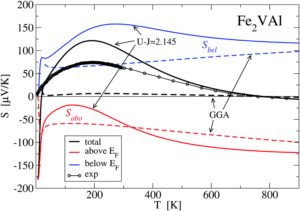 | ||
| Fig. 10 Calculated Seebeck coefficient (tensor component Sxx for cubic Fe2VAl) derived by the GGA–PBE (dashed lines) and the LUD approach with U − J = 2.145 eV for Fe 3d states (full lines). The total S(T) is splitted into contributions from below (Sbel) and above (Sabo) Fermi energy. | ||
The behaviour of S(T) is drastically changed when the parameter U − J = 2.145 eV is taken into account. Both contributions now exhibit a more complex behaviour with maxima around 100–300 K, which determine the maximum at T ≈ 200 K of the total Seebeck coefficient. Additionally, Sabove decreases faster than Sbelow at higher temperatures which leads to the change of sign of the total S(T) at ≈770 K.
 | ||
| Fig. 11 Calculated resistivity (component ρxx for cubic Fe2VAl) derived by the GGA–PBE calculation (dashed lines) and the selected manual energy shifts. All calculations are set equal to the measured value at 280 K. Experimental values are indicated by open circles. The solid line is the result of a least squares fit according to the phenomenological model of ref. 12, with a gap width ΔE = 0.057 eV. | ||
Employing a phenomenological two-band model based on a rectangular density of states (for details see ref. 12), one can model the experimental data quite accurately. The solid line in Fig. 11 is a least squares fit to the experimental data, where the gap of the box-like density of states is evaluated as ΔE = 0.057 eV. This value, although positive, is sufficiently small to be comparable to the present DFT results.
Fig. 12 compares the experimentally measured resistivity ρ(T) to several calculated LUD results. The relaxation time in the calculations was again chosen such that the obtained values are equal to the measured resistivity value at T = 280 K. Above 280 K the calculated data describe the experimental trend of a decreasing ρ(T) reasonably well. At T < 280 K the calculated resistivities vary strongly with the parameter U − J. The recommended value U − J = 2.145 eV yields significantly lower values of ρ than the other two shown LUD results with U − J = 2.5 eV and 2.138 eV, respectively.
 | ||
| Fig. 12 Calculated resistivity (component ρxx for cubic Fe2VAl) derived by the GGA–PBE calculation (dashed lines) and three LUD approaches (solid lines). All calculations are set equal to the measured value at 280 K. Experimental values are indicated by open circles. | ||
The standard GGA–PBE calculation shows the least agreement and particularly deviates from the experimental data at elevated temperatures. Nevertheless, the general trend of a decreasing ρ(T) with increasing T is present in all calculations, which is quite unusual for a metallic system. In all cases the DFT-derived gaps are negative and close to zero.
As already noted, the above-mentioned modeling of the temperature-dependent resistivity has some limitations. Considering a temperature and frequency-dependent relaxation time τ0 in eqn (10) could give further corrections to the DFT derived behaviour of ρ(T). For example, the interaction of electrons with long-wave length acoustic phonons, as already discussed Bardeen and Shockley,51 results in τ0 ∝ T−3/2. The scattering due to alloying and disorder in the crystal, on the other hand, yields τ0 ∝ T−1/2 (compare e.g., ref. 52). In fact, a recent study53 shows that the temperature-dependent Hall mobility of Fe2VAl at T > 300 K can be quite accurately modelled by considering these types of scattering mechanisms.
In general, the temperature-dependent electronic transport of semiconducting-like materials can be quite accurately modeled by considering only a few parabolic bands. Theoretical expressions for quantities like the Seebeck coefficient, the Lorentz number, the carrier density, the Hall factor or the electrical conductivity based on a single parabolic band have previously been developed (see e.g.ref. 54).
Within this framework, scattering processes are accounted for by a distinct scattering exponent λ in the context of the energy-dependent relaxation time, which can be expressed by a power law
| τ = τ0Eλ–1/2. | (10) |
Here, τ0 is a material dependent constant and E is the electron energy. λ = 0 for acoustic phonon scattering and λ = 1/2 for scattering of electrons on neutral impurities as well as grain boundaries.
In this scope, the Seebeck coefficient of an individual parabolic band, Si can be expressed as
 | (11) |
 . Fj(η) is the Fermi integral,
 | (12) |
In the case of Fe2VAl, we showed that one conduction band at X and multiple valence bands at Γ contribute to the electronic transport. The total Seebeck coefficient for a general number of N bands can be expressed as a sum of its single-band contributions Si weighted by the respective electrical conductivities σi
 | (13) |
By least squares fitting eqn (13) to the experimental data, parameters like the relative Fermi energy, the band gap and the relative effective masses can be obtained, allowing one to construct a simplified picture of the band structure.
Fig. 13 shows the temperature-dependent Seebeck coefficient for Fe2VAl evaluated within a parabolic three-band (3PB) model. Based on Fig. 4, a set of two valence bands (corresponding to states around Γ) and one conduction band (corresponding to states around X) are selected. Least squares fits of eqn (11) to (13) (solid line) to the experimental data (open and closed circles) were obtained, using the software package Mathematica, revealing convincing agreement. The deduced relative Fermi energy is located about 0.04 eV below the top of the valence band and the band gap between the two Γ valence bands and the X conduction band is calculated as 0.003 eV. If the energy separation between the two valence bands is not confined to the purely degenerate case of ΔEv = 0, the value of the gap can become slightly negative, down to −0.03 eV, as shown in ref. 53. This substantiates an almost zero or slightly negative band gap for Fe2VAl and affirms the recommended DFT+U-derived value of −0.0093 eV. A tiny positive band gap for Fe2VAl of the order of 0.03 eV was recently evaluated from a parabolic two-band model by Anand et al.,55 allowing to fairly well trace the temperature-dependent Seebeck coefficient in a limited temperature range. As a valuable advance, the presently applied 3PB model allows to accurately fit the experimental S(T) data in the entire temperature range.
 | ||
| Fig. 13 Temperature-dependent Seebeck coefficient for Fe2VAl simulated within a parabolic three-band (3PB) model. The open and closed circles are the experimental data. The solid line is a least squares fit and the inset sketches the band structure as derived from the fit parameters of the 3PB model. | ||
Another qualitative agreement with the DFT band structure in Fig. 4 is apparent when comparing the relative effective masses. Assuming the effective mass of the first parabolic valence band is 1 me, the effective mass of the second valence band is calculated as 0.6 me and m* = 0.22 me is found for the conduction band, with me being the free electron mass.
The steeper slope of the DOS below the Fermi energy (see Fig. 3) corroborates the heavier and flatter valence bands, while the less steep slope of the DOS above EF (Fig. 3) indicates a larger dispersion, which corresponds to the narrower parabolic conduction band. In the context of both, the DFT calculations and the parabolic band model, one may conclude that Fe2VAl is located right at the border between a semimetal and an indirect semiconductor. Slight shifts in stoichiometry of real samples, as well as antisite occupations of the various constituting elements on the four different sublattices of the cubic L21 Heusler phase can cause distinct modifications of the real band structure, too.
4 Summary and conclusion
In order to evaluate and understand the electronic structure and transport properties of Fe2VAl and its pseudogap states, extensive DFT-based calculations were performed. The nature of the band gap – pseudo- or real indirect gap – has brought up lots of questions in the past and many ambiguous results have been reported so far. There are numerous theoretical studies on Fe2VAl enforcing a real gap by applying parameter-dependent approaches such as DFT+U methods and advanced hybrid functionals. By employing the DFT+U approach of Dudarev et al.,36 we argue, on the basis of our modeling of S(T), that it is mandatory to have a very small negative or almost zero gap in the renormalized Kohn–Sham energy spectrum. The large negative gap of −0.164 eV found by standard GGA–PBE calculations cannot explain the temperature-dependent transport properties such as the Seebeck coefficient S(T) and the electrical resistivity ρ(T). These properties are nearly exclusively governed by the pseudogap states. By extensively scanning values of U − J for Fe-d-like states within the mentioned DFT+U approach, a value of U − J = 2.145 eV is suggested, resulting in a very small negative gap of E(X) − E(Γ) = −0.0093 eV. This very small negative gap might be even further reduced when spin–orbit coupling is taken into account.24 We found that the derived transport properties are very sensitive on the choice of the parameter U − J, i.e., the E(X) − E(Γ) separation.We propose an understanding of the nature of the pseudogap states in Fe2VAl. Firstly, there is a remarkable electronic charge transfer of 0.75 electronic charges per Fe atom from Al and to a lesser extent from V to the Fe atoms, as derived by Bader's approach.44–47 Secondly, a sizeable major gap of about 0.7 eV appears in the DOS between highly localized states. Thirdly, within this major gap, there arise peculiar pseudogap states with large dispersions that govern the temperature-dependent transport. These pseudogap states are created by tails of otherwise strongly localized Fe- and V-d states dangling towards the Al site. A set of four bands of such character appears, featuring three bands centered at Γ with a downward dispersion and one band centered at X with an upward dispersion. As an example, we formulated a tight-binding-based energy dispersion with k-dependent matrix elements for the pseudogap state band dispersing from X to Γ.
The calculated Seebeck coefficient and resistivity resulting from this DFT-picture of the band structure agree reasonably well with the key features of the measured S(T) and ρ(T) data. Our conclusions are also reinforced by phenomenological models that were least squares fitted to the experimental data. We anticipate that our work will grant new insights regarding the interplay between the band structure and the temperature-dependent transport properties within this type of compounds.
Conflicts of interest
There are no conflicts to declare.Acknowledgements
Research supported by the Christian Doppler Laboratory for Thermoelectricity and the JST Mirai JPMJMI19A1. DFT and related calculations were performed on the Vienna Scientific Cluster VSC3.Notes and references
- C. Felser and A. Hirohata, Heusler Alloys: Properties, Growth, Applications, Springer International Publishing, 2016 Search PubMed.
- Y. Nishino, S. Deguchi and U. Mizutani, Phys. Rev. B: Condens. Matter Mater. Phys., 2006, 74, 115115 CrossRef.
- Y. Nishino, J. Jpn. Soc. Powder Powder Metall., 2010, 57, 201–206 CrossRef CAS.
- M. Mikami, Y. Kinemuchi, K. Ozaki, Y. Terazawa and T. Takeuchi, J. Appl. Phys., 2012, 111, 093710 CrossRef.
- N. Tsujii, A. Nishide, J. Hayakawa and T. Mori, Sci. Adv., 2019, 5, eaat5935 CrossRef CAS.
- B. Hinterleitner, I. Knapp, M. Poneder, Y. Shi, H. Müller, G. Eguchi, C. Eisenmenger-Sittner, M. Stöger-Pollach, Y. Kakefuda, N. Kawamoto, Q. Guo, T. Baba, T. Mori, S. Ullah, X.-Q. Chen and E. Bauer, Nature, 2019, 576, 85–90 CrossRef CAS.
- B. Hinterleitner, P. Fuchs, J. Rehak, F. Garmroudi, M. Parzer, M. Waas, R. Svagera, S. Steiner, M. Kishimoto, R. Moser, R. Podloucky and E. Bauer, Phys. Rev. B, 2020, 102, 075117 CrossRef CAS.
- S. Maier, S. Denis, S. Adam, J.-C. Crivello, J.-M. Joubert and E. Alleno, Acta Mater., 2016, 121, 126–136 CrossRef CAS.
- H. Al-Yamani and B. Hamad, J. Electron. Mater., 2016, 45, 1101–11014 CrossRef CAS.
- M. Khalfa, H. Khachai, F. Chiker, N. Baki, K. Bougherara, A. Yakoubi, G. Murtaza, M. Harmel, M. S. Abu-Jafar, S. B. Omran and R. Khenata, Int. J. Mod. Phys. B, 2015, 29, 1550229 CrossRef CAS.
- S. S. Shastri and S. K. Pandey, Comput. Mater. Sci., 2018, 143, 316–324 CrossRef CAS.
- I. Knapp, B. Budinska, D. Milosavljevic, P. Heinrich, S. Khmelevskyi, R. Moser, R. Podloucky, P. Prenninger and E. Bauer, Phys. Rev. B, 2017, 96, 045204 CrossRef.
- M. Weinert and R. Watson, Phys. Rev. B: Condens. Matter Mater. Phys., 1998, 58, 9732–9740 CrossRef CAS.
- M. Kato, Y. Nishino, S. Asano and S. Ohara, J. Jpn. Inst. Met., 1998, 62, 669–674 CrossRef CAS.
- K. Soda, H. Murayama, K. Shimba, S. Yagi, J. Yuhara, T. Takeuchi, U. Mizutani, H. Sumi, M. Kato, H. Kato, Y. Nishino, A. Sekiyama, S. Suga, T. Matsushita and Y. Saitoh, Phys. Rev. B: Condens. Matter Mater. Phys., 2005, 71, 245112 CrossRef.
- Y. Nishino, M. Kato, S. Asano, K. Soda, M. Hayasaki and U. Mizutani, Phys. Rev. Lett., 1997, 79, 1909–1912 CrossRef CAS.
- C. S. Lue, J. H. Ross, C. F. Chang and H. D. Yang, Phys. Rev. B: Condens. Matter Mater. Phys., 1999, 60, R13941–R13945 CrossRef CAS.
- A. Berche, M. Noutack, M.-L. Doublet and P. Jund, Mater. Today Phys., 2020, 13, 100203 CrossRef.
- S. Bandaru and P. Jund, Phys. Status Solidi B, 2017, 254, 1600441 CrossRef.
- S. Bandaru, A. Katre, J. Carrete, N. Mingo and P. Jund, Nanoscale Microscale Thermophys. Eng., 2017, 21, 237–246 CrossRef CAS.
- D. I. Bilc and P. Ghosez, Phys. Rev. B: Condens. Matter Mater. Phys., 2011, 83, 205204 CrossRef.
- D. Do, M.-S. Lee and S. Mahanti, Phys. Rev. B: Condens. Matter Mater. Phys., 2011, 84, 125104 CrossRef.
- O. Kristanovski, R. Richter, I. Krivenko, A. I. Lichtenstein and F. Lechermann, Phys. Rev. B, 2017, 95, 045114 CrossRef.
- R. Weht and W. Pickett, Phys. Rev. B: Condens. Matter Mater. Phys., 1998, 58, 6855–6861 CrossRef CAS.
- D. J. Singh and I. Mazin, Phys. Rev. B: Condens. Matter Mater. Phys., 1998, 57, 14352–14356 CrossRef CAS.
- J. M. Tomczak, J. Phys.: Condens. Matter, 2018, 30, 183001 CrossRef.
- C. S. Lue, C. F. Chen, J. Y. Lin, Y. T. Yu and Y. K. Kuo, Phys. Rev. B: Condens. Matter Mater. Phys., 2007, 75, 064204 CrossRef.
- M. Mikami and K. Kobayashi, J. Alloys Compd., 2008, 466, 530–534 CrossRef CAS.
- M. Mikami, S. Tanaka and K. Kobayashi, J. Alloys Compd., 2009, 484, 444–448 CrossRef CAS.
- K. Renard, A. Mori, Y. Yamada, S. Tanaka, H. Miyazaki and Y. Nishino, J. Appl. Phys., 2014, 115, 033707 CrossRef.
- M. Mikami, M. Inukai, H. Miyazaki and Y. Nishino, J. Electron. Mater., 2016, 45, 1284–1289 CrossRef CAS.
- P.-C. Wei, T.-S. Huang, S.-W. Lin, G.-Y. Guo and Y.-Y. Chen, J. Appl. Phys., 2015, 118, 165102 CrossRef.
- H. Al-Yamani and B. Hamad, J. Electron. Mater., 2016, 45, 1101–1114 CrossRef CAS.
- S. Masuda, K. Tsuchiya, J. Qiang, H. Miyazaki and Y. Nishino, J. Appl. Phys., 2018, 124, 035106 CrossRef.
- F. Garmroudi, M. Parzer, A. Riss, N. Reumann, B. Hinterleitner, H. Müller, K. Tobita, Y. Katsura, K. Kimura, T. E. Mori and E. Bauer, submitted.
- S. L. Dudarev, G. A. Botton, S. Y. Savrasov, C. J. Humphreys and A. P. Sutton, Phys. Rev. B: Condens. Matter Mater. Phys., 1998, 57, 1505–1508 CrossRef CAS.
- S. Bandaru and P. Jund, Phys. Status Solidi B, 2017, 254, 1600441 CrossRef.
- G. Kresse and J. Furthmüller, Comput. Mater. Sci., 1996, 6, 15–50 CrossRef CAS.
- G. Kresse and J. Furthmüller, Phys. Rev. B: Condens. Matter Mater. Phys., 1996, 54, 11169–11186 CrossRef CAS.
- P. E. Blöchl, Phys. Rev. B: Condens. Matter Mater. Phys., 1994, 50, 17953–17979 CrossRef.
- G. Kresse and D. Joubert, Phys. Rev. B: Condens. Matter Mater. Phys., 1999, 59, 1758–1775 CrossRef CAS.
- J. P. Perdew and Y. Wang, Phys. Rev. B: Condens. Matter Mater. Phys., 1992, 45, 13244–13249 CrossRef.
- G. K. Madsen and D. J. Singh, Comput. Phys. Commun., 2006, 175, 67–71 CrossRef CAS.
- R. Bader, Atoms in Molecules: A Quantum Theory, USA, Oxford University Press, 1994, pp. 1–454 Search PubMed.
- R. Bader, Encyclopedia Computat Chem, 1998, 1, 6486 Search PubMed.
- W. Tang, E. Sanville and G. Henkelman, J. Phys.: Condens. Matter, 2011, 21, 084204 CrossRef.
- M. Yu and D. R. Trinkle, J. Chem. Phys., 2011, 134, 064111 CrossRef.
- F. Failamani, R. Podloucky, J. Bursik, G. Rogl, H. Michor, H. Müller, E. Bauer, G. Giester and P. Rogl, Dalton Trans., 2017, 47, 3303–3320 RSC.
- J. Slater and G. Koster, Phys. Rev., 1954, 94, 1498–1524 CrossRef CAS.
- M. X. Chen and R. Podloucky, Phys. Rev. B: Condens. Matter Mater. Phys., 2013, 88, 045134 CrossRef.
- J. Bardeen and W. Shockley, Phys. Rev., 1950, 80, 72–80 CrossRef CAS.
- S. Krishnamurthy, A. Sher and A. Chen, Appl. Phys. Lett., 1985, 47, 160–162 CrossRef CAS.
- F. Garmroudi, A. Riss, M. Parzer, N. Reumann, H. Müller, E. Bauer, S. Khmelevskyi, R. Podloucky, K. Tobita, Y. Katsura and K. Kimura, Phys. Rev. B, 2021 Search PubMed , in press.
- A. May and G. Snyder, Introduction to modeling thermoelectric transport at high temperatures, CRC Press, 2017, pp. 11-1–11-18 Search PubMed.
- S. Anand, R. Gurunathan, T. Soldi, L. Borgsmiller, R. Orenstein and G. J. Snyder, J. Mater. Chem. C, 2020, 8, 10174–10184 RSC.
Footnote |
| † Electronic supplementary information (ESI) available: See DOI: 10.1039/d0tc05187j |
| This journal is © The Royal Society of Chemistry 2021 |