
Pentacene/non-fullerene acceptor heterojunction type phototransistors for broadened spectral photoresponsivity and ultralow level light detection†
Keli
Shi
*a,
Risheng
Jin
a,
Shihua
Huang
*a,
Hongwei
Lei
 d,
Pei
Dai
d,
Dan
Chi
a,
Weifeng
Zhang
*b and
Gui
Yu
*bc
d,
Pei
Dai
d,
Dan
Chi
a,
Weifeng
Zhang
*b and
Gui
Yu
*bc
aCollege of Physics and Electronic Information Engineering, Zhejiang Normal University, Zhejiang 321004, P. R. China. E-mail: shikl@zjnu.edu.cn; huangshihua@zjnu.cn
bBeijing National Laboratory for Molecular Sciences, Institute of Chemistry, Chinese Academy of Sciences, Beijing 100190, P. R. China. E-mail: zhangwf@iccas.ac.cn; yugui@iccas.ac.cn
cSchool of Chemical Sciences, University of Chinese Academy of Sciences, Beijing 100049, P. R. China
dCollege of Science, Huazhong Agricultural University, Wuhan 430070, P. R. China
First published on 17th November 2020
Abstract
ITIC-type non-fullerene acceptors (NFAs) have attracted substantial attention in organic photovoltaics due to their advantages over fullerene derivative molecules. Briefly, the strengthened absorption coefficient, broadened spectral photoresponse, efficient exciton dissociation as well as tunable energy levels of ITIC-NFAs make them competitive components for organic optoelectronics. Here, a high-performance organic phototransistor is displayed using a simple bi-layer heterojunction of pentacene and ITIC. As a high performing semiconductor, pentacene serves as the p-type channel to transport the photo-generated carriers. Meanwhile, the representative NFA molecule, ITIC, is first applied in the organic heterojunction phototransistors (OHPTs) to improve the light detection range by extending the absorption into NIR and to enhance the light detection limit (0.3 μW cm−2). The maximum values of photoresponsivity (R), Iphoto/Idark ratio and external quantum efficiency (EQE) are up to 1.0 × 10⁵ A W−1, 4.7 × 10⁵ and 2.0 × 10⁵%, respectively. The overall performances of our device are among the highest values in all-organic thin-film heterojunction phototransistors. These results demonstrate that ITIC-type NFAs could be highly efficient alternative acceptors for high-performance OHPTs.
Introduction
Organic electronic devices have attracted much attention due to their low cost, flexibility and ease of processing.1,2 In particular, organic photodetectors can convert light signals into electric signals, thus having broad applications in healthcare, environmental monitoring, secure communication, radiation detection and other fields.3–6 Among all types of organic photodetectors, organic photodiodes (OPDs) and organic phototransistors (OPTs) are the most commonly investigated.7 The performance of OPTs can be modulated using both the incident light and the gate voltage applied. Compared to two terminal OPDs, three terminal OPTs have the following distinctions:8–13 (1) OPTs have higher flexibility of working modes. Its sensitivity and dark current can be controlled using a gate field-effect to achieve greater functionality in a single device such as signal amplification. (2) They have a simple active circuit design as a result of a three terminal structure. (3) In some cases, the phototransistors can integrate charge storage and photodetection functions into a single device, which can be applied to imagers, scanners and detectors. In addition, phototransistors can detect ultraweak light owing to their very high responsivity. And ultraweak light detectors have wide-ranging important applications in astronomical observation, quantum communication, remote sensing, cryptography, etc.10The high photodetectivity of conventional OPTs usually relies on their high carrier mobility, efficient light absorption and exciton dissociation of the channel materials.14 Efforts have been made to design and synthesize new organic molecules for the channel materials of OPTs; however, organic molecules that deliver high mobility and good photodetectivity simultaneously are relatively limited.15 In addition, the performances of OPTs can also be improved through the optimization of fabrication methods, such as single-crystal organic phototransistors and inorgainc quantum dots or Au nanoparticle decorated organic phototransistors and so on.9,12,14 However, most of them are expensive, complicated and less scalable for mass production.9,16,17 Therefore, there is an urgent need to develop OPTs with simple processing and high photosensitivity. One of the effective protocols is the usage of a simple donor/acceptor (D/A) heterojunction with enhanced photosensitivity in OPTs.7,8,18–25 Up to now, a wide variety of donor organic semiconductors as photoconductors have been investigated, yet organic semiconductor acceptors are mainly limited to a few fullerene derivatives, such as PC61BM or PC71BM.10,20,26–30 A challenge in fullerene derivatives is insufficient visible absorption due to their wide bandgaps,31 but photodetectors with broad bandwidth response are critical for a variety of industrial and scientific applications. Moreover, chemical functionalization of fullerenes has little effect on reducing their bandgaps.31,32 Furthermore, spherically structured PCBM easily crystallize and aggregate, which reduces the D/A interface and the long-term stability of devices, especially for the devices with a heterojunction structure. Hence, it is necessary to search an alternative acceptor that combines strong broadband absorption and chemical functionalization for organic heterojunction phototransistors (OHPTs) with high responsivity and weak signal detection.
Over the past four years, the rapid development of non-fullerene acceptors (NFAs) has resulted in providing effective ways to overcome these challenges. In 2015, Zhan et al. synthesized a model NFA, ITIC, which can work well with many donors.32 Since then a number of novel NFAs have been designed and synthesized by the structural modifications of ITIC, such as ITIC-Th, ITIC2, IDIC and so on, which can be called ITIC-type NFAs.31–35 ITIC-type NFAs represent a new generation of electron-accepting small molecules for organic photovoltaic (OPV) applications. The breakthrough of ITIC-type NFAs can be attributed to several factors. First, the energy levels of ITIC-type NFAs allow appropriate alignment with many electron donor materials due to their high electron affinity, resulting in a strong tendency to accept electrons from donor and enhanced charge separation efficiency. Second, ITIC-type NFAs also have strong and broad absorption characteristics that even widen to the NIR region.32,33,36 So far, many reported organic photovoltaic diodes with high photon-to-electron conversion are based on ITIC-type NFAs. In addition, Zhang et al. reported the two terminal photomultiplication (PM) type OPDs.37 According to previous studies, the important ways for improving the performance of OHPTs are to upgrade the capability of photon-to-electron conversion, the charge-trapping effect and charge transport efficiency of the active layer, which indicate that ITIC-type NFAs have potential as electron acceptor materials to fabricate OHPTs with ultra-high photosensitivity and broad bandwidth response.14,37–39 However, compared to the attention received by two terminal OPV devices and PM type OPDs, the role ITIC-type NFAs plays in three terminal OHPTs has scarcely been investigated so far. Organic field-effect transistors based on pentacene have a high Ion/Ioff ratio, high hole mobility and good air stability, which can provide fast transportation paths for the photogenerated charges.40–43 Due to the large absorption efficiencies of ITIC, the relatively high charge mobility and stability of pentacene, it is feasible to integrate pentacene with ITIC-type NFAs for the development of OHPTs that simultaneously exhibit ultra-high photosensitivity and broad bandwidth response. To the best of our knowledge, ITIC-type NFAs are used for the first time as electron acceptors in the fabrication of high-performance OHPTs.
Here, we report a phototransistor based on a bi-layer heterojunction of ITIC and pentacene. The phototransistor not only has higher carrier mobility and lower dark current, but also possesses ultrahigh detectivity in the range of 365 to 750 nm and ultralow illumination (0.3 μW cm−2). The OHPT exhibited excellent performance with photoresponsivity (R) of 1.0 × 10⁵ A W−1, Iphoto/Idark ratio of 4.7 × 10⁵ and external quantum efficiency (EQE) of 2.0 × 10⁵%. More importantly, the OHPT based on ITIC/pentacene can store the light information over a long time of 10![[thin space (1/6-em)]](https://www.rsc.org/images/entities/char_2009.gif) 000 s. The overall performances of our device are among the highest values of all-organic heterojunction thin-film phototransistors (Table S1, ESI†).19,20,23,25–27,44–47 All the measurements were carried out under ambient conditions. These results demonstrate that ITIC-type NFAs could be highly efficient alternative acceptors for high-performance OHPTs.
000 s. The overall performances of our device are among the highest values of all-organic heterojunction thin-film phototransistors (Table S1, ESI†).19,20,23,25–27,44–47 All the measurements were carried out under ambient conditions. These results demonstrate that ITIC-type NFAs could be highly efficient alternative acceptors for high-performance OHPTs.
Results and discussion
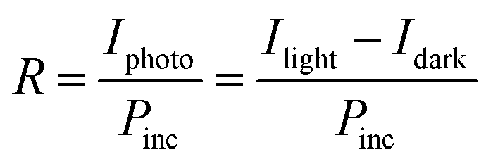
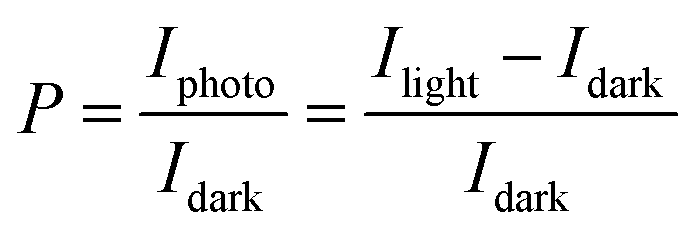
The device structure of the OHPT and the molecular structures of the ITIC and pentacene are shown in Fig. 1a–c, respectively. The ITIC/pentacene-based OHPT was fabricated on a heavily doped SiO2/n+-Si substrate with a bottom-gate/top-contact transistor geometry. To fabricate bi-layer heterojunction films, we deposited an ITIC layer on a SiO2 substrate by spin-coating, followed by vacuum evaporation of pentacene thin film on top of the ITIC surface. The thicknesses of the ITIC and pentacene layers are ∼35 and ∼40 nm, respectively. The detailed process of device fabrication is described in the experimental section. Fig. 1d displays the UV-vis absorption spectra of the ITIC, pentacene and ITIC/pentacene heterojunction films deposited on quartz substrates. The ITIC film exhibits strong absorption in the wavelength range of 500–800 nm and comparably weaker absorption in the wavelength range of 300–500 nm. It displays wide light absorption in the UV to NIR region, indicating its potential for broadband photodetection. On the contrary, pentacene film shows almost no evident absorption in the 700–800 nm region and its absorption intensity in the ultraviolet to NIR region is notably weaker than that of ITIC. The absorbance of the ITIC/pentacene heterojunction film displays a widened absorption range from 300 to 800 nm. Thus, ITIC enhances the absorption range of pentacene.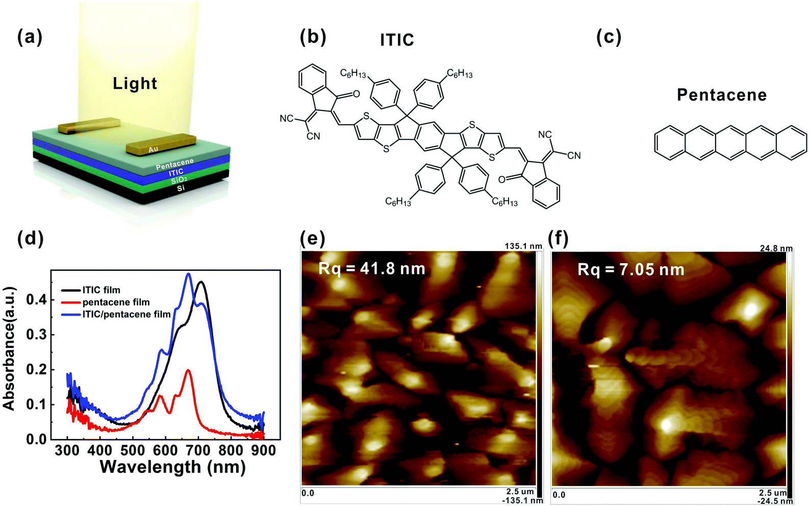 | ||
| Fig. 1 (a) Schematic diagram of the ITIC/pentacene heterojunction phototransistor. The molecular structures of (b) ITIC and (c) pentacene. (d) UV-vis absorption spectra of ITIC, pentacene and ITIC/pentacene heterojunction films. AFM height images of pentacene films on (e) SiO2 surface and (f) ITIC film. | ||
The typical transfer and output curves of the transistors based on pure pentacene and ITIC/pentacene in the dark are shown in Fig. S1 (ESI†). The saturation hole mobility and Ion/Ioff ratio of the pure pentacene-based transistor are 0.12 cm2 V−1 s−1 and ≈103, respectively (Fig. S1a and b, ESI†). In contrast, the mobility and Ion/Ioff ratio of the ITIC/pentacene-based transistor increase to 0.28 cm2 V−1 s−1 and ≈105, respectively (Fig. S1c and d, ESI†). Obviously, both the mobility and Ion/Ioff ratio of the ITIC/pentacene-based transistor are higher than those of the pure pentacene-based transistor in the dark. Particularly, the Ion/Ioff ratio of the ITIC/pentacene-based transistor is about 2 orders of magnitude higher than that of the pentacene-based transistor. The off-state current of the ITIC/pentacene-based transistor is down to 10−11 A, so it would be a good candidate and can be used in the phototransistor applications.7 The morphologies of the pentacene and pentacene/ITIC heterojunction films were measured using atomic force microscopy (AFM). Fig. 1e and f show their pronounced differences in average grain size, grain boundaries and surface roughness. Compared with the pentacene film deposited on the ITIC film, the pentacene film directly deposited on the SiO2 surface has smaller grain sizes, larger grain boundaries and higher roughness (Rq = 41.8 nm for pentacene film on the SiO2 surface and Rq = 7.05 nm for the pentacene/ITIC heterojunction film). Therefore, the reasons for off-state current suppression and mobility enhancement may be due to the reduction in the number of traps at the interface and the larger grain sizes of pentacene by inserting an ITIC layer between pentacene and SiO2.48 Nevertheless, at present, a majority of OHPTs employ a bulk heterojunction structure,7,10,20–25 in which the devices generally have lower device carrier mobilities and relatively high dark current due to the randomly distributed donor/accept interface, leading to low photodetectivity.25
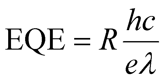
To evaluate the photodetectivity of the ITIC/pentacene-based OHPT, we measured the transfer characteristics of the device in the dark and under different light intensities. As shown in Fig. 1d, the strongest absorption band of both the ITIC and ITIC/pentacene films is in the range of 600–700 nm. Therefore, we investigated the photodetectivity and capability of ultraweak light detection at a suitable wavelength (630 nm). As shown in Fig. 2a, the transfer curves were characterized in the dark and under different light intensities at 630 nm. With the increase of illumination intensities, transfer curves shift to higher gate voltages and the source–drain current increases sharply. Moreover, we measured the transfer curves of the ITIC/pentacene-based phototransistors in the dark, under illumination and on removing the light as shown in Fig. S2 (ESI†). After removing the light, the transfer curve almost returns to its initial state. Calculated from the transfer curves in the dark and under different illumination intensities, we obtained two crucial parameters to assess the performances of the OHPT, namely, R and Iphoto/Idark ratio, according to the following equations:8
 | (1) |
 | (2) |
 | (3) |
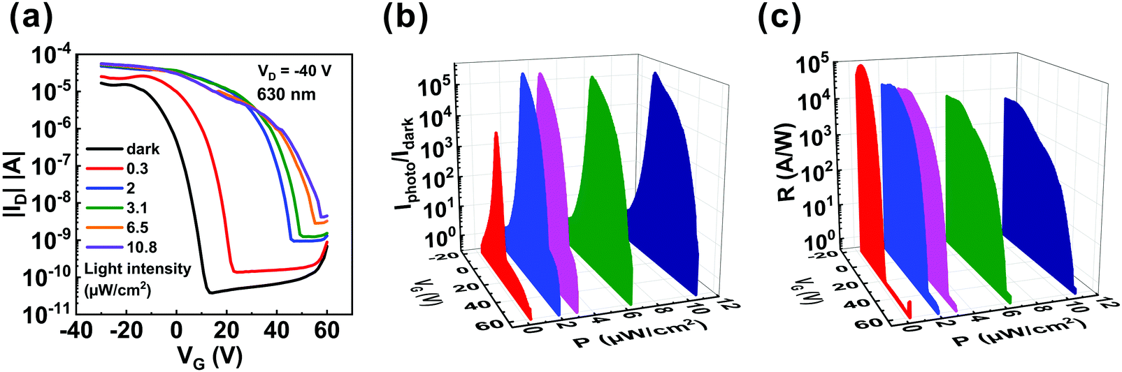 | ||
| Fig. 2 (a) Transfer characteristics of the phototransistors based on the ITIC/pentacene heterojunction under different illumination intensities at 630 nm. (b) Iphoto/Idark ratio and (c) photoresponsivity (R) of the phototransistors based on ITIC/pentacene under different illumination intensities at 630 nm at different gate voltages. | ||
According to the UV-vis absorption spectrum, we found that ITIC enhanced the absorption spectrum beyond 700 nm. To confirm that there is good photosensitivity in this region, the light detection of the OHPT was further studied under light illumination of 750 nm. The transfer curves of the phototransistors were measured in the dark and under different illumination intensities at VD = −40 V, as shown in Fig. 3a. It can be seen that the transfer curves shift to higher gate voltages with the increase in light intensities, and the minimum light intensity is still as low as 0.3 μW cm−2.
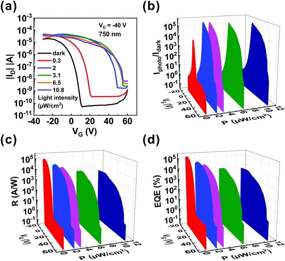 | ||
| Fig. 3 (a) Transfer characteristics of the phototransistors based on ITIC/pentacene heterojunction under different illumination intensities at 750 nm. (b) Iphoto/Idark ratio, (c) R and (d) EQE of the phototransistors based on the ITIC/pentacene heterojunction under different illumination intensities at 750 nm at different gate voltages. | ||
Fig. 3b depicts the gate voltage-dependent Iphoto/Idark ratio under different illumination intensities and the maximum Iphoto/Idark ratio is also over 105. Fig. 3c depicts the gate voltage-dependent R under different illumination intensities at 750 nm. The maximum R can be as high as ∼1.0 × 10⁵ A W−1 under an ultraweak light intensity of 0.3 μW cm−2. Fig. S8 (ESI†) shows the R and Iphoto/Idark of the phototransistors based on ITIC/pentacene heterojunction under various light intensities at 750 nm. We find that when the light intensity increases, the Iphoto/Idark ratio and R exhibit the same trend under light illumination of 630 nm. The highest EQE obtained from Fig. 3d reached to 1.8 × 10⁵%. The EQE (Vg = −9.6 V) of the phototransistor based on the ITIC/pentacene heterojunction under various light intensities at 750 nm is displayed in Fig. S9 (ESI†), and its value decreases as the light intensity increases. Furthermore, the pure pentacene sample was also characterized under light illumination of 750 nm as shown in Fig. S10 (ESI†). Similarly, compared with that of the phototransistors based on pure pentacene, the Iphoto/Idark ratio, R and EQE of the ITIC/pentacene-based phototransistors are significantly enhanced under light illumination of 750 nm. The excellent photodetectivity of the phototransistors based on the ITIC/pentacene heterojunction under light illumination of 750 nm is attributed to the strong absorption in the 700–800 nm region, efficient exciton dissociation and the high hole mobility in the ITIC/pentacene heterojunction thin film.
The broadband photoresponse of the device was further examined. Fig. 4 shows the transfer characteristics of the transistors based on the ITIC/pentacene heterojunction measured in the dark and under illuminations of λ = 365–750 nm (365, 470, 525, 630 and 750 nm). Note that the Iphoto/Idark ratios of the transistors based on the ITIC/pentacene heterojunction are all more than 104 under illuminations of their corresponding wavelengths (from 365 to 750 nm), which demonstrates that the transistor based on the ITIC/pentacene heterojunction has broad spectral photodetectivity.
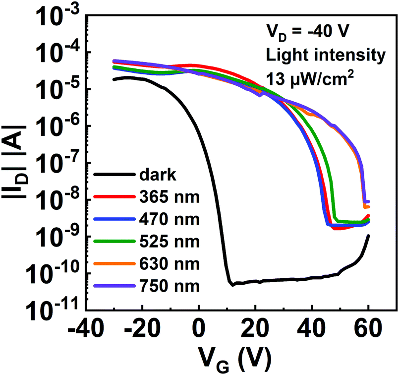 | ||
| Fig. 4 Transfer curves of the phototransistors based on the ITIC/pentacene heterojunction in the dark and under light illumination of different wavelengths with a light intensity of 13 μW cm−2. | ||
The transient photoresponsive behavior of the the pentacene/ITIC-based phototransistors was investigated during the on and off switching of light illumination. However, during this process, we found that just switching off the light illumination did not recover the photocurrent of the the pentacene/ITIC-based phototransistors to the off-state. In contrast, ID retains a high value and has almost no attenuation over a period of 10000 seconds even after the light illumination (light intensity = 6.5 μW cm−2) is turned off as shown in Fig. S11 (ESI†), which indicates that the trapped electrons remain in the thin film over a long time. The phenomenon is known as persistent photoconductivity (PPC).50 In order to further demonstrate the occurrence of charge storage in the the pentacene/ITIC-based phototransistors, double-sweep characteristics for both pentacene- and pentacene/ITIC-based phototransistors in the dark and under light illumination of 750 nm are shown in Fig. S12 (ESI†). The double-sweep transfer curves of pure pentacene-based phototransistors in Fig. S12a and b (ESI†) display almost no hysteresis loop as the voltage swept between the forward and reverse. On the contrary, in Fig. S12c and d (ESI†), the double-sweep transfer curves of the pentacene/ITIC-based phototransistors display an obvious hysteresis loop as the voltage swept between the forward and reverse, which is mainly due to the trapping and detrapping of charge carriers at the ITIC layer and ITIC/pentacene interface. These phenomena mentioned above demonstrate the occurrence of charge storage in the pentacene/ITIC-based phototransistors.8,11,51,52 Thus, a negative gate bias was applied to release the stored electrons and recombine the electron–hole, making the current return to the initial state. In Fig. 5a–e, the transient photoresponsive behaviors of the pentacene/ITIC-based phototransistors are shown under light illuminations of λ = 365–750 nm (365, 470, 525, 630 and 750 nm), respectively. There is no obvious change in the signal response during repeated light pulses and reset electrical pulses under the five given wavelengths (365, 470, 525, 630 and 750 nm), which shows that the OHPT had good reversibility and stability. Fig. 5f shows one transient photoresponse to reveal the process. As the ITIC/pentacene based OHPT is exposed to 750 nm light illumination, ID increases rapidly to the maximum. After the light is turned off, the on-state current retains a high value. It is completely erased by applying an additional negative gate voltage pulse (−80 V, 1 s). This process contains the “write” (light on), the “read-on” (the on-state current is maintained), the “erase” (−80 V gate voltage pulse), and the “read-off” (the off-state current after erasing) stages. The abovementioned results indicate that our OHPT integrates the photodetection and photo-memory properties within one single device. Moreover, recent study has shown that memory phototransistors are beneficial to realize ultraweak light detection, which also further explains that our OHPT has the ability of ultraweak light detection.53
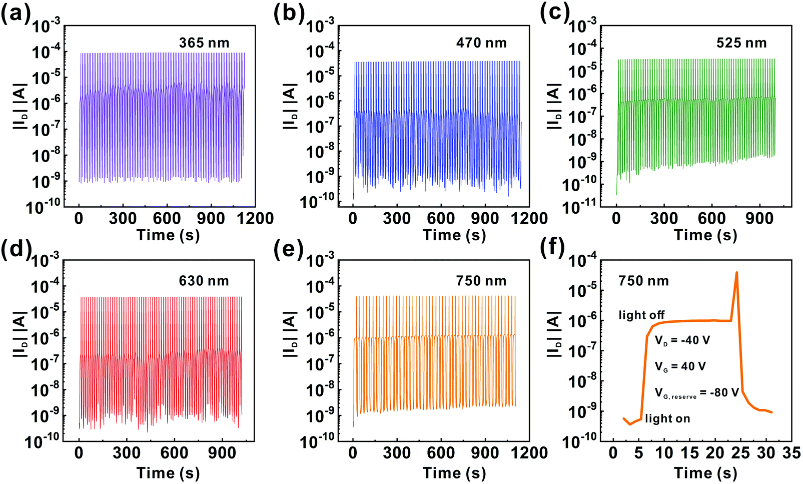 | ||
| Fig. 5 Photoswitching characteristics of the phototransistor based on the ITIC/pentacene heterojunction under alternating ON/OFF cycles under light illumination of the five given wavelengths: (a) 365 (13 μW cm−2), (b) 470 (13 μW cm−2), (c) 525 (13 μW cm−2), (d) 630 (13 μW cm−2) and (e) 750 nm (6.5 μW cm−2). (f) One transient photoresponse under light illumination of 750 nm (6.5 μW cm−2). | ||
Because the ITIC/pentacene-based phototransistor has broad spectral photodetectivity, in addition to studying the photodetection performances under various monochromatic lights, we explored the white light photodetection performance. As shown in Fig. S13a (ESI†), the transfer characteristics were characterized in the dark and under white light with different intensities at a fixed VD of −40 V. The ITIC/pentacene-based phototransistor also shows outstanding white light detection performance. The maximum values of the Iphoto/Idark ratio and R are up to 104 and 1.0 × 10⁵ A W−1, respectively, as shown in Fig. S13b and c (ESI†). Fig. S14 (ESI†) shows the transient photoresponsive behavior of the ITIC/pentacene-based phototransistor under white light illumination. We found that there was also no obvious change in the signal response during repeated light pulses and reset electrical pulses under white light.
To further study the operation mechanism of the ITIC/pentacene-based phototransistor, photoluminescence (PL) measurements were used to corroborate the mechanism governing the charge carrier transport.25 As shown in Fig. 6a, the PL intensity of the ITIC/pentacene thin film is less than that of the ITIC, which indicates the efficient charge carrier transfer between the ITIC and pentacene molecules. The energy band diagrams of the OHPT are shown in Fig. 6b.25,54,55 This staggered energy band alignment belongs to type II structure that is a highly favourable structure for exciton separation.56 In order to further verify the operation mechanism, another phototransistor based on ITIC and dioctylbenzothieno[2,3-b]benzothiophene (C8-BTBT) bi-layer heterojunction was prepared and its structure was the same as that of the ITIC/pentacene-based phototransistor. For comparison, an OFET based on pure C8-BTBT film was prepared. It hardly absorbs in the range of 400–800 nm,9 so the C8-BTBT based transistor exhibits poor photoresponse characteristics to 750 nm light as shown in Fig. S15a (ESI†). Nevertheless, the phototransistor based on the ITIC/C8-BTBT heterojunction film shows significant responses under light illumination of 750 nm due to the excellent absorption properties of the ITIC film as shown in Fig. S15b (ESI†). According to the results of the above experiments, the working principle of the ITIC/pentacene-based phototransistor is described in Fig. 6b. Under light illumination, large amounts of excitons are generated in the ITIC layer. The photoinduced excitons then diffuse to the ITIC/pentacene interface and dissociate to electrons and holes. The photoholes move from the HOMO of ITIC to the HOMO of pentacene, leading to the generation of a large photocurrent, and the photoelectrons are trapped in ITIC.8,57 Our strategy of the heterojunction phototransistor devices based on a new generation of NFAs can be applied for the fabrication of high-performance phototransistors.
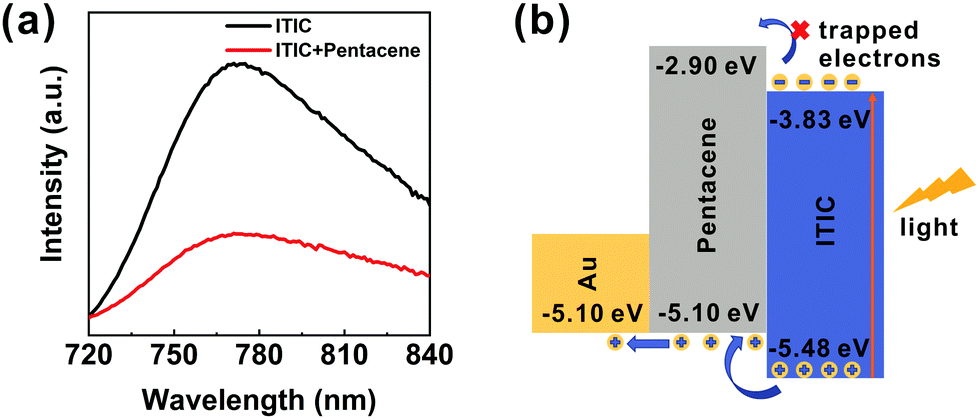 | ||
| Fig. 6 (a) PL spectra of both the bare ITIC and ITIC/pentacene hybrid thin films, and (b) energy level diagram of the ITIC/pentacene-based phototransistor under light illumination. | ||
Conclusion
In this work, a high-performance phototransistor with ultrahigh photosensitivity and broadband response was fabricated via a simple ITIC/pentacene bi-layer heterojunction. ITIC has strong broad-band absorption characteristic and superior charge separation efficiency. Meanwhile, pentacene can provide fast transport paths for the photo-generated charge carriers due to its high hole mobility. Because of the complementary properties of pentacene and ITIC, the phototransistor shows outstanding photodetectivity, achieving a maximum R of 1.0 × 10⁵ A W−1, EQE of 2.0 × 10⁵% and Iphoto/Idark ratio of 4.7 × 10⁵. The overall performances of our device are among the highest values in all-organic thin-film heterojunction phototransistors. Simultaneously, the device has a broad spectral bandwidth response from 365 to 750 nm. Moreover, the OHPT integrates photodetection and photo-memory properties into a single device, which makes the OHPT promising candidates for various applications such as imagers, scanners and detectors. Therefore, novel non-fullerene acceptors offer great potential for fabricating ultrahigh-performance phototransistors with ultraweak and broadband light detection.Experimental section
Materials and device fabrication
Pentacene and C8-BTBT were purchased from Sigma Aldrich, and ITIC was purchased from Solarmer Materials, Inc. Heavily n-doped Si wafers with 300 nm silicon dioxide were used as the substrate for OHPTs. The Si/SiO2 substrates were successively cleaned with deionized water, isopropyl alcohol, acetone, alcohol and finally dried using N2. The substrates were further treated with ultraviolet ozone for 15 min. The ITIC solution was prepared by dissolving ITIC in chloroform at a concentration of 5 mg ml−1. Then, the ITIC solution was spin-coated onto the substrates at 2000 rpm for 60 s. The sample was annealed on a hot plate at 80 °C for 30 min. Afterward, pentacene was deposited by vacuum evaporation and the base pressure was in the range of 9 × 10⁻⁵ Pa. After deposition of pentacene, 80 nm thick gold source–drain electrodes were deposited through shadow masks by thermal evaporation. The channel length (L) and width (W) of the devices were 40 and 1400 μm, respectively. For the UV-vis absorption spectra measurements, the substrates were quartz. Similarly, the substrates were cleaned by ultrasonication in deionized water, acetone, isopropanol, and alcohol, followed by nitrogen drying.Characterization methods
UV-vis absorption spectra of the active layers on quartz substrates were measured using a Hitachi U-3010 UV-vis spectrophotometer. Atomic force microscopy (AFM) was performed using a Bruker MultiMode 8 instrument. The electrical tests of all devices were characterized using a Keysight B1500A Semiconductor Device Analyzer in ambient atmosphere. PL spectra were measured using a FS5 Fluorescence Spectrometer. The light sources were LEDs with wavelengths of 365, 470, 525, 630 and 750 nm. The source of white light was a white light LED. The illumination intensities were measured using irradiatometers, UV-A irradiatometer (320–400 nm) and visible light-near infrared irradiatometer (400–1000 nm), respectively.Conflicts of interest
The authors declare no competing financial interest.Acknowledgements
The authors would like to acknowledge the financial support from the National Natural Science Foundation of China (No. 22005270), the Zhejiang Provincial Natural Science Foundation of China (No. LQ21E030003), the Education Department Program of Zhejiang Province, China (No. Y201943039), the National Key R&D Program of China (2018YFB1500102), Zhejiang Provincial Key Laboratory (No. 2013E10022), and the Zhejiang Provincial Natural Science Foundation of China (No. LQ18F040002).Notes and references
- C. Z. Liao, M. Zhang, M. Y. Yao, T. Hua, L. Li and F. Yan, Adv. Mater., 2015, 27, 7493–7527 CrossRef CAS.
- S. G. Wang, Z. W. Wang, J. Li, L. Q. Li and W. P. Hu, Mater. Chem. Front., 2020, 4, 692–714 RSC.
- X. Xu, H. Kwon, B. Gawlik, N. M. Estakhri, A. Alù, S. V. Sreenivasan and A. Dodabalapur, Nano Lett., 2018, 18, 3362–3367 CrossRef CAS.
- D. Z. Yang and D. Ma, Adv. Opt. Mater., 2019, 7, 1800522 CrossRef.
- P. C. Y. Chow and T. Someya, Adv. Mater., 2020, 32, 1902045 CrossRef CAS.
- X. C. Ren, F. X. Yang, X. Gao, S. S. Cheng, X. T. Zhang, H. L. Dong and W. P. Hu, Adv. Energy Mater., 2018, 8, 1801003 CrossRef.
- K.-J. Baeg, M. Binda, D. Natali, M. Caironi and Y.-Y. Noh, Adv. Mater., 2013, 25, 4267–4295 CrossRef CAS.
- Z. Qi, J. M. Cao, H. Li, L. M. Ding and J. Z. Wang, Adv. Funct. Mater., 2015, 25, 3138–3146 CrossRef CAS.
- Y. T. Chen, Y. L. Chu, X. H. Wu, W. Ou-Yang and J. Huang, Adv. Mater., 2017, 29, 1704062 CrossRef.
- Y. Zhang, Y. B. Yuan and J. S. Huang, Adv. Mater., 2017, 29, 1603969 CrossRef.
- C. Qian, J. Sun, L.-A. Kong, Y. Fu, Y. Chen, J. X. Wang, S. T. Wang, H. P. Xie, H. Huang, J. L. Yang and Y. L. Gao, ACS Photonics, 2017, 4, 2573–2579 CrossRef CAS.
- Y. S. Rim, Y. Yang, S.-H. Bae, H. J. Chen, C. Li, M. S. Goorsky and Y. Yang, Adv. Mater., 2015, 27, 6885–6891 CrossRef CAS.
- Z. W. Wang, S. J. Guo, H. W. Li, B. Wang, Y. T. Sun, Z. Y. Xu, X. S. Chen, K. J. Wu, X. T. Zhang, F. F. Xing, L. Q. Li and W. P. Hu, Adv. Mater., 2019, 31, 1805630 Search PubMed.
- C. Wang, X. C. Ren, C. H. Xu, B. B. Fu, R. H. Wang, X. T. Zhang, R. J. Li, H. X. Li, H. L. Dong, Y. G. Zhen, S. B. Lei, L. Jiang and W. P. Hu, Adv. Mater., 2018, 30, 1706260 CrossRef.
- J. W. Tao, D. Liu, Z. S. Qin, B. Shao, J. B. Jing, H. X. Li, H. L. Dong, B. Xu and W. J. Tian, Adv. Mater., 2020, 32, 1907791 CrossRef CAS.
- J. H. Jung, M. J. Yoon, J. W. Lim, Y. H. Lee, K. E. Lee, D. H. Kim and J. H. Oh, Adv. Funct. Mater., 2017, 27, 1604528 CrossRef.
- X. Luo, L. L. Du, Y. L. Liang, F. Y. Zhao, W. L. Lv, K. Xu, Y. Wang and Y. Q. Peng, ACS Appl. Mater. Interfaces, 2018, 10, 15352–15356 CrossRef CAS.
- B. Siegmund, A. Mischok, J. Benduhn, O. Zeika, S. Ullbrich, F. Nehm, M. Böhm, D. Spoltore, H. Fröb, C. Körner, K. Leo and K. Vandewal, Nat. Commun., 2017, 8, 1–6 CrossRef.
- C. Qian, J. Sun, L. A. Kong, G. Y. Gou, M. L. Zhu, Y. B. Yuan, H. Huang, Y. L. Gao and J. L. Yang, Adv. Funct. Mater., 2017, 27, 1604933 CrossRef.
- P. C. Y. Chow, N. Matsuhisa, P. Zalar, M. Koizumi, T. Yokota and T. Someya, Nat. Commun., 2018, 9, 1–8 CrossRef CAS.
- A. Pierre, A. Gaikwad and A. C. Arias, Nat. Photonics, 2017, 11, 193–199 CrossRef CAS.
- H. Han, S. Nam, J. Seo, J. Jeong, H. Kim, D. D. C. Bradley and Y. Kim, IEEE J. Sel. Top. Quantum Electron., 2016, 22, 147–153 Search PubMed.
- H. H. Xu, J. Liu, J. Zhang, G. D. Zhou, N. Q. Luo and N. Zhao, Adv. Mater., 2017, 29, 1700975 CrossRef.
- M. Yasin, T. Tauqeer, H. U. Rahman, K. S. Karimov, S. E. San and A. V. Tunc, Arabian J. Sci. Eng., 2015, 40, 257–262 CrossRef CAS.
- Y. H. Gao, Y. Yi, X. W. Wang, H. Meng, D. Y. Lei, X. F. Yu, P. K. Chu and J. Li, Adv. Mater., 2019, 31, 1900763 CrossRef.
- M. Yasin, T. Tauqeer, K. S. Karimov, S. E. San, A. Kösemen, Y. Yerli and A. V. Tunc, Microelectron. Eng., 2014, 130, 13–17 CrossRef CAS.
- H. H. Xu, J. Li, B. H. K. Leung, C. C. Y. Poon, B. S. Ong, Y. T. Zhang and N. Zhao, Nanoscale, 2013, 5, 11850–11855 RSC.
- T. Tauqeer, M. Yasin, S. E. San, H. Ur Rahman and K. H. Karimov, J. Nanoelectron. Optoe., 2017, 12, 22–27 CrossRef CAS.
- H. L. Dong, Z. S. Bo and W. P. Hu, Macromol. Rapid Commun., 2011, 32, 649–653 CrossRef CAS.
- R. Shidachi, N. Matsuhisa, P. Zalar, P. C. Y. Chow, H. Jinno, T. Yokota and T. Someya, Phys. Status Solidi RRL, 2018, 12, 1700400 CrossRef.
- Y. Z. Lin and X. W. Zhan, Mater. Horiz., 2014, 1, 470–488 RSC.
- P. Cheng, G. Li, X. W. Zhan and Y. Yang, Nat. Photonics, 2018, 12, 131–142 CrossRef CAS.
- P. Cheng, J. Y. Wang, Q. Q. Zhang, W. C. Huang, J. S. Zhu, R. Wang, S.-Y. Chang, P. Y. Sun, L. Meng, H. X. Zhao, H.-W. Cheng, T. Y. Huang, Y. Q. Liu, C. C. Wang, C. H. Zhu, W. You, X. W. Zhan and Y. Yang, Adv. Mater., 2018, 30, 1801501 CrossRef.
- Y. Z. Lin, Z.-G. Zhang, H. T. Bai, J. Y. Wang, Y. H. Yao, Y. F. Li, D. B. Zhu and X. W. Zhan, Energy Environ. Sci., 2015, 8, 610–616 RSC.
- Y. Z. Lin, F. W. Zhao, Y. Wu, K. Chen, Y. X. Xia, G. W. Li, S. K. K. Prasad, J. S. Zhu, L. J. Huo, H. J. Bin, Z.-G. Zhang, X. Guo, M. J. Zhang, Y. M. Sun, F. Gao, Z. X. Wei, W. Ma, C. R. Wang, J. Hodgkiss, Z. S. Bo, O. Inganäs, Y. F. Li and X. W. Zhan, Adv. Mater., 2017, 29, 1604155 CrossRef.
- L. Gao, Z.-G. Zhang, H. J. Bin, L. W. Xue, Y. K. Yang, C. Wang, F. Liu, T. P. Russell and Y. F. Li, Adv. Mater., 2016, 28, 8288–8295 CrossRef CAS.
- J. L. Miao, F. J. Zhang, Y. Z. Lin, W. B. Wang, M. L. Gao, L. L. Li, J. Zhang and X. W. Zhan, Adv. Opt. Mater., 2016, 4, 1711–1717 CrossRef CAS.
- Y. Y. Noh, D. Y. Kim and K. Yase, J. Appl. Phys., 2005, 98, 074505 CrossRef.
- N. S. Sariciftci, D. Braun, C. Zhang, V. I. Srdanov, A. J. Heeger, G. Stucky and F. Wudl, Appl. Phys. Lett., 1993, 62, 585–587 CrossRef CAS.
- X. N. Sun, L. Zhang, C.-A. Di, Y. G. Wen, Y. L. Guo, Y. Zhao, G. Yu and Y. Q. Liu, Adv. Mater., 2011, 23, 3128–3133 CrossRef CAS.
- Y. Kato, S. Iba, R. Teramoto, T. Sekitani, T. Someya, H. Kawaguchi and T. Sakurai, Appl. Phys. Lett., 2004, 84, 3789–3791 CrossRef CAS.
- S. F. Nelson, Y.-Y. Lin, D. J. T. Gundlach and N. Jackson, Appl. Phys. Lett., 1998, 72, 1854–1856 CrossRef CAS.
- J. G. Labram, P. H. Wöbkenberg, D. D. C. Bradley and T. D. Anthopoulos, Org. Electron., 2010, 11, 1250–1254 CrossRef CAS.
- H. Hwang, H. Kim, S. Nam, D. D. C. Bradley, C.-S. Ha and Y. Kim, Nanoscale, 2011, 3, 2275–2279 RSC.
- S. Nam, H. Han, J. Seo, M. Song, H. Kim, T. D. Anthopoulos, I. McCulloch, D. D. C. Bradley and Y. Kim, Adv. Electron. Mater., 2016, 2, 1600264 CrossRef.
- H. H. Xu, Q. Q. Zhu, Y. Lv, K. Deng, Y. H. Deng, Q. L. Li, S. W. Qi, W. W. Chen and H. S. Zhang, ACS Appl. Mater. Interfaces, 2017, 9, 18134–18141 CrossRef CAS.
- L. L. Du, X. Luo, F. Y. Zhao, W. L. Lv, J. P. Zhang, Y. Q. Peng, Y. Tang and Y. Wang, Carbon, 2016, 96, 685–694 CrossRef CAS.
- I. Yagi, K. Tsukagoshi and Y. Aoyagi, Appl. Phys. Lett., 2005, 86, 103502 CrossRef.
- Y. Qin, H. Dong, S. B. Long, Q. M. He, G. Z. Jian, Y. Zhang, X. Z. Zhou, Y. T. Yu, X. H. Hou, P. J. Tan, Z. F. Zhang, Q. Liu, H. B. Lv and M. Liu, IEEE Electron Device Lett., 2019, 40, 742–745 CAS.
- H. L. Wang, C. Cheng, L. Zhang, H. T. Liu, Y. Zhao, Y. L. Guo, W. P. Hu, G. Yu and Y. Q. Liu, Adv. Mater., 2014, 26, 4683–4689 CrossRef CAS.
- S. Jang, E. Hwang, Y. Lee, S. Lee and J. H. Cho, Nano Lett., 2015, 15, 2542–2547 CrossRef CAS.
- Y.-G. Park, T. Kanki, H.-Y. Lee, H. Tanaka and T. Kawai, Solid-State Electron., 2003, 47, 2221–2224 CrossRef CAS.
- Z. B. Shao, T. H. Jiang, X. J. Zhang, X. H. Zhang, X. F. Wu, F. F. Xia, S. Y. Xiong, S.-T. Lee and J. S. Jie, Nat. Commun., 2019, 10, 1–10 CrossRef CAS.
- Y. Z. Lin, J. Y. Wang, Z.-G. Zhang, H. T. Bai, Y. F. Li, D. B. Zhu and X. W. Zhan, Adv. Mater., 2015, 27, 1170–1174 CrossRef CAS.
- C.-C. Shih, Y.-C. Chiu, W.-Y. Lee, J.-Y. Chen and W.-C. Chen, Adv. Funct. Mater., 2015, 25, 1511–1519 CrossRef CAS.
- S. Bai, J. Jiang, Q. Zhang and Y. J. Xiong, Chem. Soc. Rev., 2015, 44, 2893–2939 RSC.
- B. Siegmund, A. Mischok, J. Benduhn, O. Zeika, S. Ullbrich, F. Nehm, M. Bohm, D. Spoltore, H. Frob, C. Korner, K. Leo and K. Vandewal, Nat. Commun., 2017, 8, 15421 CrossRef CAS.
Footnote |
| † Electronic supplementary information (ESI) available. See DOI: 10.1039/d0tc04933f |
| This journal is © The Royal Society of Chemistry 2021 |