
 Open Access Article
 This Open Access Article is licensed under a
 Creative Commons Attribution 3.0 Unported Licence
Naphthalene diimide-based electron transport materials for perovskite solar cells
Mohammed A.
Jameel
 ab,
Terry Chien-Jen
Yang†‡
b,
Gregory J.
Wilson
*b,
Richard A.
Evans
c,
Akhil
Gupta
*acd and
Steven J.
Langford
*a
ab,
Terry Chien-Jen
Yang†‡
b,
Gregory J.
Wilson
*b,
Richard A.
Evans
c,
Akhil
Gupta
*acd and
Steven J.
Langford
*a
aDepartment of Chemistry and Biotechnology, School of Science, Computing and Engineering Technology, Swinburne University of Technology, Hawthorn, Victoria 3122, Australia. E-mail: sjlangford@swin.edu.au; Tel: +61 392143732
bCSIRO Energy, 10 Murray Dwyer Circuit, Mayfield West, NSW 2304, Australia. E-mail: gregory.wilson@csiro.au
cCSIRO Manufacturing, Bayview Avenue, Clayton South, Victoria 3169, Australia
dInstitute for Frontier Materials, Deakin University, Waurn Ponds, Victoria 3216, Australia. E-mail: a.gupta@deakin.edu.au
First published on 8th November 2021
Abstract
The development of perovskite solar cells (PSCs) as an efficient and cost-effective alternative to traditional approaches to solar energy transduction has received much recent attention, and there has been considerable progress made with reported power conversion efficiencies now surpassing 25%. This development is encouraging and is a result of intensive research on device design, factors affecting long-term stability of PSCs, and systematic material development in which electron transport layer (ETL) materials play a crucial role to afford high-performance PSC devices. ETL materials, including (6-(1,10-phenanthrolin-3-yl)naphthalen-2-yl)diphenylphosphine oxide (Phen-NaDPO), and n-type materials based on the naphthalene diimide (NDI) structure, appear to be amongst the most promising materials to date. This article provides an up-to-date review on organic n-type ETL materials, both polymeric and small molecules, based on NDI format, detailing reports of structures with key relevant parameters, such as the efficiency and stability of PSCs. The review is written from a perspective of organic chemistry and we believe this will provide fundamental advice on the future design of new ETL materials based on NDIs that will afford more efficient and stable PSCs.
 Mohammed A. Jameel | Mohammed A. Jameel is a PhD researcher (2019-present) in Chemistry, at Swinburne University, Hawthorn, Australia. His doctoral project, supported by Swinburne University and CSIRO Energy in Newcastle, Australia, focuses on the design and characterisation of NDI-based active materials for organic and perovskite solar cells. He received his master's degree in science from University of Duhok, Kurdistan, Iraq, in collaboration with the University of Melbourne, Parkville, Australia (2017). He has experience of over a decade of senior demonstrative roles teaching chemistry and laboratory skills. |
 Terry Chien-Jen Yang | Dr Terry Chien-Jen Yang received his PhD in Photovoltaic Engineering (2016) and BEng in Photovoltaic and Solar Energy Engineering with 1st Class Hons. (2011) from UNSW in Sydney, Australia. He recently joined StranksLab at the University of Cambridge as a new Marie Skłodowska-Curie postdoc fellow working on lightweight and flexible all-perovskite triple-junction solar cells. Previously, he worked on perovskite-silicon tandem solar cells as a postdoctoral research fellow at CSIRO Energy in Newcastle, Australia (2019–2021) and as a MSCA fellow at PV-Lab, EPFL in Switzerland (2017–2019). |
 Gregory J. Wilson | Prof. Gregory Wilson is Senior Principal Research Scientist and Research Group Leader for Solar Technologies in CSIRO Energy and Conjoint Professor at University of Newcastle. Prof. Wilson obtained his Bachelor of Science (2000), First Class Honours (2001), and Ph.D. (2006) degrees from Queensland University of Technology. He joined CSIRO in 2005. Gregory's research focuses on thin-film materials, solution processed thin-film photovoltaics, and mesoscopic solar cells. |
 Richard A. Evans | Dr Richard Evans received his PhD in Organic Chemistry in 1992. He subsequently joined CSIRO in Melbourne and is currently a Chief Research Scientist and Senior Project Leader. His research interests are in the development of highly functional materials using living radical polymerization methods with stimuli responsiveness being a recurring theme. He has published and patented in the research areas of click chemistry, non-linear dyes, dyes and hole transport materials for organic solar cells, photochromism, new paint resins, low shrinkage ring-opening polymerization, and functional ATRP and RAFT agents. |
 Akhil Gupta | Dr Akhil Gupta obtained his PhD from Monash University (Australia) and has held research positions at CSIRO Australia, Monash and Deakin Universities, the University of Melbourne, and Swinburne University of Technology. He is currently a research fellow at the Institute for Frontier Materials, Deakin University, Australia. Concurrently, he is a visiting research fellow at Swinburne University of Technology and CSIRO, Australia. His research interests are in the design and development of π-functional materials for organic and perovskite solar cells, chemical sensing, self-assembly, and supramolecular chemistry. |
 Steven J. Langford | Prof Steven Langford completed his PhD in 1994 from the University of Sydney and was the sole recipient of the Ramsay Memorial Trust Fellowship working with Prof Fraser Stoddart (2016 Chemistry Nobel Prize winner). After an ARC postdoc Fellowship at UNSW, he moved to Monash to begin his independent career in 1998, becoming Professor in 2006 and Head of School in 2010. After a distinguished career at Monash, he joined Swinburne in October 2017 as Dean, Research and Development. His interests involve the application of organic chemistry to new materials' research, utilising the principles of supramolecular chemistry. |
1. Introduction
It is predicted that 2040 world energy demand will be around 18 million tonnes of oil equivalent (Mtoe), a 26% increase when compared to 2017.1 Within this prediction, the demand for electricity increases by 2.1% per year – which is double the rate of demand for all forms of energy.2 To cope with that demand, and to reduce our reliance on fossil fuels, sustainable renewable energy sources have been identified that are not only abundant, but can be utilized for centuries to come. Natural or renewable energy sources such as solar, wind, tidal, and biomass energy are appraised to be the primary sources to solve the energy crisis in the short to medium term. Solar energy, in particular, is the most powerful, continuous, and feasible source, and its availability by far exceeds any potential future energy demand.3 The strong rationale behind this logic is the abundant incoming solar power [89 petawatt, (1 petawatt = 1015 watts)], that falls upon the planet's surface – enough energy every hour to supply societies' energy demands for a year (Fig. 1).3–5 It is not possible to harness all, or even most of this energy, yet capturing less than 0.02% would be enough to meet the current global energy needs. Given solutions to energy storage need to be able to supply base load power, environmental and commercial advantages with the use of solar technology include a noise and pollution free environment, non-toxic solar panels, no greenhouse gas emission, very little and low-cost year-on-year maintenance, an ease of integration into our built environment and grid independence, should also offer the technology to be used in remote areas and as a mobile energy source. Moreover, the practical potential of solar electricity makes it attractive for large-scale utilization. The last decade has witnessed a continuous increase in the intensive research efforts that have been carried out to develop various solar cell technologies with the aims of increasing the power conversion efficiency, reducing the cost, and improving their lifetime in the field.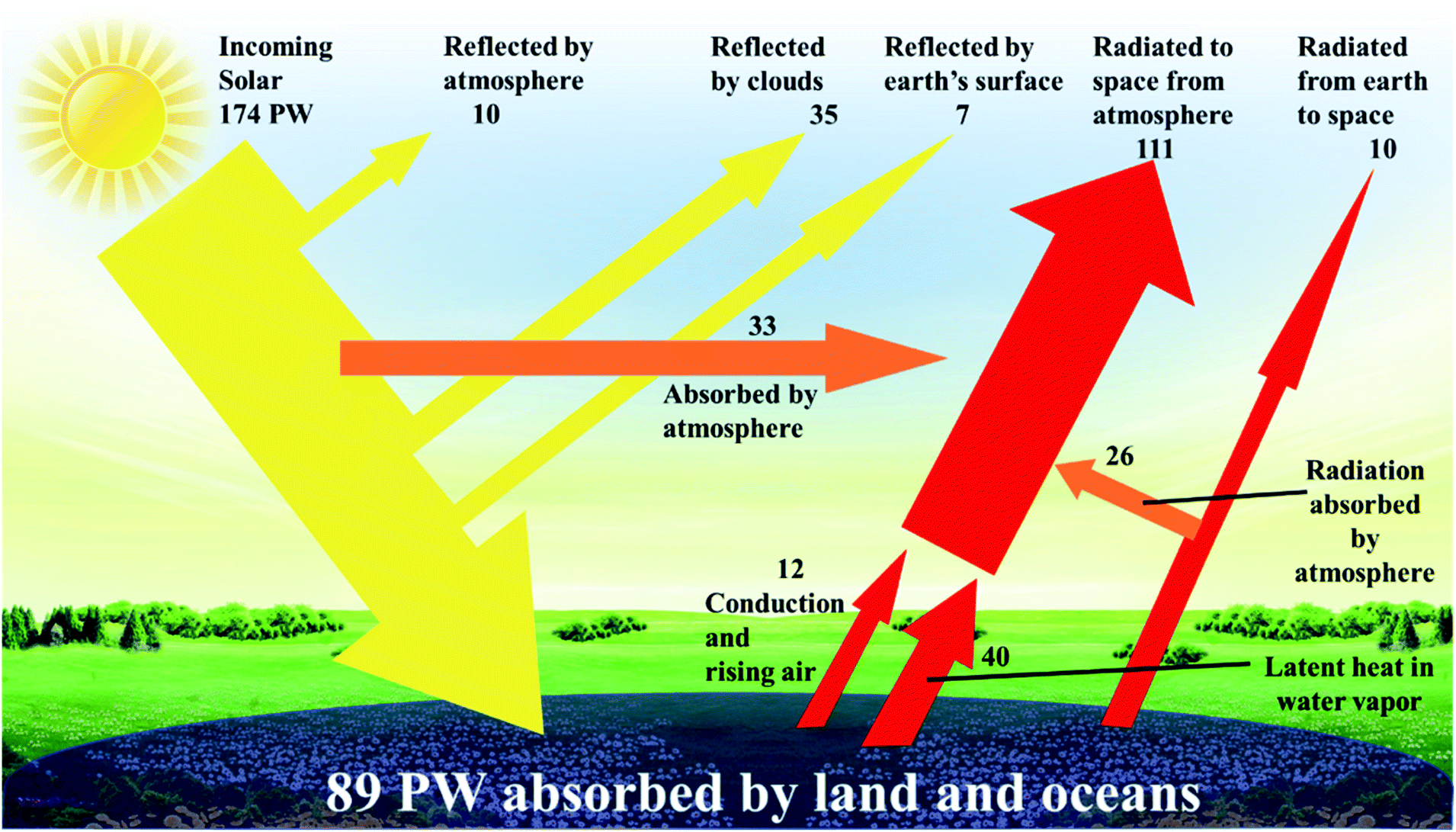 | ||
| Fig. 1 Incoming solar power distribution is reflected and absorbed in many ways.5 | ||
The photovoltaic (PV) effect describes the generation of an electric current and voltage in a material incident with radiation (predominately light) and is a physical and chemical phenomenon. The PV effect was first observed by French physicist, A.E. Becquerel, in 1839 while studying liquid electrolytes.6 From the 1950s, this effect has been studied with a wide range of materials and different device architectures ever since the discovery of Chapin that a silicon-based, single p–n junction device with a solar power conversion efficiency (PCE) of approximately 6% was achieved in 1954.7 PV technology is currently dominated by wafer-sized single junction solar cells based on crystalline silicon that are assembled into large area modules. These first-generation solar cells have dominated the PV market due to their relative low-cost and large-scale manufacturing capability.8,9
Today, the most successful crystalline silicon solar cell has been the passivated emitter and rear cell (PERC),10 pioneered by M.A. Green and his team since the 1980s.11 However, due to the limitations of single-junction crystalline silicon solar cells, including finite photon conversion and rigid nature, several alternatives have been proposed such as thin film devices based on cadmium telluride, copper indium gallium selenide, and amorphous silicon. Thin-film technologies, which require less materials to form devices, are known as second generation PV solar cells. Even though these second-generation devices can be less expensive with respect to materials, production costs can be higher, and they are still lower in overall light to electrical PCE than their first-generation counterparts. Simultaneously, organic semiconducting materials have advanced very rapidly to provide a range of organic-based devices, such as organic PV cells, since Tang reported a single heterojunction organic PV cell with PCE of 0.95%.12 This work represented a major milestone for the development of organic-based semiconductor PV devices. From the late '80s to early '90s, high-purity conjugated polymers paved the way for the fabrication of organic PV devices and these cells – addressing further cost reductions through lower materials costs based on organic materials and processing techniques – are referred to as third-generation PV technologies.13–16 In addition to organic heterojunction PV devices, third generation technologies include a variety of other devices, including dye sensitized solar cells (DSSCs),17 perovskite solar cells (PSCs),18 and advanced technologies such as tandem and multijunction solar cells which allow the solar cell efficiency to surpass those of its single-junction counterparts.19–21 Tandem and multijunction solar cells may consist of a single device technology or mixture of technologies from different generations, for example GaInP/GaInAs/Ge, a-Si/nc-Si/nc-Si (thin film), perovskite/silicon, perovskite/CIGS, perovskite/perovskite and more.22 These third-generation devices are a promising cost-effective alternative to the conventional first-generation silicon-based solar cells as their main advantages include: ease of processing (solution processability), mechanical flexibility and versatility of chemical structures and properties from advances in organic chemistry.23–26 However, their commercial viability and production is a considerable challenge for research and industry as they exhibit moderate efficiencies, lower stability and, in some cases, higher cost compared to conventional silicon-based solar cells. There are extensive efforts to solve these issues with the development of organic PV devices, in fact, the widespread commercialisation of PSCs is anticipated in the near future.
Though PV devices can be classified by their fabrication strategies and chronological development over time, a more appealing approach would be to classify PV technology by the nature of their active, or light absorbing material as shown in Fig. 2.27,28 Here, active materials form three major classes: silicon-based, inorganic semiconductors, and emerging or novel materials which contain amongst other materials, perovskite.
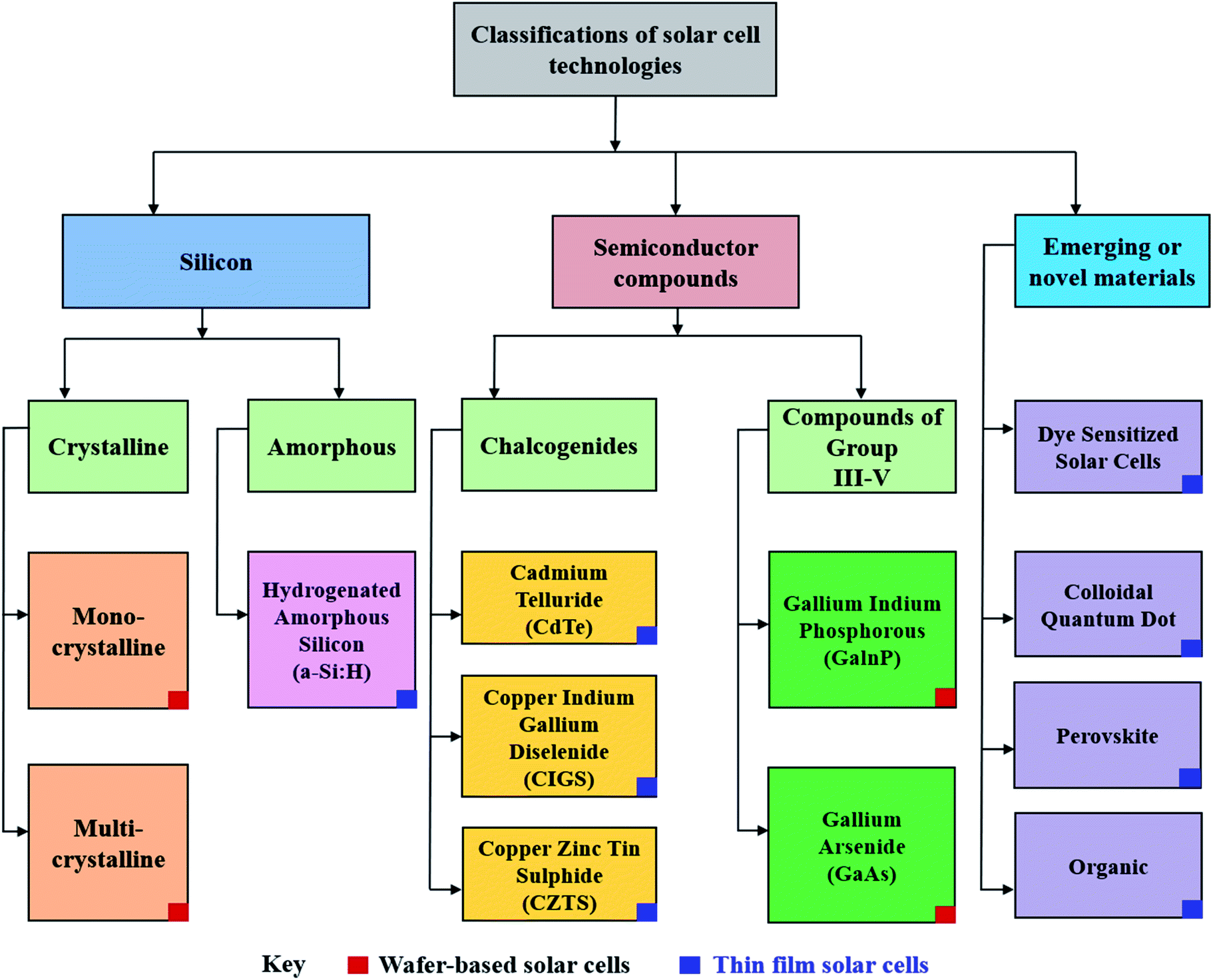 | ||
| Fig. 2 Alternative classification of solar cells based on the primary light-absorbing material within the device.27 | ||
The simple architecture of a typical PSC device contains three major components. The first comprises an absorbing layer which is an organic–inorganic hybrid halide-based perovskite material of general formula ABX3, where A and B are cations of various sizes (typically A = CH3NH3+, CH(NH2)2+ or Cs+ and B = Pb2+ or Sn2+) and X is a monovalent anion, typically the halide anions, I−, Br−, Cl−, and a combination thereof.
The general macromolecular structure is shown in Fig. 3. The second component of a PSC device is the charge-carrying transport layers, which include electron and hole transporting layers that are responsible for extracting and transporting electrons and holes, respectively, from the perovskite layer to the corresponding electrodes. The third component is the electrodes, which comprises of an anode and a cathode. A variety of electrodes, including indium tin oxide (ITO), fluorine tin oxide (FTO), gold (Au), silver (Ag), copper (Cu) and aluminium (Al), have been frequently reported in the literature.29 Using these key three components, the most commonly assembled structures for PSC device architectures can be classed as: (1) mesoporous n–i–p (note: the letters n, i, and p stand for n-type layer, perovskite/light-absorbing layer (intrinsic), and p-type layer in a perovskite device geometry), (2) planar n–i–p, and (3) inverted p–i–n, as depicted in Fig. 4.
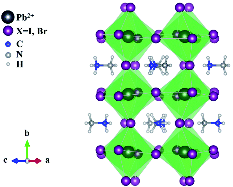 | ||
| Fig. 3 Structure of a typical perovskite ABX3 crystal structure where A and B are cations of different sizes, e.g. CH3NH3+ and Pb2+, and X is a monovalent anion, e.g. I− or Cl− or Br−. | ||
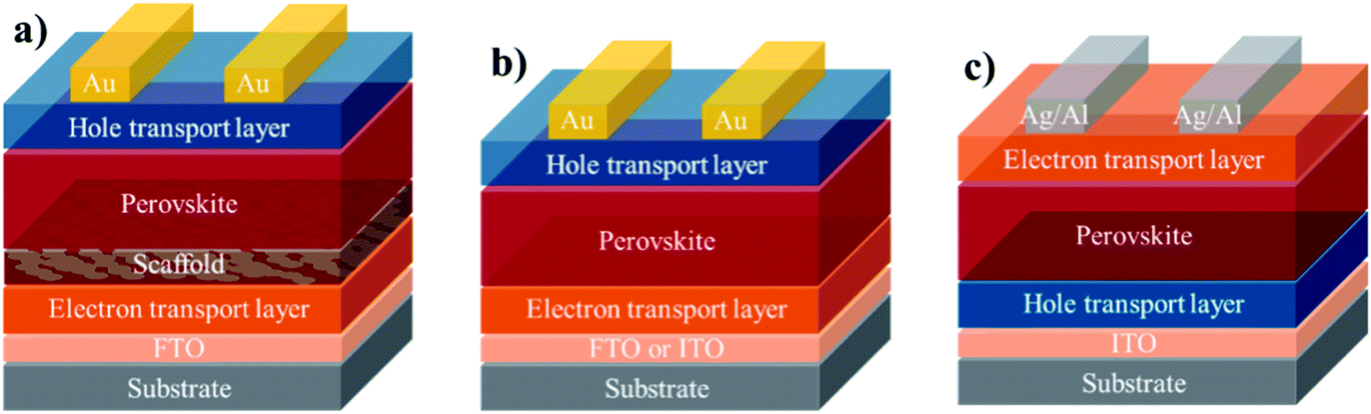 | ||
| Fig. 4 Examples of commonly used PSC device architectures, (a) mesoporous n–i–p, (b) planar n–i–p, and (c) inverted p–i–n [note: the letters n, i, and p stand for n-type layer, perovskite/light-absorbing layer (intrinsic), and p-type layer in a typical perovskite device geometry]. | ||
The earliest reports for PSCs reported the use of methylammonium lead iodide and methylammonium lead bromide as the light absorbing materials.30 The reported PCE of these as DSSCs was low at 3.8%, yet the use of such organic–inorganic halide materials instigated a new research theme which was explored in terms of new material design and creative device fabrication strategies. In 2011, Park and co-workers reported an increased PCE of 6.5% for MAPbI3-based devices where they modified both the titania surface and the processing method of depositing the perovskite layer.31 In 2012, this idea was advanced further through the seminal reports on solid-state PSCs published by the Snaith and Grätzel groups, which used mixed-halide compositions of the photoactive materials (MAPbI3 and MAPbI3−xClx) deposited onto a mesoporous TiO2 layer.32 In that same year, the Snaith group also reported on a hybrid PSC based on a meso-superstructured organometal halide perovskite. The highly crystalline perovskite absorber, with intense absorptivity of 350 nm to ∼950 nm, was fabricated in solution-processed PSC devices and afforded a PCE of 10.9%.33 Since then, research on PSCs has intensified with the most recent reports of PCE of >25% challenging the status of silicon as the dominant semiconductor material for low-cost photovoltaics.34,35 Importantly, stability of the highest efficiency devices (>24% PCE) in humid conditions without encapsulation has improved significantly over time.36 It is evident that given the efficiency/fabrication cost ratio of PSCs, this technology is considered more viable for global future energy needs when compared with other third-generation technologies such as OPVs and DSSCs.
2. Organic electron transport layer materials
The ETL (sometimes called the electron extraction layer or electron collection layer) is a layer in a given PSC device architecture where the electrons are injected from the absorber layer, transported through this layer, i.e. through the thin film of an ETL material, and finally collected by the electrode. For this to occur efficiently, the energy levels, i.e. the highest occupied molecular orbital (HOMO) (or valence band maximum) and the lowest unoccupied molecular orbital (LUMO) (conduction band minimum), of an ETL material and the perovskite layer should complement each other. Having said that, the ETL material should also have the LUMO and the HOMO levels higher than the perovskite active layer. The ETL material should, ideally, have high transmittance in the UV-Vis region, depending upon the type of device architecture, so that photons can pass through and be absorbed by the perovskite layer. It is evident from the current literature that inorganic metal oxides, such as TiO2, SnO2, ZnO (Fig. 5), are usually preferred as ETL materials, with each material having specific advantages to boost the PCE.37–39 Among the reported metal oxides, TiO2 is an ETL material that has been most widely used by various research groups. However, Leijtens et al. reported lower stability of PSC devices with the use of TiO2 (due to its high photocatalytic activity under UV light) as an ETL material when compared with a TiO2-free PSC.40 Apart from the stability issue, another drawback of using TiO2 as an ETL material is that the film has to be annealed at a higher temperature, which not only can be a great barrier in the commercialization of PSC technology but is incompatible with the use of flexible substrates that may not bear such high temperatures. While the use of mesoporous TiO2 can achieve good efficiency, their counterpart, i.e. the planar PSC devices, suffers from hysteresis issues. A number of research groups have replaced TiO2 with SnO2 to achieve efficient, stable, and low-temperature processed PSCs.41 Researchers have also employed atomic layer deposited (ALD) SnO2, but the ALD process42 may not be as commercially feasible or cost-effective. Therefore, it is discernible that the commonly used metal oxides as ETLs have several drawbacks that need to be overcome. One of the strategies is the design and development of organic materials, and research over the past two years has helped to narrow the performance gap between the ETLs based on metal oxides and organic materials, thus, yielding a new generation of highly-efficient ETL materials.43,44 The key advantages of using organic materials include lower processing cost and straightforward synthetic protocols, higher solubility, and tunable optoelectronic properties through suitable molecular engineering. The majority of these organic materials feature a series of common design elements, e.g. are donor–acceptor (D–A) systems where an electron donating building block is linked to an electron accepting group through a π-linker. Another promising molecular design is an A–A–A format where a variety of acceptor building blocks can be joined to generate a target chromophore. Such systems are highly flexible and can be tuned according to the requirements of film transparency, solubility and chemical stability. Moreover, small variations within these different sections, i.e. in D and A, cause significant difference in photovoltaic performance. Recent literature suggests that the use and choice of an electron acceptor functionality plays a vital role in designing new targets – either small molecule or polymer based – as the developed target should possess desirable properties such as high electron mobility and excellent accepting strength.45–47 Therefore, it is important to extend research into organic materials to evaluate design strategies capable of building upon the merits described above. As depicted in Fig. 4, every PSC architecture uses selective interlayer materials, namely ETLs and hole transport layers (HTLs) which help to extract charges and improve PSC performance. A variety of inorganic and organic materials have been reported. For example, the most commonly used HTLs used in PSCs are Spiro-OMeTAD,48 PTAA,49 PEDOT:PSS50 and nickel oxide (NiO).51 Similarly, a variety of materials have been used as ETLs, including metal halides and oxides,52–55 organic small molecules,56 conjugated polymers,57 and non-conjugated polymers.58 These layers are often sandwiched between the electrodes and the perovskite layer, and their main function is to facilitate efficient charge extraction while reducing carrier recombination. Fig. 5 illustrates commonly used charge-extraction layers.59 Some argue that organic small molecules are particularly attractive for use as ETLs as they: (1) possess well-defined chemical structures, (2) are easy to synthesize through simple and straightforward synthetic strategies, (3) hold monodisperse molecular weight, and (4) can be purified using convenient purification methods such as through simple column chromatography.60–62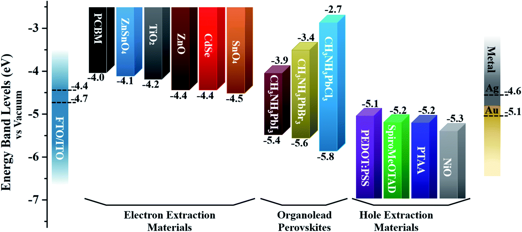 | ||
| Fig. 5 The band energy level diagram for commonly utilized charge-extraction layer materials and CH3NH3PbX3 perovskites. Note: the dotted lines represent the work functions of various electrodes. | ||
To improve the PCE of PSC devices, it is critical to choose the right ETL material whose energy levels complement those of both the electrodes and the light absorbing perovskite layer. A variety of organic HTL materials have been investigated in detail, and a number of reviews on their evolution and performance have been written.63–65 Curiously, even though ETL materials are considered to have a critical effect on the performance of PSCs, the development of organic ETL materials has lagged the development of HTL materials. To design an efficient organic ETL material, various parameters must be considered:
(1) The material should be highly soluble in an orthogonal solvent – a solvent that is different than the solvent of perovskite film fabrication – because the PSC device is a multilayer structure.
(2) The ETL material should possess good electron mobility and a common way to achieve this is through a conjugated structure. This is vital to improve the ability of electron transport to the cathode and deliver low series resistance.
(3) The film of an ideal ETL should easily coat the surface of the absorbing layer to avoid a direct contact between the electrode and perovskite layer, which could result in current leakage through local shunting.
(4) The energy levels, i.e. the LUMO and the HOMO, of an ETL molecule must complement the conduction and valence bands of the perovskite layer, respectively. Having said that, the LUMO of an ETL material should be lower than the conduction band and the HOMO value should be higher than the valence band of the perovskite layer, respectively. This is to mitigate the open-circuit voltage (Voc) loss and to enhance electron extraction for optimum performance.
(5) An efficient ETL material should have electron rich centres, e.g. units containing heteroatoms such as nitrogen and sulfur. These units can act as Lewis bases and can coordinate with available Pb ions exposed at the surface to effectively passivate defects in the perovskite film. This could help to improve Voc and fill factor, hence, overall device performance.
(6) To complement the requirement of a material's dissolution in several orthogonal solvents, its printability must be considered in order to prevent the damage of the perovskite layer after spinning.
ETL materials can play a crucial role in the design of PSC device architecture and should be thought of as the backbone of this emerging technology. Therefore, the discovery of new materials that not only improve device performance but are based on straightforward synthetic strategies are critical. The beauty of organic-based materials is the structural diversity possible (Fig. 6), which lends itself to broad interpretability and optimisation of points 1–6 above. For example, an ETL material based on planar coronene and fabricated in a conventional n–i–p PSC architecture reported a high efficiency of >17% on a rigid and 14.2% on flexible devices.66 The fullerenes, di(3-(pyridin-4-yl)propyl)[60]fullerenyl malonate (PCP) and di(1-methoxyethyl)[60]fullerenyl malonate (MCM), possess almost identical optoelectronic properties as ETL materials, affording efficiencies beyond 19% with a planar absorber layer over 1 micrometre, yet display different passivation strength influence on the hysteresis of the device through the change in terminal group.67 The two ETL materials, 3-[6-(diphenylphosphinyl)-2-naphthalenyl]-1,10-phenanthroline (Phen-NaDPO) and its blend with tin(II) thiocyanate, i.e. Phen-NaDPO:Sn(SCN)2, exhibited an improvement in the PCE from 16.6% to 18.2% in an inverted device configuration ((p–i–n); ITO/NiO/CH3NH3PbI3/PC60BM/ETL/Ag).43 To show the structural diversity even more pronouncedly, thiol-functionalised 2D metal–organic framework built into a stable PSC device recorded a PCE of 22.0% along with substantially improved long-term operational stability.44 Similarly, a multifunctional interfacial layer comprising a non-fullerene electron acceptor, Y6 (Fig. 6), was recently used to replace the conventionally used PC61BM and to enhance the device efficiency together with the operational stability of p–i–n structured devices.68 The presence of various functional groups on Y6, such as fluoro, cyano and sulfur, helped to increase the efficiency of electron transport, suppress ion migration to improve device performance, trap passivation, and enhance near-infrared photocurrent. Though the device geometry constructed was complex, a PCE of 21.0% was achieved, with enhanced operational stability (up to 1700 h) upon exposure to light, heat, and moisture. Another example of a promising non-fullerene acceptor that has been used as an electron transport material is COi8DFIC (Fig. 6), which when combined with the perovskite, MAPbBr3, leads to high-performance, visible/NIR dual-colour photodetector with a structure of ITO/PTAA/MAPbBr3/COi8DFIC/Ag.69 The new acceptor is an A–D–A type non-fullerene acceptor with an electron-rich carbon–oxygen-bridged core unit and two electron-deficient terminal units. The acceptor affords high charge carrier mobility, low-energy light-harvesting, and a non-overlapping absorption with MAPbBr3. Even though the perovskite based on the combination of MA and PbI3 is often used, reports of a PSC with CsPbI2Br as a light absorption material and a binary ETL comprising PC61BM and SFX-PDI2 have been reported.70 The newly designed non-fullerene acceptor, SFX-PDI2, based on spiro[fluorene-9,9′-xanthene] and perylene diimide structural units, were used in conjunction with the traditional acceptor, PC61BM, to improve charge extraction, tune morphology. As a result, the binary ETL-based PSC afforded an efficiency of 15.12%, a result that is among the highest efficiency numbers for inverted planar structured all-inorganic PSCs. Given the excellent photoelectron chemical properties and suitable energy level alignment with perovskite, perylene diimide-based ETL materials where the perylene diimide units were attached to a phenothiazine 5,5-dioxide (PDO) core building block to generate a dimer (PDO-PDI2) and a trimer (PDO-PDI3) have been reported.71 When applied in PSCs, the PDO-PDI3-based PSC exhibited an efficiency of 18.72% with no hysteresis and excellent long-term stability.
 | ||
| Fig. 6 Structural diversity in organic ETL materials of both fullerene and non-fullerene types. | ||
3. NDI-based electron transport layer materials
The use of functionalities such as naphthalene diimide (NDI, Fig. 7) in the design of next-generation ETL materials should be anticipated. The inclusion of NDI functionality in a given target is advantageous as not only is it a strong acceptor group and strong chromophore with appropriate physical and electronic properties to be considered for ETL materials, but the functional diversity helps to improve solubility of a given target by allowing substitution at its imide and/or core positions.72–78 The incorporation of a variety of solubilising chains, e.g. lipophilic, hydrophilic, alkoxy, aliphatic with terminal thiol groups, and polyethylene glycol, at imide positions enhances the solubility of a proposed target, a result that is of great significance to generate excellent pristine and blend films of the proposed target material without crystallisation.79–82 Therefore, it is timely to review the literature of ETL materials based on NDI functionality and to correlate the structural features with the device performance in order to determine useful design concepts to advance the area. This review provides the current state-of-the-art in the field of ETL materials, both polymers and small molecules, comprising NDI functionality for PSCs and describes structure–property relationships. We also outline future perspectives from a materials chemistry viewpoint, outlining the correlation between structural aspects and device performance. It is critical to mention here that a number of factors, including environmental factors impacting stability of PSC devices and their toxicity and shorter lifetime, are already discussed in a number of recent review articles,83–90 and the reader is encouraged to consider the respective sections of these reports for articles relevant to these specific areas. This review is written from a perspective of organic chemistry, and we believe this will provide fundamental advice on the future design of new ETL materials based on NDI format that will afford more efficient and stable PSCs.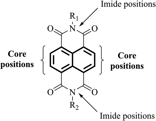 | ||
| Fig. 7 Structure of naphthalene diimide (NDI) core. | ||
The choice of an acceptor functionality is critical to design new ETL materials and that most of the high-performing organic ETL materials are conjugated structures, either through the merger of a variety of building blocks, for instance donor (D) and acceptor (A), or through the possession of a rigid, extended fused-ring backbone, and carry strong acceptor functionalities. Given the challenging structural requirements, for example presence of heteroatoms that can bind to the metal ions of the perovskite layer, and polar groups that can help lower the work function of cathodes, it is apparent that ETL materials based on NDI core should be at the forefront of efficient and logical material design. Briefly, an NDI unit is an electron deficient unit that possesses excellent photo, chemical, and thermal stabilities at room temperature, thus, making is suitable for applications such as light-harvesting, self-assembly, and electronic devices.91,92 A variety of electronic molecules based on NDI core have been prepared into supramolecular arrangements and have influenced the self-assembly of several other organic semiconductors, for example based on cyanopyridone and barbituric acid.93,94 The existence of electron-withdrawing imide fragments within the NDI permits them to be simply reduced chemically or electrochemically into stable anionic radicals while remaining stable to oxidation. Due to the latter, NDI acts as a stable n-type semiconducting core. It is arguable that NDI core offers unique advantages that cannot be considered universal with other functionalities such as fullerene and other non-fullerenes. For instance, the NDI unit is an electron poor unit that accommodates the LUMO density so precisely that it is easy to expand its electronic character using simple synthetic protocols. On the contrary, other non-fullerene acceptor functionalities such as rhodanine, cyanopyridone, and malononitrile do not possess this feature, thus, restricting their use for the development of ETL materials. Moreover, due to its additional properties, such as structural functionalisation at imide and core positions, and excellent light-absorbing in the high-energy region, NDI is known as a promising candidate for generating targets that can be used in applications such as OPVs, OFETs, and OLEDs.95–101 The same can be said for ETL materials for PSC technology.102
NDIs generated through imide nitrogen substitution usually possess similar optoelectronic properties because the electron density nodes in the LUMO and the HOMO levels at imide positions reduce the coupling between the NDI unit and the imide substituents to a minimum. For typical NDIs, this leads to an optical transparency above 340 nm. Having said that, this is an excellent way to functionalise NDI using a variety of connectors and to tune its processability. The targets that are generated using core substitutions are usually highly conjugated materials and depending upon the substitution, several parameters, such as solubility, optical bandgap, crystallinity, thermal and chemical stabilities, and light-harvesting, can be significantly altered. Moreover, such substitutions can assist in minimising the π–π overlap between aggregating naphthalene subunits to improve the performance of the resulting devices by changing the morphology and self-assembly of NDIs. Furthermore, materials based on NDI format can be engineered to address the trade-off between device stability and efficiency. Such materials can be easily synthesized, scaled-up, and compete with champion ETL materials, for example fullerenes and metal oxides, by keeping desirable properties such as high electron mobility, solubility, chemical and thermal stabilities, and excellent accepting strength. Moreover, the use of both small molecule and polymeric approaches exists. Such advantages are likely to be responsible for prompting interest in the design of target ETL materials based on NDI functionality.
3.1 Polymeric electron transport layer materials based on NDI format
One of the first NDI-based ETL materials reported was polymeric.103 Three polymers, namely N2200/(P(NDI2OD-T2), PNVT-8, and P(NDI2OD-TT) (Fig. 8) were based on the conjunction of NDI and thiophene functionalities where the latter was arranged either linearly or in fused form. The incorporation of vinyl linkages into the polymer backbones maintained the LUMO energy levels, thereby facilitating electron injection. Inverted PSC devices were fabricated (device structure: ITO/PEDOT:PSS/CH3NH3PbI3−xClx/ETL/ZnO/Al) and the reported PCEs were 8.15%, 7.47%, and 6.47%, for N2200, PNVT-8 and P(NDI2OD-TT), respectively. The PCE results were competitive to the efficiency achieved using PCBM as the conventional ETL material of 8.51%. For the higher-performing polymer (N2200), the thicknesses of the ETL and perovskite layers were ∼80 nm and 170 nm, respectively. This work demonstrated that conjugated polymeric materials comprising D and A building blocks were efficient ETL materials and worth further exploration. Taking into account this combination and the success of D and A units, further reports emerged, for example an amino-functionalized copolymer, PFN-2TNDI, where the polymeric backbone was composed of fluorene (D unit), naphthalene diimide (A unit), and thiophenes (π-spacers) (Fig. 8).104 The polymer exhibited good electron mobility of 4.8 × 10⁻⁴ cm2 V−1 s−1 and was adequately soluble in a number of solvents to produce useful devices. This research realised that the presence of tertiary amine groups on the polymer side chain can passivate the surface traps of the perovskite layer to improve the electron extraction properties, which is now a growing area of research105 and can reduce the work function of the metal cathode by forming desired interfacial dipoles. The PSCs were fabricated with an inverted device architecture, ITO/PEDOT:PSS/CH3NH3PbI3−xClx/PFN-2TNDI/Ag), and a high PCE of 16.7% was recorded – significantly higher than the efficiency obtained using the conventional ETL material PCBM (12.9%). The optimum thickness of the electron extraction layer was found to be 50–100 nm, which yielded an average PCE over 15%. The devices based on this new polymer were found to be more stable when compared with the devices based on PCBM as the PCE dropped to 50% of its original value after 160 hours of storage time, while it only took 40 hours for PCBM-based devices to see a comparable reduction. The stability of devices was further attributed to the stronger packing between polymer chains, which provided a better physical barrier to reduce the water penetration rate to the perovskite layer – a major degradation source for PSCs.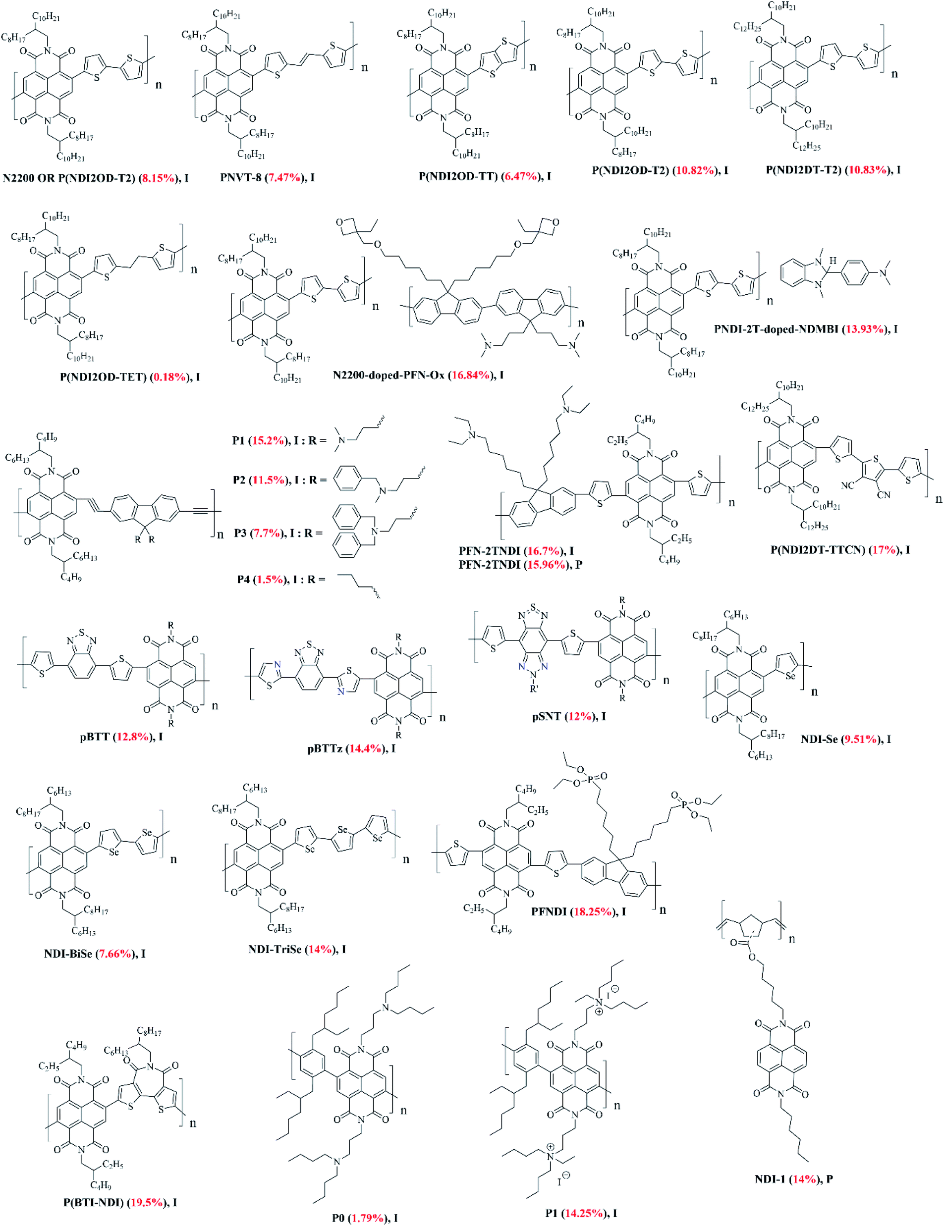 | ||
| Fig. 8 The chemical structures of NDI-based polymers reported in this review article (I and P refer to inverted and planar devices). Optimal PCEs are quoted in brackets for each material. | ||
Given the success of conjugated polymers as efficient ETL materials, new reports on a series of conjugated polymers, P(NDI2OD-T2), P(NDI2DT-T2), and P(NDI2OD-TET) (Fig. 8), comparing the performance of the literature reported P(NDI2OD-T2) polymer with their structural analogues were made.106 The longer side chains in these new polymers helped to enhance solubility, and hence processability, without influencing the energy levels and optical bandgap. The ethylene unit in the backbone of P(NDI2OD-TET) reduced the conjugation length, leading to a wider bandgap. Coating of ETL layers over perovskite film produced a much smoother surface, featuring a surface roughness of ∼4–6 nm. The inverted devices were fabricated (ITO/PEDOT:PSS/CH3NH3PbI3−xClx/ETL/Al) and exhibited PCEs of the order 10.82%, 10.83%, and 0.18% for P(NDI2OD-T2), P(NDI2DT-T2), and P(NDI2OD-TET), respectively. The maximum efficiency of the fabricated devices using the n-type polymers did not exceed the performance of devices based on the conventional PCBM (∼11%), though the authors claimed that the ambient stability of devices was considerably improved with the use of ETL polymers when compared with the device stability based on the latter. Given the success of (P(NDI2OD-T2)), as an efficient, n-type polymeric ETL material, together with its commercial availability, many research groups have now studied this polymer along with its structural analogues and by altering device fabrication conditions. In one such study, the electronic properties of N2200 were modified with a polymeric additive, poly[9,9-bis(6′-(N,N-diethylamino)propyl)-fluorene-alt-9,9-bis(3-ethyl(oxetane-3-ethyloxy)-hexyl) fluorene] (PFN-Ox).107 The inverted devices were fabricated (ITO/NiO/MAPbI3/N2200:PFN-Ox/bis-C60/Ag) and the device performance was enhanced to 16.8% with the use of N2200:PFN-Ox as an electron extraction layer. The use of the conventional PCBM as an ETL material provided 16.62% efficiency, although the device's ambient stability was seen as inferior to that of devices based on N2200:PFN-Ox. This study demonstrated the potential of using polymeric ETLs to replace the commonly used PCBM to enhance the performance and stability of PSCs.
Efficient doping to high-performing polymers leads, in principle, to better ETL materials. For example, when PNDI-2T is doped with (4-(1,3-dimethyl-2,3-dihydro-1H-benzoimidazol-2-yl)phenyl)dimethylamine (N-DMBI)108 in fabricated inverted p–i–n devices (glass/ITO/PEDOT:PSS/perovskite layer/ETL (PNDI-2T/PNDI-2T + N-DMBI)/PEIE/Au), the doping doubled the efficiency from 6.5% to 13.93%. Interestingly, this same study investigated the thickness of the electron extraction layer and found that a 20 nm thick film afforded the best device parameters. The film thickness of 50 nm, 35 nm and 14 nm provided PCEs of the order 3%, 12% and ∼10%, respectively, thus, suggesting the importance of ETL thickness and its correlation with the device performance. Stability experiments indicated that the doped devices were far more stable than the undoped devices, where the former retained 85% of the PCE value after 150 hours and the latter kept 62% of the original value.108 The dopant, N-DMBI, not only increases the conductivity of polymeric ETL, but also lowers the LUMO and the HOMO values, thus, improving both electron extraction and hole blocking abilities. Based on previous work,104 Li et al. reported the polymer PFN-2TNDI as an ETL material and demonstrated a 15.96% efficiency in fabricated planar n–i–p devices (device architecture: ITO/PFN-2TNDI/MAPbI3−xClx/spiro-OMeTAD/Au), at optimized thickness of the ETL at 5 nm – a result which was comparable to that of inorganic TiO2 ETL-based devices (17.20%).109 Moreover, the devices were processed at low temperature and showed enhanced photostability against UV irradiation when compared with the devices based on TiO2, thereby addressing, in part, photostability issues encountered in perovskite devices.
Polymer design can also be varied to achieve enhanced performance. A series of novel, n-type conjugated polymers, coded as P1 to P4, with amino-functionalized side groups were prepared (Fig. 8).110 The copolymers comprised fluorene and NDI units within the identical backbone, but containing different pendants of N,N-dimethylamino, N-methylbenzylamino, N,N-dibenzylamino, and pure alkyl chains. The choice of using NDI in the polymer backbone was based on the premise that it possesses large electron affinity and has been used to construct n-type organic semiconductors with excellent electron mobility for OPVs and OFETs. The amino functionalisation could be used to fine tune the work function of the cathode for better electron extraction and to passivate the surface traps of perovskite for a reduction of charge recombination, given the electron rich nitrogen heteroatom(s). The PSCs were fabricated based on the device configuration of ITO/PEDOT:PSS (∼40 nm)/MAPbI3−xClx (∼400 nm)/ETL (∼50 nm)/Ag, and the photovoltaic performance was studied. Although the authors reported two more polymers, P5 and P6, which were devoid of acetylene spacers, their fabrication into PSC devices was unreported. The PCEs of the PSC devices with P1 to P4 as the ETLs were 15.2%, 11.5%, 7.7%, and 1.5%, respectively. For the highest performing polymer P1, devices of various ETL thickness were fabricated. For an optimal thickness of ∼50 nm, the devices based on a P1 interlayer produced a PCE over 15%, however, as the thickness of interlayer increased past this, the PCE decreased. It was evident from this work that a number of structural elements are essential to create efficient ETL materials based on the NDI core. Structural features, such as (1) extended conjugation between NDI and donor units, (2) use of π-spacers, e.g. an acetylene unit, in a given molecular backbone, (3) inclusion of amino-functionalised groups, are critical and can help to generate an ETL target material with enhanced electron-transporting property. Moreover, with the inclusion of such structural features it is viable to develop novel thickness-insensitive ETL materials, and this in many respects is proportional to electron mobility. Kim et al. reported the polymer (P(NDI2DT-TTCN)) composed of NDI and donor oligothiophenes with one of the thiophenes bearing electron-withdrawing dicyano functionalities as an ETL material (Fig. 8).111 Within inverted p–i–n devices (device architecture: glass/ITO/HTL/CH3NH3PbI3/ETL/metal) with P(NDI2DT-TTCN) and PCBM as electron extraction layers, the performance of devices based on P(NDI2DT-TTCN) significantly outperformed the devices based on PCBM alone (17.0 vs. 14.3%). The enhanced performance was attributed to the polymer's ability to improve the electron extraction together with the long-term stability of PSC devices under ambient conditions. The P(NDI2DT-TTCN)-based electron-only device showed a higher electron mobility (μe = 7.71 × 10⁻⁴ cm2 V−1 s−1) when compared with the device based on PCBM (2.53 × 10⁻⁴ cm2 V−1 s−1), suggesting that P(NDI2DT-TTCN) could promote a better vertical charge transfer than PCBM for the inverted PSC devices. This report provided some valuable design guidelines for originating new polymeric ETL materials for high performances in flexible PSCs.
Three conjugated polymers, pBTT, pBTTz, and pSNT, based on the donor–acceptor1–donor–acceptor2 (D–A1–D–A2) format were designed and synthesised as ETL materials for PSCs (Fig. 8).112 In addition, the effect of substitution position of sp2-N atoms on the PSC performance was investigated. From a structural perspective, the investigated polymers are NDI-based, n-type polymers, with field-effect electron mobilities up to 0.92, 0.46, and 4.87 cm2 V−1 s−1, respectively. Since they demonstrated good performance in organic and tandem solar cells, the authors of this research surmised they should perform well in PSC devices. The fabrication of pBTT, pBTTz, and pSNT as ETLs in inverted PSC devices (ITO/PEDOT:PSS/CH3NH3PbI3−xClx/ETLs/Ag) afforded PCEs of the order of 12.8%, 14.4%, and 12.0%, respectively. Though the introduction of sp2-N atoms into the donor thiophene units of pBTT (producing pBTTz) exhibited a slightly lower electron mobility [μe (pBTT) = 0.92 cm2 V−1 s−1; μe (pBTTz) = 0.46 cm2 V−1 s−1], the PCE of PSCs were still significantly improved. On the contrary, pSNT with two additional sp2-N atoms and very high electron mobility [μe (pSNT) = 4.87 cm2 V−1 s−1] showed only moderate PSC performance. The electron-rich sulfur atoms (in donor thiophene units) appear to have a strong impact on the passivation of under-coordinated Pb-atoms, as reflected by the current density–voltage hysteresis curves of the pBTTz-based devices. Given the presence of electron-rich heteroatoms and NDI functionality, the polymers were hydrophobic in nature and were thus able to retain device stability over a substantial amount of time, e.g. the pBTTz-based devices retained 80% of its stability after ten days. This study was the first demonstration where the effect of sp2-N position in the main polymer chain, i.e. in the backbone of the parent polymer pBTT, on the photovoltaic properties of PSCs was investigated.
It is evident that the combination of NDI with donor functionalities, and thiophene in particular, produced polymer backbones that were rich in conjugation, offered excellent electron mobilities, exhibited adequate solubility in a variety of solvents, and were used as efficient ETL materials. In moving from sulfur to selenium, Yan produced three semiconducting polymers, NDI-Se, NDI-BiSe, and NDI-TriSe, via copolymerization with NDI for use as ETL materials (Fig. 8).113 The respective polymers utilized one, two and three selenophene units in conjunction with NDI in the main polymer chains. The three polymers demonstrated excellent thermal stability, high crystallinity, and energy levels complimentary to the perovskite absorber layer. The polymers were fabricated in an inverted device architecture with a configuration of ITO/NiOx/MAPbI2.8Cl0.2/ETL/Ag, and the highest efficiency was achieved with the incorporation of NDI-TriSe (14.0%), an efficiency comparable to the standard cell using thermally deposited C60/BCP bilayer ETL (14.6%). The use of bis- and tris-selenophene units increased polymer planarity and delocalization, and thus conductivity [μe (NDI-TriSe) = 3.0 × 10⁻⁴ cm2 V−1 s−1vs. μe (NDI-BiSe) = 6.0 × 10⁻⁵ cm2 V−1 s−1 and μe (NDI-Se) = 4.3 × 10⁻⁵ cm2 V−1 s−1]. Though the polymer decomposition temperature gradually decreased with the increase in selenophene units, the decomposition temperature of all three polymers was far beyond the frequently used annealing temperature for optoelectronic device applications (100–200 °C). The thickness of the ETL was optimized to be only ∼9 nm, which is considered thin relative to other ETLs used in PSC devices. Deng reported a novel NDI-based conjugated polymer PFNDI by introducing phosphite ester side chains (Fig. 8).114 As a result, PFNDI afforded good solubility in chlorobenzene, a solvent which is compatible with the solution processing of perovskite layers and the generation of smoother films. The introduction of the phosphite ester groups was helpful for the PFNDI to adhere to the perovskite and passivate defects. SEM analysis indicated that the perovskite layer surface was covered by PFNDI layer without any pinholes. From the AFM analysis, it was evident that the perovskite surface was much smoother after it was covered by PFNDI, with the surface root-mean-square roughness reduced from 7.27 nm to 5.09 nm. An inverted device architecture (glass/ITO/HTL/perovskite/PFNDI/C60/BCP/Ag) as PSC devices were prepared with a thickness of ∼5 nm. Devices prepared without PFNDI exhibited a PCE of 17.41%, whereas for the PFNDI-based devices this improved to 18.25%, realizing stable PSCs under atmospheric conditions.
Recently, Y. Shi et al. reported an A–A-based polymer, coded as P(BTI-NDI), based on NDI functionality (Fig. 8).115 The main rational of their design was to replace the conventional PC61BM and to improve the efficiency and stability of PSC devices. The developed polymer exhibited high thermal decomposition temperature of 405 °C and a reasonable electron mobility (4.2 × 10⁻⁴ cm2 V−1 s−1) that was deduced using the space-charge-limited current (SCLC) method. The PSCs were fabricated with an inverted device configuration of ITO/PTAA/perovskite/ETL/BCP/Ag to probe the performance of P(BTI-NDI) and to compare with the conventionally used PC61BM. The P(BTI-NDI)-based device achieved remarkable PCE of 19.5% with negligible hysteresis. Though the efficiency using PC61BM was 20.1%, the authors claimed that the newly designed ETL material showed improved stability compared to PC61BM-based devices. This was primarily attributed to the higher hydrophobicity of the new ETL. They also reported that a thickness of 69 nm was found to be optimal for the higher device outcome.
In other work, S. Valero et al. outlined three novel, NDI-based materials, namely P0, P1 and M1, bearing ternary or quaternary ammonium moieties (Fig. 8).116 The main aim of designing these materials was to use them as buffer layers between fullerene and the metal cathode to improve the performance of PSCs. P1 was an ammonium-bearing NDI polymer, together with its ternary amine polymer counterpart, P0, and its small molecule analogue, M1 (note: for structures of P0 and P1, see Fig. 8 and for M1, see Fig. 9). All materials were found to be thermally stable as their thermal behaviour was investigated by means of thermogravimetric analysis (TGA) and differential scanning calorimetry (DSC) analyses. The newly developed materials demonstrated suitable energy levels with low-lying LUMOs around 4 eV and the HOMOs around 6 eV. They were soluble in polar solvents, thus, allowing the authors to use them as buffer layers, with no risk of dissolving the underlying PC61BM layer during deposition. The chosen architecture of the devices was simple and inverted: FTO glass/NiOx/CH3NH3PbI3/PC61BM/buffer layer/Au. They compared the new materials as buffer layers against the conventionally used buffer layer, bathocuproine (BCP), for PC61BM-based devices. Devices were also fabricated with no buffer layer so that PC61BM directly contacts with the gold cathode. The device performances with polymer P1 and small molecule M1 were highly comparable to those obtained with the reference BCP buffer layer. BCP gave an average 11.82% PCE and both M1 and P1 gave average values of 11.42% and 11.43%, respectively. Without any buffer layer, an average value of 3.48% was reported. It was established from this study that the halogen ammonium salts carry a great potential to improve the performance of perovskite devices and that NDI-based materials are very promising candidates to improve the performance and stability of PSCs.
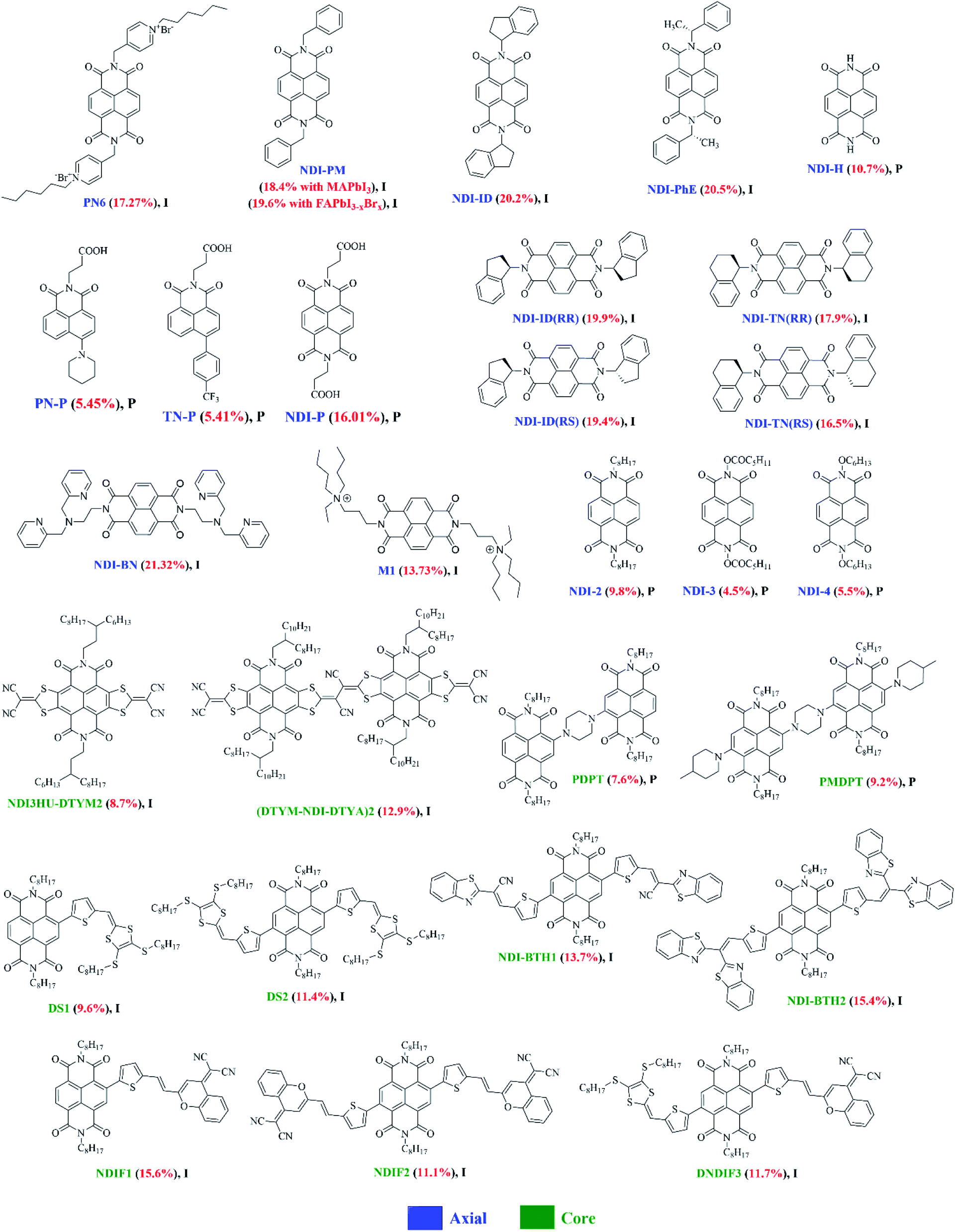 | ||
| Fig. 9 The chemical structures of NDI-based small molecules reported in this review article (I and P refer to inverted and planar devices). Optimal PCEs are quoted in brackets for each material. | ||
A very recent report by K. A. Kurdi et al. mentions a number of NDI-based materials where a new side-chain polymer, NDI-1, is tested against other NDI small molecules as well as SnO2 as a reference (note: the structure of NDI-1 is given in Fig. 8 and of NDI-2, NDI-3 and NDI-4 in Fig. 9).117 This new side-chain polymer exhibited: (1) good transparency throughout the visible region, (2) adequate solubility in low- to medium-polarity organic solvents, (3) resistance to dipolar aprotic solvents such as dimethylformamide, and (4) an appropriate electron affinity for use as an electron extraction layer in lead-halide PSCs. It was established by TGA and DSC that the new side-chain polymer, NDI-1, is thermally stable, with decomposition temperatures above 250 °C, together with other small molecule NDIs, indicating the compatibility with temperatures needed for subsequent deposition and annealing of many hybrid perovskites used in PSCs. The regular n–i–p perovskite devices were fabricated and the performance of NDI-1 was compared to that of several small-molecule NDI derivatives and of SnO2. The best performing device using NDI-1 afforded 14.0% efficiency which was slightly lower than the efficiency achieved using SnO2 (15.6%). Though the efficiency using NDI-1 was lower, it was claimed that the devices comprising the polymer exhibited greater stability than SnO2-based control devices when aged under the one sun conditions for almost 300 hours at 60 °C. This study provided a foundation for designing new NDI derivatives that could be used as dopant-free, solution-processable ETL materials and could potentially replace the conventionally used, metal oxide ETLs such as SnO2.
The photovoltaic performance parameters for each of the polymer systems mentioned in this section are also tabulated in Table 1 to be used as a comparable guide.
| Polymer NDI-based ETL materials | Device architecture | J sc [mA cm−2] | V oc [V] | FF [%] | PCE [%] | Mobility [cm2 V−1 s−1] | LUMO [eV] | HOMO [eV] | Ref. |
|---|---|---|---|---|---|---|---|---|---|
| N2200/P(NDI2OD-T2) | ITO/PEDOT:PSS/CH3NH3PbI3−xClx/N2200/ZnO/Al | 14.70 | 0.84 | 66 | 8.15 | — | −3.93 | −5.66 | 103 |
| PNVT-8 | ITO/PEDOT:PSS/CH3NH3PbI3−xClx/PNVT-8/ZnO/Al | 13.53 | 0.85 | 62 | 7.47 | — | −3.91 | −5.60 | 103 |
| PNDI2OD-TT | ITO/PEDOT:PSS/CH3NH3PbI3−xClx/PNDI2OD-TT/ZnO/Al | 13.71 | 0.81 | 55 | 6.47 | — | −3.87 | −5.73 | 103 |
| PFN-2TNDI-inverted | ITO/PEDOT:PSS/CH3NH3PbI3−xClx/PFN-2TNDI/Ag | 21.9 | 0.98 | 78 | 16.7 | 4.8 × 10⁻⁴ | −3.84 | −5.57 | 104 |
| P(NDI2OT-T2) | ITO/PEDOT:PSS/CH3NH3PbI3−xClx/P(NDI2OT-T2)/Al | 16.90 | 0.884 | 73 | 10.82 | 2.3 × 10⁻⁴ | −4.02 | −5.51 | 106 |
| P(NDI2DT-T2) | ITO/PEDOT:PSS/CH3NH3PbI3−xClx/P(NDI2DT-T2)/Al | 17.10 | 0.899 | 71 | 10.83 | 1.2 × 10⁻⁵ | −4.01 | −5.50 | 106 |
| P(NDI2OD-TET) | ITO/PEDOT:PSS/CH3NH3PbI3−xClx/P(NDI2OD-TET)/Al | 1.41 | 0.715 | 17.5 | 0.18 | 1 × 10⁻⁸ | −3.9 | −5.9 | 106 |
| N2200-doped-PFN-Ox | ITO/NiO/MAPbI3/N2200:PFN-Ox/bis-C60/Ag | 20.5 | 1.09 | 75.4 | 16.84 | — | −3.92 | −5.69 | 107 |
| PNDI-2T-doped-NDMBI | ITO/PEDOT:PSS/perovskite/PNDI-2T-NDMBI/PEIE/Au | 19.8 | — | — | 13.93 | — | −4.40 | −5.85 | 108 |
| PFN-2TNDI-planar | ITO/PFN-2TNDI/MAPbI3−xClx/spiro-OMeTAD/Au | 22.01 | 0.98 | 74 | 15.96 | — | −3.84 | −5.57 | 109 |
| P1 | ITO/PEDOT:PSS/MAPbI3−xClx/P1/Ag | 21.5 | 0.94 | 75 | 15.2 | 2.98 × 10⁻⁴ | −3.92 | −5.96 | 110 |
| P2 | ITO/PEDOT:PSS/MAPbI3−xClx/P2/Ag | 20.6 | 0.94 | 60 | 11.5 | 7.1 × 10⁻⁵ | −3.94 | −5.93 | 110 |
| P3 | ITO/PEDOT:PSS/MAPbI3−xClx/P3/Ag | 19.5 | 0.92 | 45 | 7.7 | 2.5 × 10⁻⁵ | −3.93 | −5.90 | 110 |
| P4 | ITO/PEDOT:PSS/MAPbI3−xClx/P4/Ag | 6.9 | 0.86 | 28 | 1.5 | 9.8 × 10⁻⁵ | −3.97 | −5.98 | 110 |
| P(NDI2DT-TTCN) | ITO/HTL/CH3NH3PbI3/P(NDI2DT-TTCN)/metal | 22.0 | 1.00 | 77.4 | 17.0 | 7.71 × 10⁻⁴ | −4.14 | — | 111 |
| pBTT | ITO/PEDOT:PSS/CH3NH3PbI3−xClx/pBTT/Ag | 22.51 | 0.88 | 64.4 | 12.8 | 0.92 | −3.78 | −5.77 | 112 |
| pBTTz | ITO/PEDOT:PSS/CH3NH3PbI3−xClx/pBTTz/Ag | 21.95 | 0.91 | 72.3 | 14.4 | 0.46 | −3.86 | −6.01 | 112 |
| pSNT | ITO/PEDOT:PSS/CH3NH3PbI3−xClx/pSNT/Ag | 20.5 | 0.88 | 66.5 | 12 | 4.87 | −3.88 | −5.45 | 112 |
| NDI-Se | ITO/NiOx/MAPbI2.8Cl0.2/NDI-Se/Ag | 19.5 | 0.85 | 54.0 | 9.51 | 4.3 × 10⁻⁵ | −6.20 | −4.50 | 113 |
| NDI-BiSe | ITO/NiOx/MAPbI2.8Cl0.2/NDI-BiSe/Ag | 17.7 | 0.86 | 46.4 | 7.66 | 6.0 × 10⁻⁵ | −5.80 | −4.40 | 113 |
| NDI-TriSe | ITO/NiOx/MAPbI2.8Cl0.2/NDI-TriSe/Ag | 20.2 | 0.92 | 62.8 | 14.0 | 3.0 × 10⁻⁴ | −5.70 | −4.50 | 113 |
| PFNDI | ITO/HTL/perovskite/PFNDI/C60/BCP/Ag | 22.53 | 1.068 | 75.85 | 18.25 | 2.07 × 10⁻⁴ | −5.60 | −4.00 | 114 |
| P(BTI-NDI) | ITO/PTAA/perovskite/P(BTI-NDI)/BCP/Ag | 22.7 | 1.10 | 78.5 | 19.5 | 4.2 × 10⁻⁴ | −5.97 | −4.09 | 115 |
| P0 | FTO glass/NiOx/CH3NH3PbI3/PC61BM/P0/Au | 9.5 | 0.56 | 33 | 1.79 | — | −5.94 | −3.53 | 116 |
| P1 | FTO glass/NiOx/CH3NH3PbI3/PC61BM/P1/Au | 21.4 | 1.02 | 65 | 14.25 | — | −6.10 | −3.75 | 116 |
| NDI-1 | FTO glass/NDI-1/perovskite/spiro-OMeTAD/Au | 21.5 | 1.02 | 65 | 14 | — | — | — | 117 |
3.2 Small molecule electron transport layer materials based on an NDI format
It is evident that highly conjugated polymers based on the NDI format have received significant attention as efficient ETL materials in the field of PSCs, and rightly so, achieving impressive efficiencies for organic materials of over 18%. Although an encouraging outcome, there are a reported number of disadvantages associated with their use such as ability to purify, batch-to-batch variations in terms of molecular weight and purity, their lower versatility for deposition processes, e.g., they cannot be deposited via thermal evaporation, and end group deviation. These are all critical considerations and can compromise the overall device outcome. In contrast, small molecules overcome many of these disadvantages, on top of straightforward synthetic protocols and structural modifications to tune the optical bandgap. As a result, small molecules have recently made significant inroads into the PSC research area. Importantly, we demonstrate the flexibility that small molecules based on NDI can be designed by substitutions at either imide nitrogen atoms (axial position) or core positions (Fig. 7). The current literature suggests that both categories can produce efficient ETL materials for PSCs (vide infra). These are summarised in Table 2.| Small molecule NDI-based ETL materials | Device architecture | J sc [mA cm−2] | V oc [V] | FF [%] | PCE [%] | Mobility [cm2 V−1 s−1] | LUMO [eV] | HOMO [eV] | Ref. |
|---|---|---|---|---|---|---|---|---|---|
| PN6 | ITO/NiOx/perovskite/PC61BM/PN6/Ag | 20.53 | 1.11 | 76.07 | 17.27 | 7.1 × 10⁻⁵ | −4.07 | −7.02 | 118 |
| NDI-PM/MAPbI3 | ITO/PEDOT:PSS/MAPbI3/NDI-PM/Al | 21.1 | 1.1 | 79.1 | 18.4 | 1.7/0.72 | — | — | 119 |
| NDI-PM/FAPbI3−xBrx | ITO/PEDOT:PSS/FAPbI3−xBrx/NDI-PM/Al | 22.8 | 1.08 | 79.6 | 19.6 | 1.7/0.72 | — | — | 119 |
| NDI-ID | ITO/PEDOT:PSS/FAPbI3−xBrx/NDI-ID/Al | 23.0 | 1.1 | 80 | 20.2 | 1.5 × 10⁻⁵ | — | — | 120 |
| NDI-PhE | ITO/PEDOT:PSS/FAPbI3−xBrx/NDI-PhE/Al | 23.1 | 1.1 | 80.8 | 20.5 | 1.5 × 10⁻⁵ | — | — | 121 |
| NDI-H | ITO/PEIE/NDI-H/MAPbI3/spiro-OMeTAD/Au | 18.9 | 0.88 | 64 | 10.7 | 5.1 × 10⁻⁵ | −4.0 | −6.9 | 122 |
| PN-P | ITO/PN-P/MAPbI3/spiro-OMeTAD/Au | 10.23 | 0.76 | 69.69 | 5.45 | — | −3.01 | −5.59 | 123 |
| TN-P | ITO/TN-P/MAPbI3/spiro-OMeTAD/Au | 10.93 | 0.94 | 52.94 | 5.41 | — | −3.14 | 6.37 | 123 |
| NDI-P | ITO/NDI-P/MAPbI3/spiro-OMeTAD/Au | 20.57 | 1.05 | 73.98 | 16.01 | — | −3.83 | 6.96 | 123 |
| NDI-ID (RR) | ITO/PEDOT:PSS/(FAPbI3)x(MAPbBr3)1−x/NDI-ID (RR)/Al | 22.9 | 1.1 | 79.1 | 19.9 | 3.5 × 10⁻⁴ | — | — | 125 |
| NDI-ID (RS) | ITO/PEDOT:PSS/(FAPbI3)x(MAPbBr3)1−x/NDI-ID (RS)/Al | 22.7 | 1.09 | 78.4 | 19.4 | 5.5 × 10⁻⁵ | — | — | 125 |
| NDI-TN (RR) | ITO/PEDOT:PSS/(FAPbI3)x(MAPbBr3)1−x/NDI-TN (RR)/Al | 21.9 | 1.06 | 77 | 17.9 | 4.4 × 10⁻⁶ | — | — | 125 |
| NDI-TN (RS) | ITO/PEDOT:PSS/(FAPbI3)x(MAPbBr3)1−x/NDI-TN (RS)/Al | 21.5 | 1.05 | 73.1 | 16.5 | 8.6 × 10⁻⁶ | — | — | 125 |
| NDI3HU-DTYM2 | ITO/PEDOT:PSS/MAPbI3/NDI3HU-DTYM2/Ag | 18.56 | 0.96 | 48.85 | 8.7 | 7.50 × 10⁻⁴ | −4.38 | −6.38 | 127 |
| (DTYM-NDI-DTYA)2 | ITO/PEDOT:PSS/MAPbI3/(DTYM-NDI-DTYA)2/Ag | 22.80 | 0.9 | 62.86 | 12.9 | 6.26 × 10⁻³ | −4.25 | −5.65 | 127 |
| PDPT | ITO/PEDOT:PSS/CH3NH3PbI3−xClx/PDPT/Ag | 22.9 | 0.76 | 44 | 7.6 | — | −3.73 | −5.65 | 128 |
| PMDPT | ITO/PEDOT:PSS/CH3NH3PbI3−xClx/PMDPT/Ag | 22.4 | 0.84 | 49 | 9.2 | — | −3.65 | −5.48 | 128 |
| DS1 | ITO/PEDOT:PSS/CH3NH3PbI3−xClx/DS1/Ag | 23.41 | 0.74 | 55.4 | 9.6 | — | −4.2 | −5.41 | 129 |
| DS2 | ITO/PEDOT:PSS/CH3NH3PbI3−xClx/DS2/Ag | 22.65 | 0.8 | 63 | 11.4 | — | −4.19 | −5.34 | 129 |
| NDI-BTH1 | ITO/PEDOT:PSS/FAyMA1−yPbI3−xClx/NDI-BTH1/Ag | 21.3 | 0.96 | 67 | 13.7 | 14 × 10−5 | −4.32 | −5.97 | 130 |
| NDI-BTH2 | ITO/PEDOT:PSS/FAyMA1−yPbI3−xClx/NDI-BTH2/Ag | 22.13 | 0.98 | 71 | 15.4 | 8.64 × 10⁻⁴ | −4.24 | −5.78 | 130 |
| NDIF1 | ITO/PEDOT:PSS/perovskite/NDIF1/Ag | 23.66 | 97 | 64 | 15.6 | 5.91 × 10⁻⁶ | −3.8 | −5.68 | 131 |
| NDIF2 | ITO/PEDOT:PSS/perovskite/NDIF2/Ag | 18.91 | 80 | 68.8 | 11.1 | 1.53 × 10⁻⁵ | −3.9 | −5.60 | 131 |
| NDIF3 | ITO/PEDOT:PSS/perovskite/NDIF3/Ag | 22.11 | 91 | 56 | 11.7 | — | −3.8 | −5.00 | 131 |
| NDI-BN | ITO/PTAA/perovskite/PC61BM/NDI-BN/Ag | 23.61 | 1.13 | 79.93 | 21.32 | 1.0 × 10⁻⁶ | −7.16 | −4.09 | 126 |
| M1 | FTO glass/NiOx/CH3NH3PbI3/PC61BM/M1/Au | 21.8 | 1.04 | 60 | 13.73 | — | −7.00 | −3.86 | 116 |
| NDI-2 | FTO glass/NDI-2/perovskite/spiro-OMeTAD/Au | 18.3 | 0.98 | 56 | 9.8 | — | — | — | 117 |
| NDI-3 | FTO glass/NDI-3/perovskite/spiro-OMeTAD/Au | 11.6 | 0.91 | 43 | 4.5 | — | — | — | 117 |
| NDI-4 | FTO glass/NDI-4/perovskite/spiro-OMeTAD/Au | 14.8 | 0.84 | 46 | 5.5 | — | — | — | 117 |
Considering the success of PN6, a number of different axially-substituted NDIs were soon reported. Heo reported NDI-PM and compared its performance with the conventional PCBM in inverted structured perovskite planar solar cells (Fig. 9).119 From the design perspective, it was understood that the N-substituted NDI-based compounds are cheaply synthesized by a simple imidation reaction from the commercially-available starting materials and have a comparable solubility and electron mobility to the conventional PCBM. NDI-PM exhibited better electron mobilities of 1.7 cm2 V−1 s−1 and 0.72 cm2 V−1 s−1 in thin film transistors based on single crystals and vacuum-deposited films, respectively, than PCBM (∼1 × 10⁻² cm2 V−1 s−1). The best inverted p–i–n devices (device architecture: glass/ITO/PEDOT:PSS/MAPbI3 and FAPbI3−xBrx/NDI-PM/Al) afforded 18.4% and 19.6% efficiencies, respectively, under 1 sun conditions, which were comparable to those of devices with the PCBM as an ETL (18.9% and 20.0%, respectively). A 40 nm thick ETL layer showed the best efficiency under their experimental conditions. The comparable conductivity and charge separation/injection of NDI-PM ETL with the PCBM ETL, validates the strategy that non-fullerene-based NDIs are very promising ETL materials in inverted perovskite devices.
To explore the concept further, Jung reported the use of NDI-ID (Fig. 9), comprising of an N-substituted indane group, synthesised in a one-step procedure from commercially available starting materials.120 Though NDI-ID was thermally stable, its solubility in common processing solvents, e.g. methylene chloride, dichloroethane or 1,2-dichlorobenzene was limited, and even lower than the solubility of PCBM at identical concentrations. However, the report claimed that the solubility was enough to fabricate an electron extraction layer using 1,2-dichlorobenzene as the processing solvent. The fabricated inverted p–i–n device (device design: glass/ITO/PEDOT:PSS/FAPbI3−xBrx/NDI-ID/Al) yielded a very high PCE of 20.2% with an optimized thickness of the ETL being 40 nm. The NDI-ID-based PSCs exhibited very high long-term temporal stability, retaining 90% of the initial PCE after 500 hours at 100 °C with 1 sun illumination, without encapsulation. The results suggested that NDI-ID is a promising ETL material which can produce high-performing and thermally stable PSC devices. Continuing their own work, the same research group reported another non-fullerene small-molecule ETL material, NDI-PhE, consisting of axial (R)-1-phenylethyl (PhE) groups which act as solubilizing groups by reducing molecular symmetry and increasing free volume (Fig. 9).121 As a result, the NDI-PhE was found to be more soluble in common processing solvents, such as chlorobenzene and 1,2-dichlorobenzene, and exhibited a good film-forming ability with two-fold solubility compared to fullerene-based ETL materials. The inverted PSCs (glass/ITO/PEDOT:PSS/FAPbI3−xBrx/NDI-PhE/Al) afforded a comparable PCE of 20.5%, a result that was slightly better than the performance of PCBM-based devices (20.2%) of a similar architecture at an optimum thickness of 30 nm. Clearly, the introduction of homochiral groups at the imide nitrogen atoms leading to high solubility in a variety of orthogonal solvents appears to be a good design strategy for simultaneous achievement of high performance and solution-processability in PSC devices. This is further supported by Nakamura's work using the parent naphthalene-1,8:4,5-tetracarboxylic diimide (NDI-H) as a transparent ETL material.122 Two design factors need to be emphasised. To generate NDI-H, the group first prepared a solution-processable precursor comprising two tert-butoxycarbonyl solubilizing substituents at the imide nitrogens, NDI-Boc, which was then converted to the hydrogen-substituted NDI-H by heating the spin-coated precursor films. The molecular orientation of the hydrogen-bonded NDI-H was examined using two-dimensional grazing incidence X-ray diffraction and p-polarized multiple-angle incidence resolution spectrometry. It was observed that the molecular orientation changes from tilted edge-on to the face-on orientation, primarily driven by the formation of intermolecular hydrogen bonds between imide carbonyls and imide hydrogens of neighbouring molecules. As expected, NDI-H was insoluble in most of the commonly used solvents. Performance as an ETL material was evaluated by thermal conversion and vacuum deposition on regular-type PSCs fabricated with an ITO/PEIE/NDI-H/MAPbI3/spiro-OMeTAD/Au configuration. For comparison, a reference device with C60 as a standard ETL material was also fabricated under the similar conditions. The PSC devices exhibited PCEs of 4.8% and 10.7% with thermally converted and vacuum deposited NDI-H layers, respectively. The latter efficiency was comparable to the performance obtained with a C60 ETL in the same device structure (9.3%). This work suggests that the development of electron-transport materials having shorter absorption wavelengths is an interesting concept and can generate highly efficient ETL materials. A series of such materials was then reported by Li in 2019 using the self-assembly approach to generate electron extraction layers composed of naphthalimide derivatives.123 Three materials were reported, PN-P, TN-P and NDI-P (Fig. 9), and ETLs constructed via chemical adsorption involving the self-assembly method. All three materials possessed a propionic acid substituent on the nitrogen atom of the imide group to enable their chemical adsorption onto the surface of an indium tin oxide electrode. To modulate the molecular energy levels, different substituents, including electron-rich piperidine (target material: PN-P), 4-trifluoromethylphenyl (target material: TN-P), and electron-deficient imide (target material: NDI-P), were accommodated on the opposite sides. To investigate the potential of these self-assembled electron extraction layers, n–i–p structured devices (configuration: glass/ITO/self-assembled-ETL/MAPbI3/spiro-OMeTAD/Au) were fabricated. The PCEs were largely improved from 5.4% (PN-P) to 16% (NDI-P), suggesting that self-assembly is a low-cost and scalable route to achieve an enhancement of photovoltaic performance.124
Very recently, a report studying the influence of stereoisomerism on the physical and electronic properties for the diastereoisomers NDI-ID(RR) and NDI-ID(RS), NDI-TN(RR) and NDI-TN(RS), and NDI-PhE(RR) and NDI-PhE(RS) was published (Fig. 9). Interestingly, the authors found that NDI derivatives bearing the RR configuration exhibited more asymmetric crystal characteristics and higher solubility in various organic solvents. The inverted PSCs (ITO/PEDOT:PSS/(FAPbI3)x(MAPbBr3)1−x/ETL (∼50 nm)/Al) using both the RR and RS derivatives were fabricated. The RR derivatives afforded better films and high lowest phase transition temperatures, when compared with RS derivatives. The PSCs based on RR derivatives displayed improved performance and higher thermal device stability with less than 10% degradation of efficiency at 100 °C for 1000 hours in air, without encapsulation. They concluded that introduction of enantiomeric substitutions results in better solution-processability, excellent mobility and surface coverage, higher device performance and enhanced temporal device stability, when compared with mesomeric substitution.125
The importance of three-dimensional structure was also highlighted by Ning and coworkers.126 Here, they developed NDI-BN, which adopted an “S-shaped, hook-like” structure. NDI_BN was used as a cathode interface layer material to refine the PC61BM/Ag interface in inverted PSCs to improve the stability and performance of devices. NDI-BN showed good planarity along with typical electron transporting property. Inverted PSCs with a configuration of ITO/PTAA/perovskite/PC61BM/NDI-BN/Ag were fabricated and led to PCE of 21.32% with negligible hysteresis and enhanced stability. The optimal thickness of the NDI-BN layer was found to be only 7 nm, with appropriate LUMO (0.19 eV lower than PC61BM) and the HOMO (1.26 eV lower than PC61BM) levels for efficient electron extraction and beneficial blocking of hole transport. In this work, the team also fabricated reference devices without NDI-BN, achieving PCE of 17.71%. The surface morphologies of perovskite/PC61BM and perovskite/PC61BM/NDI-BN films were studied using AFM. The AFM analysis revealed a drop in the RMS roughness from 6.74 nm to 4.56 nm by incorporating NDI-BN, thus, suggesting that a smoother perovskite film is obtained via introducing NDI-BN. Their analysis of using NDI-BN in suppressing interfacial degradation provided evidence that the insertion of NDI-BN layer between PC61BM and Ag can effectively block the pathways of ion migration towards the cathode. It was evident from their study that not only are organic interfacial materials critical to improve device stability and performance, but are important from a molecular perspective of which NDI-based materials are dominant.
The higher performance of the latter was attributed to its extended conjugation and ambipolar characteristics. In terms of optimal ETL thickness, several solutions with different concentrations were prepared and were used to cast layers on the perovskite surface. The best concentration for casting was found to be 8 mg mL−1 where both the materials afforded the highest performance and with the thickness of 16.9 nm (NDI-BTH1) and 9.6 nm (NDI-BTH2). This work suggested that highly conjugated, cNDI-based ETL materials have a large scope in the research area of PSC technology and that other acceptor functionalities at the terminals will be worth examining. The latter was particularly true as a series of ETL materials reported by Liu where a new terminal acceptor unit, 2-(2-methyl-4H-chromen-4-ylidene)malononitrile, was conjoined with the central NDI functionality. The group reported three target ETL materials, NDIF1, NDIF2 and DNDIF3 (Fig. 9).131 Broadly speaking, NDIF1, NDIF2 and DNDIF3 were based on the A–A, A–A–A and D–A–A formats, respectively, where the central acceptor was NDI, the terminal acceptor was 2-(2-methyl-4H-chromen-4-ylidene)-malononitrile and the donor was 4,5-bis(octylthio)-1,3-dithiole-2-thione. Both absorption and AFM analyses suggested that NDIF2 has strongest molecule–molecule interactions and could aggregate significantly. All three materials were tested as ETLs in inverted planar PSCs with identical film architectures (ITO/PEDOT:PSS/perovskite/ETLs/Ag). Under the similar testing conditions, NDIF1, NDIF2 and DNDIF3 afforded 15.6%, 11.1%, and 11.7% efficiencies, respectively. Given the strong aggregation in the thin film of NDIF2, the efficiency drop of ∼30% was justified on that basis, as aggregation of ETLs could affect the performance of PSCs by affecting the roughness of ETL surface, thus, leading to insufficient contact with the metal cathode. This work suggested that it is vital to pay attention to the relationship between design module, molecular interactions and surface morphology when a new, core-substituted ETL material based on NDI format has to be designed.
4. Discussion on molecular design and processability of ETL materials
The examples discussed thus far evidently suggest that in terms of molecular design, both polymers and small molecules bearing NDIs can be designed and developed as efficient ETL materials. To date, the number of publications relevant to newly developed small molecules based on NDI are almost identical to the number of publications reporting NDI-based polymers (see Fig. 10).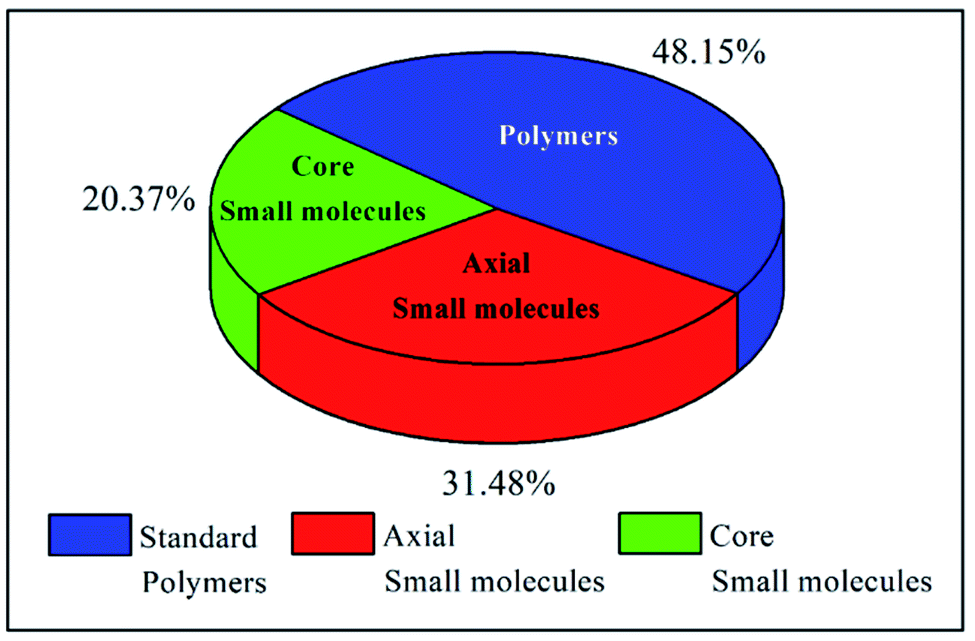 | ||
| Fig. 10 The ratio of types of reported materials. | ||
In terms of device performance, the PCE of devices using small molecule ETLs is slightly better than the efficiency numbers based on polymeric targets, but this is early days and further increases in efficiency need to be seen to break the current ceiling (Fig. 11).
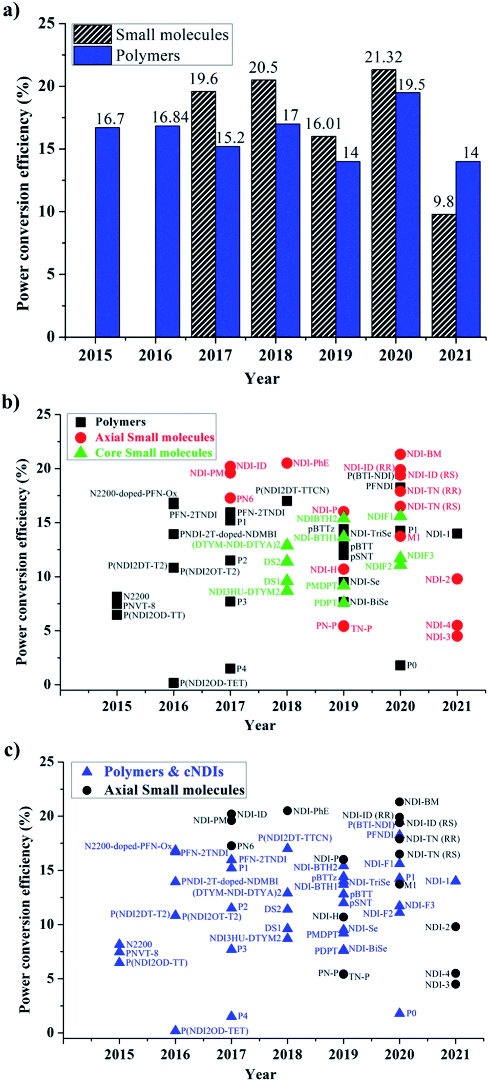 | ||
| Fig. 11 (a) The maximum PCE numbers reported using polymeric and small molecule targets; (b) an inter-relational plot to represent the comparative PCE values of polymers, and small molecules over time; (c) an inter-relational plot of core vs. axial substitution over the same time scale. | ||
The challenges still lie in defining which principle dominates in which situation. For example, the maximum efficiency for a small molecule target (20.5%) employed an axially substituted yet simple NDI derivative, NDI-PhE, as an ETL material.121 In contrast, the maximum efficiency gained for a polymeric NDI target (18.25%) was achieved in the conjugated polymer PFNDI, which is orthogonally substituted to NDI-PhE through a cNDI motif, bearing highly soluble branched and straight chain alkyl groups with phosphite esters.114 As opposed to the representative polymer examples, the design of small molecules can be easily sub-categorized into axial and core substituted geometries. Although the number of structures based on axial substitution are slightly higher than those of core substituted ones (Fig. 10) and with respect to the highly efficient PSCs using these ETL materials in this review, no clear direction is yet to be made for a preferred design. We further realise that aryl/heteroaryl N-substituted NDI derivatives have not been reported for PSCs and this may be due to insolubility that such compounds can be expected to have. For example, the direct connection of functionalities, such as pyridine, pyrimidine and triazine, to name a few, at axial positions has not been reported, though the target materials seem to be promising candidates as ETL materials based on the results reported in this review. Fig. 11c makes an interesting comparison of axial-substituted small molecules to core substituted examples of both small molecule and polymer types. A less clear differentiation for the need of polymers is seen through this comparison. To date, most organic ETL materials derived from NDIs were fabricated using an inverted device architecture, where the ETL is cast over the perovskite layer. This is reasonable, given the perovskite layer is fabricated using dipolar aprotic solvents, such as dimethylformamide and dimethyl sulfoxide, and the use of orthogonal solvents to lay ETLs on top of the active layer does not affect the surface morphology. A variety of orthogonal solvents, e.g. chlorobenzene, 1,2-dichlorobenzene, toluene, and xylene, have been reported, suggesting that the newly designed materials should possess adequate solubility in a variety of routinely used solvents to promote current protocols. This is one of the major advantages associated with the use of organic ETL materials as they can be structurally tuned to enhance solubility when compared with the conventional (PC61BM) and inorganic (metal oxides) ETL materials. This is particularly true for NDI-based ETL materials as these materials can be designed with a variety of alkyl, alkoxy and polyethylene glycol chains at imide nitrogen atoms to boost their solution processability and hence to exhibit a good film-forming ability as shown throughout (Fig. 8 and 9).
Given the fact that solubility is a vital prerequisite for an ETL material, practically all the ETLs discussed thus far have been deposited via solution-processable techniques, and spin-coating in particular. Another method that is worth exploring, albeit less investigated, is vacuum deposition, which can be realised through thermal evaporation.132 The advantages may include, (1) excellent surface constancy that may fully cover the perovskite layer, which is useful for textured substrates for example, (2) low ETL surface roughness, (3) enhanced electron mobility, and (4) an ability to process a large number of materials which are otherwise insoluble in orthogonal solvents, thus, avoiding all the environmental unfriendly, toxic solvents.133 Nakamura reported the potential of NDI-H as a transparent ETL material122 and generated thermally converted and vacuum-deposited electron extraction layers. The PSCs exhibited 4.8% and 10.7% efficiencies with thermally converted and vacuum deposited NDI-H layers, respectively. The latter efficiency number was comparable to the efficiency achieved using a C60 ETL in the same device architecture (9.3%). Moreover, the vacuum-deposited film of NDI-H was observed to have lesser crystallinity than the thermally converted film, suggesting that the low ETL surface roughness can be the key to achieve higher device outcome and that the vacuum deposition technique is worth exploring. The challenge is to ensure the stability and sublimation characteristics of NDIs. According to the literature reviewed, most of the reported materials exhibit the former, i.e. very high decomposition temperature, which, according to some claims, is beneficial for the PSCs, particularly in terms of the devices' temporal stability. Many of the papers reported on device thermal stability and concluded that ETL materials based on NDI format are excellent candidates that can help to improve thermal and overall stability of PSC devices. There is another observation that is be made with respect to the requirement for high electron mobility in ETL materials. Many of the reported materials also exhibit high electron mobilities in the magnitude range of 10−4 cm2 V−1 s−1, which is comparable to that of the conventionally used PC61BM (∼10−3 cm2 V−1 s−1) as opposed to inorganic ETLs such as TiO2, and appear to be a strong requirement.134
Overall, any newly designed organic materials, irrespective of polymers or small molecule, should fulfil a number of requirements to be ideal electron extraction layer materials for PSCs including, high purity, well-tuned HOMO/LUMO energy levels, amorphous nature, good electron mobility, and an ability to interact chemically with the perovskite layer (see Fig. 12). In terms of molecular design, a number of parameters including, (1) extended conjugation with the use of a variety of building blocks such as donor and acceptor, (2) inclusion of lipophilic chains at imide nitrogen atoms, (3) incorporation of functional units containing heteroatoms such as nitrogen and sulfur, and (4) insertion of chiral centres in the solubilising side chains to limit aggregation, can be considered.
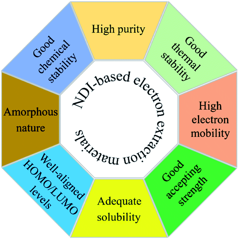 | ||
| Fig. 12 Features required of efficient, NDI-based n-type materials for use as ETLs. | ||
5. Conclusions and outlook
This review summarizes recent literature reports on electron extraction layer materials based on the NDI molecular structure that have been used as essential components in PSCs, regardless of cell architecture. In this review, we categorized ETL materials into (3.1) polymers and (3.2) small molecules (Fig. 11). The latter was further classified into (3.2.1) axial- and (3.2.2) core-substituted categories. We reviewed the use of a variety of target structures that were generated using the combination of a variety of building blocks, such as donor and acceptors blocks. These blocks are essential components to generate highly conjugated targets, i.e. both polymers or core-substituted small molecules, and their structures were amended to satisfy a number of features, e.g. energy levels, solubility, and thermal stability, required of target materials.81,82 It became evident that axial substitution is potentially a better design feature to examine when compared with substitutions based on the core. Generally, core-substituted NDIs are more difficult to produce, require complex purification strategies, and provide lower efficiencies. We also reported device designs, PSC efficiencies, and comparative performance using the conventional ETL materials. We tabulated device parameters including electron mobility values in Tables 1 and 2.It is evident from our review that an important area of investigation is the continuation of research on the design and development of inexpensive and efficient ETL materials, and that NDI-based materials show promise as an alternative to the conventional and widely reported materials, e.g. the inorganic metal oxides, TiO2, SnO2 and ZnO, as well as the fullerene-based PC61BM and C60, which can be expensive and processed with the environmentally unfriendly, toxic solvents. Although effective for achieving high cell PCE, the conventionally used PC61BM or C60 not only are expensive but suffer from restricted chemical and energetic tuning via structural modification. Such disadvantages encourage researchers to seek alternative structural types which can be easily synthesized, scaled-up and compete with the conventionally used PC61BM or C60 by keeping desirable properties such as high electron mobility, solubility, chemical and thermal stabilities and excellent accepting strength. One of such alternative structural types is the NDI-based materials discussed in this review which can certainly exhibit key properties such as good accepting strength, extended conjugation for excellent electron mobility, tuned energy levels and structural diversity. Moreover, these NDI-based targets can be prepared using facile synthetic processes, in high-yield and with high purity, possess excellent electron mobility, and can be structurally tuned to possess complementary energy levels. Furthermore, NDI-based ETLs can be deposited uniformly and reproducibly over large areas using an industrially scalable methodology, e.g. doctor blading or slot die coating, if the commercial application is intended for PSCs. Finally, the ETL materials based on NDI format can have high thermal and environmental stabilities (i.e., no phase transitions below 250 °C), thus, leading to long-term temporal stability in PSCs. The requirements of NDI-based target materials are summarised in Fig. 12. This review presents a timely account of recent reports for NDI-based ETL materials and provides insight into the structural aspects that are crucial to designing next-generation, highly efficient electron extraction materials for stable PSC devices.
Conflicts of interest
There are no conflicts to declare.Acknowledgements
The authors acknowledge the funding support from the School of Science, Computing and Engineering Technology, Swinburne University of Technology. M. Jameel acknowledges PhD scholarship under the Swinburne University Postgraduate Research Award (SUPRA) program and PhD top-up scholarship from the Energy Technologies program, CSIRO Energy, NSW Australia. The CSIRO Division of Manufacturing, Clayton, Victoria Australia is acknowledged for providing support through a Visiting Scientist position for A. G. Authors T. C. J.-Y. and G. J. W. wish to thank the CSIRO Research Office and the Energy Technologies program for project funding, postgraduate scholarships, and fellowship support.References
- H. D. Pham, T. C.-J. Yang, S. M. Jain, G. J. Wilson and P. Sonar, Adv. Energy Mater., 2020, 10, 1903326 CrossRef CAS
.
-
I. E. Agency, World Energy Outlook 2018, p. 661, https://webstore.iea.org/world-energy-outlook-2018 Search PubMed
- T. M. L. Wigley and S. C. B. Raper, Science, 2001, 293, 451–454 CrossRef CAS PubMed
- J. C. Orr, V. J. Fabry, O. Aumont, L. Bopp, S. C. Doney, R. A. Feely, A. Gnanadesikan, N. Gruber, A. Ishida, F. Joos, R. M. Key, K. Lindsay, E. Maier-Reimer, R. Matear, P. Monfray, A. Mouchet, R. G. Najjar, G.-K. Plattner, K. B. Rodgers, C. L. Sabine, J. L. Sarmiento, R. Schlitzer, R. D. Slater, I. J. Totterdell, M.-F. Weirig, Y. Yamanaka and A. Yool, Nature, 2005, 437, 681–686 CrossRef CAS PubMed
- T.-J. Kim, Open J. Earthq. Res., 2018, 7, 195–219 CrossRef
- A. E. Becquerel, C. R. Acad. Sci., 1839, 561–567 Search PubMed
- D. M. Chapin, C. S. Fuller and G. L. Pearson, J. Appl. Phys., 1954, 25, 676–677 CrossRef CAS
- M. A. Green, K. Emery, Y. Hishikawa, W. Warta and E. D. Dunlop, Prog. Photovoltaics, 2012, 20, 606–614 Search PubMed
- M. A. Green, Semicond. Sci. Technol., 1993, 8, 1–12 CrossRef CAS
-
V. P. Equipment, International Technology Roadmap for Photovoltaic (ITRPV) 2019, Germany, 2020 Search PubMed
- M. A. Green, Sol. Energy Mater. Sol. Cells, 2015, 143, 190–197 CrossRef CAS
- C. W. Tang, Appl. Phys. Lett., 1986, 48, 183–185 CrossRef CAS
- N. S. Sariciftci, L. Smilowitz, A. J. Heeger and F. Wudl, Science, 1992, 258, 1474–1476 CrossRef CAS PubMed
- Y. Wang, Nature, 1992, 356, 585–587 CrossRef CAS
- J. J. M. Halls, C. A. Walsh, N. C. Greenham, E. A. Marseglia, R. H. Friend, S. C. Moratti and A. B. Holmes, Nature, 1995, 376, 498–500 CrossRef CAS
- G. Yu, J. Gao, J. C. Hummelen, F. Wudl and A. J. Heeger, Science, 1995, 270, 1789–1791 CrossRef CAS
- B. O'Regan and M. Grätzel, Nature, 1991, 353, 737–740 CrossRef
- R. F. Service, Science, 2014, 344, 458 CrossRef PubMed
-
C. Eberspacher, J. Ermer, C. Fredric, C. Jensen, R. Gay, D. Pier, D. Willett and F. Karg, Recent Advances in Single-Junction and Tandem Thin Film Modules Based On CuInSe2, Dordrecht, 1991 Search PubMed
-
M. Green, Third Generation Photovoltaics, Springer-Verlag Berlin Heidelberg, 2003 Search PubMed
- G. Conibeer, Mater. Today, 2007, 10, 42–50 CrossRef CAS
- M. Green, E. Dunlop, J. Hohl-Ebinger, M. Yoshita, N. Kopidakis and X. Hao, Prog. Photovoltaics, 2021, 29, 3–15 Search PubMed
- A. Mishra and P. Bäuerle, Angew. Chem., Int. Ed., 2012, 51, 2020–2067 CrossRef CAS PubMed
- R. V. Hangarge, A. Gupta, A. M. Raynor, D. D. La, A. Bilic, J. Li, D. S. Dalal, R. A. Evans and S. V. Bhosale, Dyes Pigm., 2017, 137, 126–134 CrossRef CAS
-
S. Economopoulos, G. Itskos, P. Koutentis and S. Choulis, Overview of Polymer and Copolymer Materials for Organic Photovoltaics, ed. C. Brabec, U. Scherf and V. Dyakonov, Wiley Online Library, 2014, pp. 3–26, DOI:10.1002/9783527656912.ch01
- C. J. Brabec, Sol. Energy Mater. Sol. Cells, 2004, 83, 273–292 CrossRef CAS
- J. Jean, P. R. Brown, R. L. Jaffe, T. Buonassisi and V. Bulović, Energy Environ. Sci., 2015, 8, 1200–1219 RSC
- P. K. Nayak, S. Mahesh, H. J. Snaith and D. Cahen, Nat. Rev. Mater., 2019, 4, 269–285 CrossRef CAS
- S. S. Mali and C. K. Hong, Nanoscale, 2016, 8, 10528–10540 RSC
- A. Kojima, K. Teshima, Y. Shirai and T. Miyasaka, J. Am. Chem. Soc., 2009, 131, 6050–6051 CrossRef CAS PubMed
- J. H. Im, C. R. Lee, J. W. Lee, S. W. Park and N. G. Park, Nanoscale, 2011, 3, 4088–4093 RSC
- H. S. Kim, C. R. Lee, J. H. Im, K. B. Lee, T. Moehl, A. Marchioro, S. J. Moon, R. Humphry-Baker, J. H. Yum, J. E. Moser, M. Grätzel and N. G. Park, Sci. Rep., 2012, 2, 591 CrossRef PubMed
- M. M. Lee, J. Teuscher, T. Miyasaka, T. N. Murakami and H. J. Snaith, Science, 2012, 338, 643 CrossRef CAS PubMed
-
NREL, Best Research-Cell Efficiencies, https://www.nrel.gov/pv/cell-efficiency.html, accessed September, 2020 Search PubMed
- Editorial, Nat. Energy, 2019, 4, 1, DOI:10.1038/s41560-018-0323-9.
- M. Jeong, I. W. Choi, E. M. Go, Y. Cho, M. Kim, B. Lee, S. Jeong, Y. Jo, H. W. Choi, J. Lee, J.-H. Bae, S. K. Kwak, D. S. Kim and C. Yang, Science, 2020, 369, 1615–1620 CrossRef CAS PubMed
- H.-S. Kim, J.-W. Lee, N. Yantara, P. P. Boix, S. A. Kulkarni, S. Mhaisalkar, M. Grätzel and N.-G. Park, Nano Lett., 2013, 13, 2412–2417 CrossRef CAS PubMed
- A. Yella, L.-P. Heiniger, P. Gao, M. K. Nazeeruddin and M. Grätzel, Nano Lett., 2014, 14, 2591–2596 CrossRef CAS PubMed
- L. Lin, T. W. Jones, T. C.-J. Yang, N. W. Duffy, J. Li, L. Zhao, B. Chi, X. Wang and G. J. Wilson, Adv. Funct. Mater., 2021, 31, 2008300 CrossRef CAS
- T. Leijtens, G. E. Eperon, S. Pathak, A. Abate, M. M. Lee and H. J. Snaith, Nat. Commun., 2013, 4, 2885 CrossRef PubMed
- J. Song, E. Zheng, J. Bian, X.-F. Wang, W. Tian, Y. Sanehira and T. Miyasaka, J. Mater. Chem. A, 2015, 3, 10837–10844 RSC
- S. V. Bhosale, M. Al Kobaisi, R. W. Jadhav, P. P. Morajkar, L. A. Jones and S. George, Chem. Soc. Rev., 2021, 1–145, DOI:10.1002/aenm.201903326
- A. Seitkhan, M. Neophytou, M. Kirkus, E. Abou-Hamad, M. N. Hedhili, E. Yengel, Y. Firdaus, H. Faber, Y. Lin, L. Tsetseris, I. McCulloch and T. D. Anthopoulos, Adv. Funct. Mater., 2019, 29, 1905810 CrossRef CAS
- S. Wu, Z. Li, M.-Q. Li, Y. Diao, F. Lin, T. Liu, J. Zhang, P. Tieu, W. Gao, F. Qi, X. Pan, Z. Xu, Z. Zhu and A. K. Y. Jen, Nat. Nanotechnol., 2020, 15, 934–940 CrossRef CAS PubMed
- A. A. Said, J. Xie and Q. Zhang, Small, 2019, 15, 1900854 CrossRef PubMed
- K. Mahmood, S. Sarwar and M. T. Mehran, RSC Adv., 2017, 7, 17044–17062 RSC
- M. Cheng, C. Zuo, Y. Wu, Z. Li, B. Xu, Y. Hua and L. Ding, Sci. Bull., 2020, 65, 1237–1241 CrossRef CAS
- U. Bach, D. Lupo, P. Comte, J. E. Moser, F. Weissörtel, J. Salbeck, H. Spreitzer and M. Grätzel, Nature, 1998, 395, 583–585 CrossRef CAS
- Q. Wang, C. Bi and J. Huang, Nano Energy, 2015, 15, 275–280 CrossRef CAS
- Y. Xia and S. Dai, J. Mater. Sci.: Mater. Electron., 2020, 32, 12746–12757 CrossRef
- T. Wang, D. Ding, H. Zheng, X. Wang, J. Wang, H. Liu and W. Shen, Sol. RRL, 2019, 3, 1900045 CrossRef
- M. S. White, D. C. Olson, S. E. Shaheen, N. Kopidakis and D. S. Ginley, Appl. Phys. Lett., 2006, 89, 143517 CrossRef
- F. Eisner, A. Seitkhan, Y. Han, D. Khim, E. Yengel, A. R. Kirmani, J. Xu, F. P. García de Arquer, E. H. Sargent, A. Amassian, Z. Fei, M. Heeney and T. D. Anthopoulos, Sol. RRL, 2018, 2, 1800076 CrossRef
- M. K. Siddiki, S. Venkatesan and Q. Qiao, Phys. Chem. Chem. Phys., 2012, 14, 4682–4686 RSC
- L. Lin, T. W. Jones, T. C.-J. Yang, N. W. Duffy, J. Li, L. Zhao, B. Chi, X. Wang and G. J. Wilson, Adv. Funct. Mater., 2021, 31, 2008300 CrossRef CAS
- N. Wang, J. Yu, Y. Zang, J. Huang and Y. Jiang, Sol. Energy Mater. Sol. Cells, 2010, 94, 263–266 CrossRef CAS
- Z. He, H. Wu and Y. Cao, Adv. Mater. Interfaces, 2014, 26, 1006–1024 CrossRef CAS PubMed
- Y. Cai, L. Chang, L. You, B. Fan, H. Liu and Y. Sun, ACS Appl. Mater. Interfaces, 2018, 10, 24082–24089 CrossRef CAS PubMed
- C. J. Brabec, A. Cravino, D. Meissner, N. S. Sariciftci, T. Fromherz, M. T. Rispens, L. Sanchez and J. C. Hummelen, Adv. Funct. Mater., 2001, 11, 374–380 CrossRef CAS
- S. S. Birajdar, S. Brixi, P. S. Rao, R. S. Bhosale, M. A. Kobaisi, A. Gupta, B. H. Lessard, S. V. Bhosale and S. V. Bhosale, ChemistryOpen, 2021, 10, 414–420 CrossRef CAS PubMed
- S. M. Wagalgave, S. V. Bhosale, R. S. Bhosale, A. L. Puyad, J.-Y. Chen, J.-L. Li, R. A. Evans, A. Gupta and S. V. Bhosale, Mater. Chem. Front., 2019, 3, 1231–1237 RSC
- D. Srivani, A. Gupta, S. V. Bhosale, A. L. Puyad, W. Xiang, J. Li, R. A. Evans and S. V. Bhosale, Chem. Commun., 2017, 53, 7080–7083 RSC
- H. D. Pham, T. C.-J. Yang, S. M. Jain, G. J. Wilson and P. Sonar, Adv. Energy Mater., 2020, 10, 2070057 CrossRef CAS
- J. Urieta-Mora, I. García-Benito, A. Molina-Ontoria and N. Martín, Chem. Soc. Rev., 2018, 47, 8541–8571 RSC
- E. Rezaee, X. Liu, Q. Hu, L. Dong, Q. Chen, J.-H. Pan and Z.-X. Xu, Sol. RRL, 2018, 2, 1800200 CrossRef
- Z. Zhu, Y. Bai, X. Liu, C.-C. Chueh, S. Yang and A. K. Y. Jen, Adv. Mater. Interfaces, 2016, 28, 6478–6484 CrossRef CAS PubMed
- K. Yan, J. Chen, H. Ju, F. Ding, H. Chen and C.-Z. Li, J. Mater. Chem. A, 2018, 6, 15495–15503 RSC
- Q. Hu, W. Chen, W. Yang, Y. Li, Y. Zhou, B. W. Larson, J. C. Johnson, Y.-H. Lu, W. Zhong, J. Xu, L. Klivansky, C. Wang, M. Salmeron, A. B. Djurišić, F. Liu, Z. He, R. Zhu and T. P. Russell, Joule, 2020, 4, 1575–1593 CrossRef CAS
- L. Li, H. Chen, Z. Fang, X. Meng, C. Zuo, M. Lv, Y. Tian, Y. Fang, Z. Xiao, C. Shan, Z. Xiao, Z. Jin, G. Shen, L. Shen and L. Ding, Adv. Mater., 2020, 32, 1907257 CrossRef CAS PubMed
- C. Chen, C. Wu, X. Ding, Y. Tian, M. Zheng, M. Cheng, H. Xu, Z. Jin and L. Ding, Nano Energy, 2020, 71, 104604 CrossRef CAS
- M. Zheng, Y. Miao, A. A. Syed, C. Chen, X. Yang, L. Ding, H. Li and M. Cheng, J. Energy Chem., 2021, 56, 374–382 CrossRef
- G. Andric, J. F. Boas, A. M. Bond, G. D. Fallon, K. P. Ghiggino, C. F. Hogan, J. A. Hutchison, M. A.-P. Lee, S. J. Langford, J. R. Pilbrow, G. J. Troup and C. P. Woodward, Aust. J. Chem., 2004, 57, 1011–1019 CrossRef CAS
- S. V. Bhosale, M. B. Kalyankar, S. V. Bhosale, S. J. Langford, E. F. Reid and C. F. Hogan, New J. Chem., 2009, 33, 2409–2413 RSC
- N. Banerji, S. V. Bhosale, I. Petkova, S. J. Langford and E. Vauthey, Phys. Chem. Chem. Phys., 2011, 13, 1019–1029 RSC
- H. F. Higginbotham, S. Maniam, S. J. Langford and T. D. M. Bell, Dyes Pigm., 2015, 112, 290–297 CrossRef CAS
- D. H. Gharib, P. Lock, S. E. Moulton, F. Malherbe and S. J. Langford, ChemNanoMat, 2019, 5, 1303–1310 CrossRef CAS
- S. Ali, M. A. Jameel, A. Gupta, S. J. Langford and M. Shafiei, Synth. Met., 2021, 275, 116739 CrossRef CAS
- S. Ali, M. A. Jameel, C. J. Harrison, A. Gupta, M. Shafiei and S. J. Langford, Sens. Actuators, B, 2022, 351, 130972 CrossRef CAS
- P. S. Rao, A. Gupta, D. Srivani, S. V. Bhosale, A. Bilic, J. Li, W. Xiang, R. A. Evans and S. V. Bhosale, Chem. Commun., 2018, 54, 5062–5065 RSC
- D. Srivani, A. Agarwal, S. V. Bhosale, A. L. Puyad, W. Xiang, R. A. Evans, A. Gupta and S. V. Bhosale, Chem. Commun., 2017, 53, 11157–11160 RSC
- S. Maniam, H. F. Higginbotham, T. D. M. Bell and S. J. Langford, Chem.–Eur. J., 2019, 25, 7044–7057 CrossRef CAS PubMed
- A. Insuasty, S. Maniam and S. J. Langford, Chem.–Eur. J., 2019, 25, 7058–7073 CrossRef CAS PubMed
- J. Y. Kim, J.-W. Lee, H. S. Jung, H. Shin and N.-G. Park, Chem. Rev., 2020, 120, 7867–7918 CrossRef CAS PubMed
- N. Li, X. Niu, Q. Chen and H. Zhou, Chem. Soc. Rev., 2020, 49, 8235–8286 RSC
- R. Wang, M. Mujahid, Y. Duan, Z.-K. Wang, J. Xue and Y. Yang, Adv. Funct. Mater., 2019, 29, 1808843 CrossRef CAS
- S. Y. Park, J.-S. Park, B. J. Kim, H. Lee, A. Walsh, K. Zhu, D. H. Kim and H. S. Jung, Nat. Sustain., 2020, 3, 1044–1051 CrossRef
- W.-W. Liu, T.-H. Wu, M.-C. Liu, W.-J. Niu and Y.-L. Chueh, Adv. Mater. Interfaces, 2019, 6, 1801758 CrossRef
- G. Schileo and G. Grancini, J. Mater. Chem. C, 2021, 9, 67–76 RSC
- X. Tian, S. D. Stranks and F. You, Sci. Adv., 2020, 6, eabb0055 CrossRef CAS PubMed
- A. Senocrate, G. Y. Kim, M. Grätzel and J. Maier, ACS Energy Lett., 2019, 4, 2859–2870 CrossRef CAS
- S. V. Bhosale, C. H. Jani and S. J. Langford, Chem. Soc. Rev., 2008, 37, 331–342 RSC
- T. D. M. Bell, S. V. Bhosale, C. M. Forsyth, D. Hayne, K. P. Ghiggino, J. A. Hutchison, C. H. Jani, S. J. Langford, M. A. P. Lee and C. P. Woodward, Chem. Commun., 2010, 46, 4881–4883 RSC
- A. K. Hundal, A. Agarwal, M. A. Jameel, S. Ali, J.-Y. Chen, N. Kaur, L. Jones, J.-L. Li, S. J. Langford and A. Gupta, Sol. Energy, 2020, 195, 223–229 CrossRef CAS
- A. K. Hundal, S. Ali, A. Agarwal, M. A. Jameel, L. A. Jones, J.-L. Li, R. A. Evans, S. J. Langford and A. Gupta, J. Phys. Chem. Lett., 2021, 10656–10661, DOI:10.1021/acs.jpclett.0c03526
- M. J. Sung, M. Huang, S. H. Moon, T. H. Lee, S. Y. Park, J. Y. Kim, S.-K. Kwon, H. Choi and Y.-H. Kim, Sol. Energy, 2017, 150, 90–95 CrossRef CAS
- Z. Zhang, J. Yuan, Q. Wei and Y. Zou, Front. Chem., 2018, 6, 414 CrossRef PubMed
- J. Wang and X. Zhan, Trends Chem., 2019, 1, 869–881 CrossRef CAS
- K. Rundel, S. Maniam, K. Deshmukh, E. Gann, S. K. K. Prasad, J. M. Hodgkiss, S. J. Langford and C. R. McNeill, J. Mater. Chem. A, 2017, 5, 12266–12277 RSC
- X. Guo, F. S. Kim, M. J. Seger, S. A. Jenekhe and M. D. Watson, Chem. Mater., 2012, 24, 1434–1442 CrossRef CAS
- J. T. E. Quinn, J. Zhu, X. Li, J. Wang and Y. Li, J. Mater. Chem. C, 2017, 5, 8654–8681 RSC
- Y. H. Ha, J. G. Oh, S. Park, S.-K. Kwon, T. K. An, J. Jang and Y.-H. Kim, Org. Electron., 2018, 63, 250–256 CrossRef CAS
- M. Al Kobaisi, S. V. Bhosale, K. Latham, A. M. Raynor and S. V. Bhosale, Chem. Rev., 2016, 116, 11685–11796 CrossRef PubMed
- W. Wang, J. Yuan, G. Shi, X. Zhu, S. Shi, Z. Liu, L. Han, H.-Q. Wang and W. Ma, ACS Appl. Mater. Interfaces, 2015, 7, 3994–3999 CrossRef CAS PubMed
- C. Sun, Z. Wu, H.-L. Yip, H. Zhang, X.-F. Jiang, Q. Xue, Z. Hu, Z. Hu, Y. Shen, M. Wang, F. Huang and Y. Cao, Adv. Energy Mater., 2016, 6, 1501534 CrossRef
- C. M. Wolff, P. Caprioglio, M. Stolterfoht and D. Neher, Adv. Mater. Interfaces, 2019, 31, 1902762 CrossRef CAS PubMed
- S. Shao, Z. Chen, H. H. Fang, G. H. ten Brink, D. Bartesaghi, S. Adjokatse, L. J. A. Koster, B. J. Kooi, A. Facchetti and M. A. Loi, J. Mater. Chem. A, 2016, 4, 2419–2426 RSC
- Z. Zhu, C.-C. Chueh, G. Zhang, F. Huang, H. Yan and A. K.-Y. Jen, ChemSusChem, 2016, 9, 2586–2591 CrossRef CAS PubMed
- Y. Guo, W. Sato, K. Inoue, W. Zhang, G. Yu and E. Nakamura, J. Mater. Chem. A, 2016, 4, 18852–18856 RSC
- D. Li, C. Sun, H. Li, H. Shi, X. Shai, Q. Sun, J. Han, Y. Shen, H.-L. Yip, F. Huang and M. Wang, Chem, 2017, 8, 4587–4594 CAS
- T. Jia, C. Sun, R. Xu, Z. Chen, Q. Yin, Y. Jin, H.-L. Yip, F. Huang and Y. Cao, ACS Appl. Mater. Interfaces, 2017, 9, 36070–36081 CrossRef CAS PubMed
- H. I. Kim, M.-J. Kim, K. Choi, C. Lim, Y.-H. Kim, S.-K. Kwon and T. Park, Adv. Energy Mater., 2018, 8, 1702872 CrossRef
- A. A. Said, J. Xie, Y. Wang, Z. Wang, Y. Zhou, K. Zhao, W.-B. Gao, T. Michinobu and Q. Zhang, Small, 2019, 15, 1803339 CrossRef PubMed
- W. Yan, Z. Wang, Y. Gong, S. Guo, J. Jiang, J. Chen, C. Tang, R. Xia, W. Huang and H. Xin, Org. Electron., 2019, 67, 208–214 CrossRef CAS
- C. Deng, L. Wan, S. Li, L. Tao, S.-n. Wang, W. Zhang, J. Fang, Z. Fu and W. Song, Org. Electron., 2020, 87, 105959 CrossRef CAS
- Y. Shi, W. Chen, Z. Wu, Y. Wang, W. Sun, K. Yang, Y. Tang, H. Y. Woo, M. Zhou, A. B. Djurišić, Z. He and X. Guo, J. Mater. Chem. A, 2020, 8, 13754–13762 RSC
- S. Valero, A. Cabrera-Espinoza, S. Collavini, J. Pascual, N. Marinova, I. Kosta and J. L. Delgado, Eur. J. Org. Chem., 2020, 2020, 5329–5339 CrossRef CAS
- K. Al Kurdi, D. P. McCarthy, D. P. McMeekin, S. O. Furer, M.-H. Tremblay, S. Barlow, U. Bach and S. R. Marder, Mater. Chem. Front., 2021, 5, 450–457 RSC
- S. Peng, J. Miao, I. Murtaza, L. Zhao, Z. Hu, M. Liu, T. Yang, Y. Liang, H. Meng and W. Huang, J. Mater. Chem. C, 2017, 5, 5949–5955 RSC
- J. H. Heo, S.-C. Lee, S.-K. Jung, O. P. Kwon and S. H. Im, J. Mater. Chem. A, 2017, 5, 20615–20622 RSC
- S.-K. Jung, J. H. Heo, D. W. Lee, S.-C. Lee, S.-H. Lee, W. Yoon, H. Yun, S. H. Im, J. H. Kim and O.-P. Kwon, Adv. Funct. Mater., 2018, 28, 1800346 CrossRef
- S.-K. Jung, J. H. Heo, D. W. Lee, S.-H. Lee, S.-C. Lee, W. Yoon, H. Yun, D. Kim, J. H. Kim, S. H. Im and O.-P. Kwon, ChemSusChem, 2019, 12, 224–230 CrossRef CAS PubMed
- T. Nakamura, N. Shioya, T. Shimoaka, R. Nishikubo, T. Hasegawa, A. Saeki, Y. Murata, R. Murdey and A. Wakamiya, Chem. Mater., 2019, 31, 1729–1737 CrossRef CAS
- L. Li, Y. Wu, E. Li, C. Shen, H. Zhang, X. Xu, G. Wu, M. Cai and W.-H. Zhu, Chem. Commun., 2019, 55, 13239–13242 RSC
- S. Y. Kim, S. J. Cho, S. E. Byeon, X. He and H. J. Yoon, Adv. Energy
Mater., 2020, 10, 2002606 CrossRef CAS
- S.-K. Jung, J. H. Heo, B. M. Oh, J. B. Lee, S.-H. Park, W. Yoon, Y. Song, H. Yun, J. H. Kim, S. H. Im and O.-P. Kwon, Adv. Funct. Mater., 2020, 30, 1905951 CrossRef CAS
- J. Ning, Y. Zhu, Z. Hu, Y. Shi, M. U. Ali, J. He, Y. He, F. Yan, S. Yang, J. Miao and H. Meng, Adv. Funct. Mater., 2020, 30, 2000837 CrossRef CAS
- C. Ge, W. Wu, L. Hu, Y. Hu, Y. Zhou, W.-S. Li and X. Gao, Org. Electron., 2018, 61, 113–118 CrossRef CAS
- A. A. Said, S. M. Wagalgave, J. Xie, A. L. Puyad, W. Chen, Z. Wang, S. V. Bhosale, S. V. Bhosale and Q. Zhang, J. Solid State Chem., 2019, 270, 51–57 CrossRef CAS
- D. B. Shaikh, A. A. Said, R. S. Bhosale, W. Chen, S. V. Bhosale, A. L. Puyad, S. V. Bhosale and Q. Zhang, Asian J. Org. Chem., 2018, 7, 2294–2301 CrossRef CAS
- D. B. Shaikh, A. Ali Said, Z. Wang, P. Srinivasa Rao, R. S. Bhosale, A. M. Mak, K. Zhao, Y. Zhou, W. Liu, W. Gao, J. Xie, S. V. Bhosale, S. V. Bhosale and Q. Zhang, ACS Appl. Mater. Interfaces, 2019, 11, 44487–44500 CrossRef CAS PubMed
- W. Liu, D. B. Shaikh, P. S. Rao, R. S. Bhosale, A. A. Said, A. M. Mak, Z. Wang, M. Zhao, W. Gao, B. Chen, Y. M. Lam, W. Fan, S. V. Bhosale, S. V. Bhosale and Q. Zhang, Chem.–Asian J., 2020, 15, 112–121 CrossRef CAS PubMed
- Y. Vaynzof, Adv. Energy Mater., 2020, 10, 2003073 CrossRef CAS
- R. Vidal, J.-A. Alberola-Borràs, S. N. Habisreutinger, J.-L. Gimeno-Molina, D. T. Moore, T. H. Schloemer, I. Mora-Seró, J. J. Berry and J. M. Luther, Nat. Sustain., 2021, 4, 277–285 CrossRef
- T. Bak, M. K. Nowotny, L. R. Sheppard and J. Nowotny, J. Phys. Chem. C, 2008, 112, 12981–12987 CrossRef CAS
Footnotes |
| † Present address: Department of Chemical Engineering and Biotechnology, University of Cambridge, Cambridge, UK. |
| ‡ Present address: Cavendish Laboratory, Department of Physics, University of Cambridge, Cambridge, UK. |
| This journal is © The Royal Society of Chemistry 2021 |