DOI:
10.1039/D1TA02968A
(Communication)
J. Mater. Chem. A, 2021,
9, 19613-19618
Oriented growth of semiconducting TCNQ@Cu3(BTC)2 MOF on Cu(OH)2: crystallographic orientation and pattern formation toward semiconducting thin-film devices†
Received
9th April 2021
, Accepted 2nd June 2021
First published on 4th June 2021
Abstract
The host–guest system TCNQ@Cu3(BTC)2 (TCNQ = 7,7,8,8-tetracyanoquinodimethane, BTC = 1,3,5-benzenetricarboxylate) exhibits semiconducting properties with potential applications in thin-film devices, such as field-effect transistors and thermoelectric films. Although controlling its crystallographic orientation is important for the efficient use of its electrical properties in advanced semiconductors, the fabrication of Cu3(BTC)2 thin films with both in-plane and out-of-plane orientations (three-dimensionally oriented thin films) remains a challenge. Here, we report on the fabrication of three-dimensionally oriented Cu3(BTC)2 thin films via heteroepitaxial growth on Cu(OH)2. The epitaxial growth direction of Cu3(BTC)2 is determined by lattice matching at the Cu3(BTC)2/Cu(OH)2 interface and interface bonding (local chemical connection matching; spatial matching of Cu atoms across the interface). The epitaxial growth approach enables the fabrication of oriented TCNQ@Cu3(BTC)2 thin films, where the {111} lattice plane, which can be a conducting path, is oriented both parallel and perpendicular to the substrate. Owing to the in-plane orientation of the {111} lattice plane in the oriented TCNQ@Cu3(BTC)2 film, we have, for the first time, achieved MOF thin films with anisotropic electrical properties in the in-plane direction. Moreover, we show that it is possible to fabricate oriented MOF patterns by integration with UV lithography technology. The oriented MOF patterns with anisotropic conduction will pave the way for next-generation smart electronic devices.
1. Introduction
Metal–organic frameworks (MOFs), also called porous coordination polymers, are crystalline porous organic–inorganic hybrid materials consisting of metal-based nodes and organic linkers via coordination bonds.1,2 Because of their periodic frameworks as well as structural and chemical versatility, MOFs are being developed for bulk applications, such as gas storage and engineering operations (catalysis, separation).3–6 More recently, the potential applications of MOFs have focused on high-value technological areas (e.g., thin-film devices) because of their “designable” electrical properties that benefit from the ordered micropores and frameworks, and are unprecedented in other materials. These include short- and long-range ordered micropores, metal-based nodes and organic linkers, and versatile host–guest chemistry (“guest@MOF” properties), as introduced in recent review articles.7–12 However, most MOFs exhibit poor electrical conductivity because of the insulating organic ligands and poor overlap between the atomic orbitals of metal ions. In 2014, Talin et al. reported a promising host–guest system that affects the electrical conductivity of MOFs. The infiltration of insulating Cu3(BTC)2 MOF (also known as HKUST-1, BTC = 1,3,5-benzenetricarboxylate) by the redox-active guest molecule 7,7,8,8-tetracyanoquinodimethane (TCNQ) (TCNQ@Cu3(BTC)2) increased its conductivity by six orders of magnitude from 10−8 to 0.07 S cm−1.13 It was proposed that conducting pathways were formed in TCNQ@Cu3(BTC)2 when TCNQ bridged the two neighbouring Cu-paddlewheels.13 Its semiconducting properties make TCNQ@Cu3(BTC)2 a novel and promising material for thin-film devices, such as micro-electronic devices, sensors, and thermoelectric devices.14–16 The conducting path is known to exist along the {111} lattice plane of TCNQ@Cu3(BTC)2; this is supported by both theoretical and experimental data.13,17 Therefore, a key concern is the fabrication of thin films with controlled orientation, especially {111} lattice planes of Cu3(BTC)2, for sophisticated thin-film devices. The use of substrates modified with self-assembled monolayers (SAMs) is one of the most widely used methods for fabricating oriented MOF thin films.18–21 In this method, the lattice plane parallel to the substrate (out-of-plane orientation) can be controlled by changing the terminated functional group of the SAM. In fact, in semiconducting TCNQ@Cu3(BTC)2 thin films for thin-film devices reported so far, an SAM-modified substrate is employed to fabricate the oriented Cu3(BTC)2 thin film, in which the {111} lattice plane is preferentially oriented parallel to the substrate.13,22,23 However, although existing methods can control the crystallographic orientation along the out-of-plane direction (perpendicular to the substrate), Cu3(BTC)2 thin films with both out-of-plane and in-plane (parallel to the substrate) orientations have not been achieved. The fabrication of Cu3(BTC)2 thin films with both out-of-plane and in-plane orientations is an important step towards realizing MOF-based thin-film devices, as is the case with inorganic material-based semiconductors.
The fabrication of Cu3(BTC)2 thin films with both out-of-plane and in-plane orientations is difficult compared with MOFs with low crystal symmetry (lattice anisotropy, e.g. NU-1000: P6/mmm), whose crystals usually exhibit an anisotropic morphology, such as nanorods and nanosheets.24 Because the Cu3(BTC)2 crystal is isotropic owing to its high crystal symmetry (Fm![[3 with combining macron]](https://www.rsc.org/images/entities/char_0033_0304.gif) m), it is difficult to orient the crystallites towards a specific direction even when external fields (e.g. share force, electric, and magnetic fields) are applied. Therefore, it is scientifically challenging to fabricate Cu3(BTC)2 thin films with both out-of-plane and in-plane orientations. In the present study, we have, for the first time, successfully fabricated Cu3(BTC)2 thin films with both out-of-plane and in-plane orientations by employing an epitaxial growth approach on Cu(OH)2 that we developed.25–29 Both the lattice matching at the Cu3(BTC)2/Cu(OH)2 interface and the interface bonding (local chemical connection matching; spatial matching of Cu atoms across the interface) allow the crystallographic orientation of Cu3(BTC)2. The epitaxial growth approach enables the fabrication of oriented TCNQ@Cu3(BTC)2 thin films, where the {111} lattice plane, which can be a conducting path, is oriented both parallel and perpendicular to the substrate. Owing to the in-plane orientation of the {111} lattice plane in the oriented TCNQ@Cu3(BTC)2 thin film, MOF thin films with anisotropic electrical properties in the in-plane direction were obtained for the first time. We also show that it is possible to fabricate oriented MOF patterns by integration with UV lithography technology. The oriented MOF patterns with anisotropic conduction will pave the way for next-generation smart electronic devices.
m), it is difficult to orient the crystallites towards a specific direction even when external fields (e.g. share force, electric, and magnetic fields) are applied. Therefore, it is scientifically challenging to fabricate Cu3(BTC)2 thin films with both out-of-plane and in-plane orientations. In the present study, we have, for the first time, successfully fabricated Cu3(BTC)2 thin films with both out-of-plane and in-plane orientations by employing an epitaxial growth approach on Cu(OH)2 that we developed.25–29 Both the lattice matching at the Cu3(BTC)2/Cu(OH)2 interface and the interface bonding (local chemical connection matching; spatial matching of Cu atoms across the interface) allow the crystallographic orientation of Cu3(BTC)2. The epitaxial growth approach enables the fabrication of oriented TCNQ@Cu3(BTC)2 thin films, where the {111} lattice plane, which can be a conducting path, is oriented both parallel and perpendicular to the substrate. Owing to the in-plane orientation of the {111} lattice plane in the oriented TCNQ@Cu3(BTC)2 thin film, MOF thin films with anisotropic electrical properties in the in-plane direction were obtained for the first time. We also show that it is possible to fabricate oriented MOF patterns by integration with UV lithography technology. The oriented MOF patterns with anisotropic conduction will pave the way for next-generation smart electronic devices.
2. Results and discussion
2.1 Oriented growth of Cu3(BTC)2 on Cu(OH)2
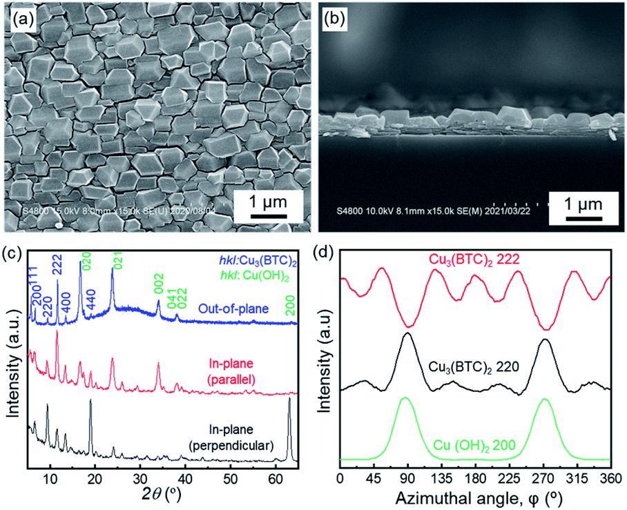
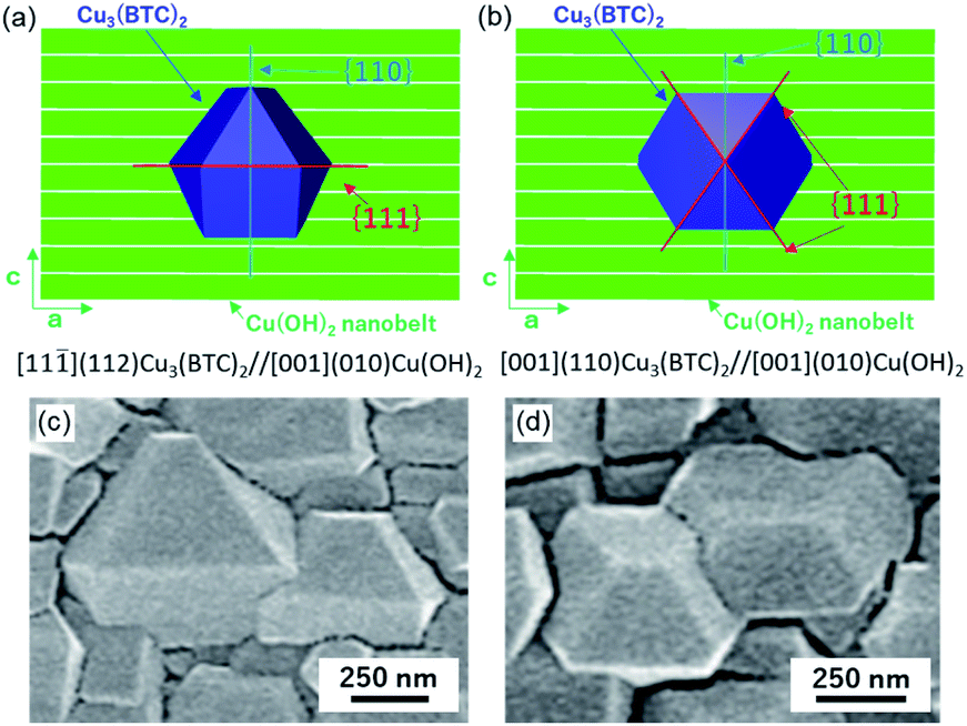
Oriented Cu3(BTC)2 thin films were fabricated on aligned Cu(OH)2 nanobelts via a one-pot method, in which Cu(OH)2 nanobelts oriented on Si substrates were reacted with H3BTC in a water–ethanol mixture (1![[thin space (1/6-em)]](https://www.rsc.org/images/entities/char_2009.gif) :1 vol%) at room temperature for 10 min. After the reaction, homogeneous Cu3(BTC)2 thin films were obtained on the entire surface of the centimetre-scale substrate (see Fig. S1†). The surface of Cu(OH)2 nanobelts was covered with cuboctahedron-shaped crystals, which were observed as Cu3(BTC)2 crystals (Fig. 1a).30 The triangular and square shapes (some missing edges) on the exposed surface of the crystals indicate the {111} and {100} facets, respectively. A cross-sectional scanning electron microscope (SEM) image showed that Cu3(BTC)2 thin films with a thickness of ∼300 nm formed on the Cu(OH)2 nanobelt film, and that Cu3(BTC)2 crystallites were connected to each other (Fig. 1b). Because of the isotropic morphologies of Cu3(BTC)2 crystals, it is difficult to confirm their orientation by SEM images (we can observe the orientation when we focus on the triangular {111} and square {100} facets). The crystallographic structure and orientation of Cu3(BTC)2 were confirmed by X-ray diffraction (XRD) experiments using previously reported protocols, which allow the crystallographic orientation along all three axes to be examined (Fig. 1c).25–29 The diffraction patterns can be attributed to Cu3(BTC)2 and Cu(OH)2 (see Fig. S2†). The intense 222 reflection of Cu3(BTC)2 in the out-of-plane XRD pattern (at 2θ = 11.7°) compared with the powder XRD pattern indicates that the {111} lattice planes of the MOF were preferentially oriented parallel to the substrate. Most reflections, especially 220 and 222 reflections (at 2θ = 9.5° and 11.7°, respectively) detected in both in-plane XRD measurements, show a distinct X-ray incident angular dependence. These results indicate that the {110} and {111} lattice planes of the MOF crystals are aligned orthogonally to each other over the entire surface, and perpendicularly to the substrate. More detailed in-plane orientations of the {110} and {111} lattice planes were investigated by considering the azimuthal angle dependence of the intensity (φ scan) profiles (Fig. 1d). This method provides information on the angular relationship between the selected lattice planes of Cu3(BTC)2 and Cu(OH)2 in the in-plane direction. Intense signals were detected at φ = 90° and φ = 270° for the 200 and 220 reflections of Cu(OH)2 and Cu3(BTC)2, respectively, whereas 222 reflections of Cu3(BTC)2 were detected at approximately φ = 0, 55, 125, 180, 235, 305 and 360°, showing strong angular dependence. The φ scan profiles clearly indicate that the {110} lattice planes of Cu3(BTC)2 are parallel to the {100} lattice planes of Cu(OH)2. On the other hand, the {111} lattice planes of Cu3(BTC)2 are orthogonal to the {100} lattice planes of Cu(OH)2, and at an angle of approximately ±35° to the {100} lattice planes of Cu(OH)2, with the rotational axis perpendicular to the substrate. The epitaxial relationship was further confirmed by an in-plane reciprocal space map (see Fig. S3†). The detailed analysis of the XRD results revealed that Cu3(BTC)2 crystals epitaxially grown under two different types of orientation relationships coexist in the oriented film, i.e. Cu3(BTC)2 epitaxially grown with either the {111} lattice planes or the {100} lattice planes parallel to the longitudinal direction (a-axis) of Cu(OH)2 nanobelts (Fig. 2a, b and S4†). The former orientation relationship is described as [11
:1 vol%) at room temperature for 10 min. After the reaction, homogeneous Cu3(BTC)2 thin films were obtained on the entire surface of the centimetre-scale substrate (see Fig. S1†). The surface of Cu(OH)2 nanobelts was covered with cuboctahedron-shaped crystals, which were observed as Cu3(BTC)2 crystals (Fig. 1a).30 The triangular and square shapes (some missing edges) on the exposed surface of the crystals indicate the {111} and {100} facets, respectively. A cross-sectional scanning electron microscope (SEM) image showed that Cu3(BTC)2 thin films with a thickness of ∼300 nm formed on the Cu(OH)2 nanobelt film, and that Cu3(BTC)2 crystallites were connected to each other (Fig. 1b). Because of the isotropic morphologies of Cu3(BTC)2 crystals, it is difficult to confirm their orientation by SEM images (we can observe the orientation when we focus on the triangular {111} and square {100} facets). The crystallographic structure and orientation of Cu3(BTC)2 were confirmed by X-ray diffraction (XRD) experiments using previously reported protocols, which allow the crystallographic orientation along all three axes to be examined (Fig. 1c).25–29 The diffraction patterns can be attributed to Cu3(BTC)2 and Cu(OH)2 (see Fig. S2†). The intense 222 reflection of Cu3(BTC)2 in the out-of-plane XRD pattern (at 2θ = 11.7°) compared with the powder XRD pattern indicates that the {111} lattice planes of the MOF were preferentially oriented parallel to the substrate. Most reflections, especially 220 and 222 reflections (at 2θ = 9.5° and 11.7°, respectively) detected in both in-plane XRD measurements, show a distinct X-ray incident angular dependence. These results indicate that the {110} and {111} lattice planes of the MOF crystals are aligned orthogonally to each other over the entire surface, and perpendicularly to the substrate. More detailed in-plane orientations of the {110} and {111} lattice planes were investigated by considering the azimuthal angle dependence of the intensity (φ scan) profiles (Fig. 1d). This method provides information on the angular relationship between the selected lattice planes of Cu3(BTC)2 and Cu(OH)2 in the in-plane direction. Intense signals were detected at φ = 90° and φ = 270° for the 200 and 220 reflections of Cu(OH)2 and Cu3(BTC)2, respectively, whereas 222 reflections of Cu3(BTC)2 were detected at approximately φ = 0, 55, 125, 180, 235, 305 and 360°, showing strong angular dependence. The φ scan profiles clearly indicate that the {110} lattice planes of Cu3(BTC)2 are parallel to the {100} lattice planes of Cu(OH)2. On the other hand, the {111} lattice planes of Cu3(BTC)2 are orthogonal to the {100} lattice planes of Cu(OH)2, and at an angle of approximately ±35° to the {100} lattice planes of Cu(OH)2, with the rotational axis perpendicular to the substrate. The epitaxial relationship was further confirmed by an in-plane reciprocal space map (see Fig. S3†). The detailed analysis of the XRD results revealed that Cu3(BTC)2 crystals epitaxially grown under two different types of orientation relationships coexist in the oriented film, i.e. Cu3(BTC)2 epitaxially grown with either the {111} lattice planes or the {100} lattice planes parallel to the longitudinal direction (a-axis) of Cu(OH)2 nanobelts (Fig. 2a, b and S4†). The former orientation relationship is described as [11![[1 with combining macron]](https://www.rsc.org/images/entities/char_0031_0304.gif) ](112)Cu3(BTC)2//[001](010)Cu(OH)2, and the latter as [001](110)Cu3(BTC)2//[001](010)Cu(OH)2. In both orientation relationships, the (110) lattice planes of Cu3(BTC)2 are perpendicular to the a-axis of Cu(OH)2; this is supported by the similar φ scan profiles of the 220 and 200 reflections of Cu3(BTC)2 and Cu(OH)2, respectively. In the [11](112)Cu3(BTC)2//[001](010)Cu(OH)2 orientation relationship, the {111} lattice planes of Cu3(BTC)2 are parallel to the a-axis of Cu(OH)2, and perpendicular to the substrate. In contrast, in the [001](110)Cu3(BTC)2//[001](010)Cu(OH)2 orientation relationship, the {111} lattice planes of Cu3(BTC)2 are at an angle of approximately ±35° to the c-axis of Cu(OH)2, with the rotational axis perpendicular to the substrate. These results are in good agreement with the φ scan measurements. The peaks at φ = 0, 180, and 360° in the φ scan profile of the 222 reflection can be attributed to the [11](112)Cu3(BTC)2//[001](010)Cu(OH)2 orientation relationship. The peaks at φ = 55, 125, 235, and 305° can be attributed to the [001](110)Cu3(BTC)2//[001](010)Cu(OH)2 orientation relationship. In addition, the Cu3(BTC)2 crystals epitaxially grown in the two different types of orientation relationships were observed in the SEM images (Fig. 2c and d). Notably, the {111} lattice planes, which can be conducting paths in TCNQ@Cu3(BTC)2, were present both parallel and perpendicular to the substrate. The {111} lattice planes perpendicular to the substrate showed a strong angular dependence in the in-plane direction (see Fig. S5†). This is the first report showing the three-dimensionally crystallographic orientation of Cu3(BTC)2 thin films, especially the important {111} lattice planes in TCNQ@Cu3(BTC)2.
](112)Cu3(BTC)2//[001](010)Cu(OH)2, and the latter as [001](110)Cu3(BTC)2//[001](010)Cu(OH)2. In both orientation relationships, the (110) lattice planes of Cu3(BTC)2 are perpendicular to the a-axis of Cu(OH)2; this is supported by the similar φ scan profiles of the 220 and 200 reflections of Cu3(BTC)2 and Cu(OH)2, respectively. In the [11](112)Cu3(BTC)2//[001](010)Cu(OH)2 orientation relationship, the {111} lattice planes of Cu3(BTC)2 are parallel to the a-axis of Cu(OH)2, and perpendicular to the substrate. In contrast, in the [001](110)Cu3(BTC)2//[001](010)Cu(OH)2 orientation relationship, the {111} lattice planes of Cu3(BTC)2 are at an angle of approximately ±35° to the c-axis of Cu(OH)2, with the rotational axis perpendicular to the substrate. These results are in good agreement with the φ scan measurements. The peaks at φ = 0, 180, and 360° in the φ scan profile of the 222 reflection can be attributed to the [11](112)Cu3(BTC)2//[001](010)Cu(OH)2 orientation relationship. The peaks at φ = 55, 125, 235, and 305° can be attributed to the [001](110)Cu3(BTC)2//[001](010)Cu(OH)2 orientation relationship. In addition, the Cu3(BTC)2 crystals epitaxially grown in the two different types of orientation relationships were observed in the SEM images (Fig. 2c and d). Notably, the {111} lattice planes, which can be conducting paths in TCNQ@Cu3(BTC)2, were present both parallel and perpendicular to the substrate. The {111} lattice planes perpendicular to the substrate showed a strong angular dependence in the in-plane direction (see Fig. S5†). This is the first report showing the three-dimensionally crystallographic orientation of Cu3(BTC)2 thin films, especially the important {111} lattice planes in TCNQ@Cu3(BTC)2.
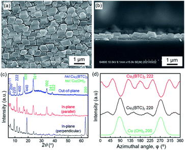 |
| | Fig. 1 SEM images ((a) top view and (b) cross-section) of the oriented Cu3(BTC)2 thin film (the longitudinal direction (a-axis) of the underlying Cu(OH)2 nanobelts is aligned horizontal to the images). (c) XRD patterns of the oriented Cu3(BTC)2 thin film. Three setups for the XRD investigations were used: out-of-plane (blue line), in-plane (red and black line; X-ray incident angle is parallel, and perpendicular to longitudinal direction of nanobelts at φ = 0°). (d) Azimuthal angle dependence of intensity (φ scan) profiles of the 222 and 220 reflections of Cu3(BTC)2 and 200 reflection of Cu(OH)2 (X-ray incident angle is parallel to longitudinal direction (a-axis) of Cu(OH)2 nanobelts at φ = 0°). | |
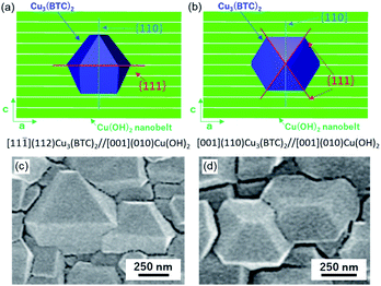 |
| | Fig. 2 Schematics and SEM images of the Cu3(BTC)2 crystals epitaxially grown under [11](112)Cu3(BTC)2//[001](010)Cu(OH)2 (a and c) and [001](110)Cu3(BTC)2//[001](010)Cu(OH)2 (b and d) orientation relationships. The cuboctahedron-shaped crystals and green rectangles denote the Cu3(BTC)2 crystals and Cu(OH)2 nanobelts, respectively. In the SEM images, the longitudinal direction (a-axis) of the underlying Cu(OH)2 nanobelts is aligned horizontal to the images. | |
The orientation of Cu3(BTC)2 can be explained by the epitaxial growth on Cu(OH)2. As revealed by the XRD investigation, Cu3(BTC)2 crystals epitaxially grow under two different types of orientation relationships: [11](112)Cu3(BTC)2//[001](010)Cu(OH)2 and [001](110)Cu3(BTC)2//[001](010)Cu(OH)2. The key to the epitaxial growth of Cu3(BTC)2 in the orientation relationships is the interface bonding (local chemical connection matching; spatial matching of Cu atoms across the Cu3(BTC)2/Cu(OH)2 interface). If only the lattice mismatch is considered, then better orientation relationships (e.g. [010](100)Cu3(BTC)2//[001](010)Cu(OH)2 with 0.68%) are obtained; however, these orientations were not confirmed. It is important to note that, in the two different types of orientation relationships observed in the present work, the Cu–Cu in the Cu-paddlewheel units in Cu3(BTC)2 is parallel to a-axis of Cu(OH)2 at the interface (see Fig. S6 and S7†). The Cu–Cu distance of the Cu-paddlewheel units in Cu3(BTC)2 is approximately 2.63 Å, which is in good agreement with the distance between Cu atoms along the a-axis of Cu(OH)2 (2.95 Å). This allows the formation of coordination bonds between Cu(OH)2 and the carboxylic acid of the BTC linker at the Cu3(BTC)2/Cu(OH)2 interface. Other orientation relationships are unsuitable for forming coordination bonds with the carboxylic acid owing to the large distances between Cu atoms. The bond formation requirement at the interface results in the alignment of Cu-paddlewheel units parallel to the a-axis of Cu(OH)2. In both orientation relationships, the lattice mismatch was sufficiently small for epitaxial growth: 5.34% for [11](112)Cu3(BTC)2//[001](010)Cu(OH)2 and 5.34% for [001](110)Cu3(BTC)2//[001](010)Cu(OH)2. Both lattice matching at the interface and interface bonding were found to be important for the epitaxial growth of MOFs. The epitaxial growth conditions of MOFs, considering both lattice matching at the interface and interface bonding, have recently been considered in the field of MOF epitaxial growth, such as single crystal MOF-on-MOF systems, and our computational study on the epitaxial growth of Cu-based MOFs on Cu(OH)2.31,32
2.2 Oriented Cu3(BTC)2 patterns
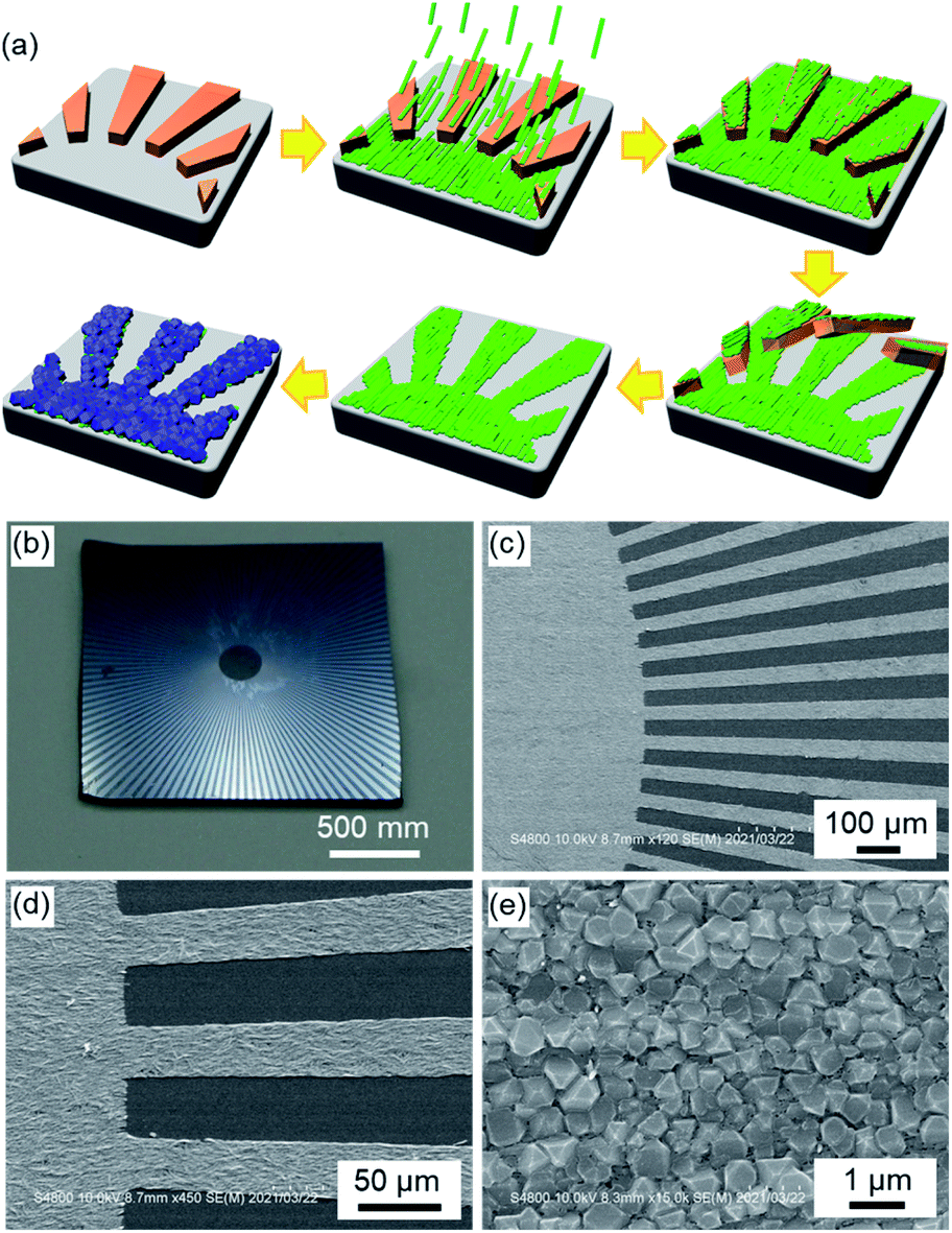
The development of a novel method to precisely control both the crystallographic orientation of MOFs and the MOF position on substrates is a fundamental step towards exploiting the unique properties of MOFs in miniaturised devices, such as lab-on-a-chip or microfluidic devices.33 Among the different approaches (e.g. the use of pre-patterned SAM), the fabrication of MOF patterns by photolithography used in current microfabrication technology is a promising method because of the formation of high-resolution MOF patterns and compatibility with existing semiconductor fabrication processes.18,34–37 Although photolithography techniques can efficiently prepare precise MOF patterns, the fabrication of MOF patterns with crystallographic orientation (oriented MOF patterns) by integration with conventional lithography technology remains a challenge. In particular, the oriented MOF patterns of semiconducting TCNQ@Cu3(BTC)2 contribute to the development of MOF-based thin-film devices. The present approach, which uses Cu(OH)2 nanoassemblies as a support for MOF growth, offers advantages in terms of the MOF orientation and the formation of MOF thin films and patterns on various substrates.38–40 Here, we show for the first time the fabrication of oriented MOF patterns with micrometre-scale resolution in combination with conventional photolithography techniques (Fig. 3). Fabrication was conducted using the following process. The photoresist patterns were fabricated on a Si wafer using a standard UV lithography method. The oriented Cu(OH)2 thin film was deposited onto the Si wafer with the photoresist patterns. The photoresist patterns were then removed by ultrasonic treatment in acetone. The resulting oriented Cu(OH)2 patterns were converted into oriented Cu3(BTC)2 patterns. The orientation of the Cu3(BTC)2 patterns was confirmed by XRD (see Fig. S8†). No pattern detachment was observed during the conversion process. Oriented MOF patterns that finely transferred the photomask patterns were obtained. By using a higher resolution photoresist pattern, it will be possible to form an oriented MOF pattern with a higher resolution. As the width of the Cu(OH)2 nanobelt is approximately 50 nm, the fabrication of oriented MOF patterns with a resolution of up to 50 nm is possible by combination with recently developed microfabrication technology.
 |
| | Fig. 3 Fabrication of oriented Cu3(BTC)2 MOF patterns. (a) Schematics showing the fabrication process. The photoresist patterns (orange blocks) were fabricated on the Si wafer using a standard UV lithography method. The Cu(OH)2 (green rectangles) oriented thin film was deposited onto the Si wafer with the photoresist patterns. The photoresist patterns on which Cu(OH)2 was deposited were removed by ultrasonic treatment in acetone. The resulting oriented Cu(OH)2 patterns were converted into oriented Cu3(BTC)2 (blue cuboctahedron-shaped crystal) patterns. (b–e) Photo and SEM images of the oriented Cu3(BTC)2 patterns. In this film, the longitudinal direction (a-axis) of the underlying Cu(OH)2 nanobelts is aligned horizontal to the images. | |
2.3 Anisotropic conductivity of the oriented TCNQ@Cu3(BTC)2 film
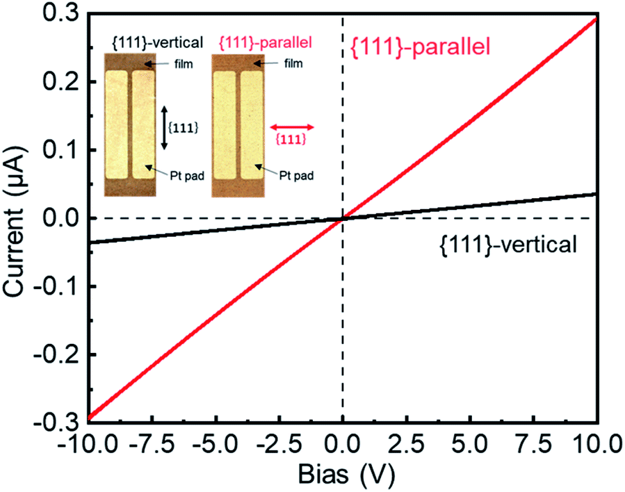
The electrical conductivity of oriented Cu3(BTC)2 thin films infiltrated with TCNQ was investigated (Fig. 4 and see Fig. S9†). The infiltration of TCNQ into the oriented Cu3(BTC)2 thin film was conducted as follows. First, the oriented Cu3(BTC)2 thin film prepared on polyimide was placed in a borosilicate glass tube and desolvated under high vacuum (∼10−4 Pa) at 180 °C for 3 h. The film was removed from the borosilicate glass tube, placed in a glove bag filled with N2 gas, and immersed in a saturated TCNQ solution in dichloromethane for three days. After three days, the TCNQ@Cu3(BTC)2 was washed twice with dichloromethane and then air-dried. By changing the orientation of the underlying Cu(OH)2 nanobelts on the substrate, the directional relationship between the {111} lattice planes of TCNQ@Cu3(BTC)2 and the direction of electrical measurements (position of the Pt electrodes) can be defined. The conductivity in the direction parallel and vertical to the {111} lattice planes of TCNQ@Cu3(BTC)2 were compared by a two-probe method. Electrical measurements showed that the thin film exhibited ohmic behaviour. Its electrical conductivity was approximately 10 times higher in the direction parallel to the {111} lattice planes (∼3.2 × 10⁻³ S m−1) compared with the direction perpendicular to the {111} lattice planes (∼3.9 × 10⁻⁴ S m−1). The underlying Cu(OH)2 nanobelt film showed 1000 times lower conductivity than the TCNQ@Cu3(BTC)2 thin film (Fig. S10†), indicating that the anisotropic conductivity is attributed to TCNQ@Cu3(BTC)2. TCNQ molecules are known to preferentially align along the {111} lattice planes of Cu3(BTC)2 MOFs by bridging the coordination motif to two neighbouring Cu-paddlewheels (see Fig. S11†).13,17 Thus, the oriented TCNQ@Cu3(BTC)2 film showed higher conductivity in the {111} direction. Although anisotropic electrical conductivity and exciton migration have been reported using single-crystal MOFs,41,42 these results show, for the first time, the anisotropic conductivity in the in-plane direction over a large area of polycrystalline MOF thin films. The anisotropic conductivity of the thin film is attributed to the angular dependence of the {111} lattice planes, which is the conducting path of TCNQ@Cu3(BTC)2 in the in-plane direction.
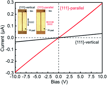 |
| | Fig. 4
I–V curves of the oriented TCNQ@Cu3(BTC)2 thin films on polyimide substrates (Pt pads were 100 μm apart from each other). Electrical measurements were carried out parallel to the {111} lattice plane ({111}-parallel) and vertical to the {111} lattice plane ({111}-vertical). | |
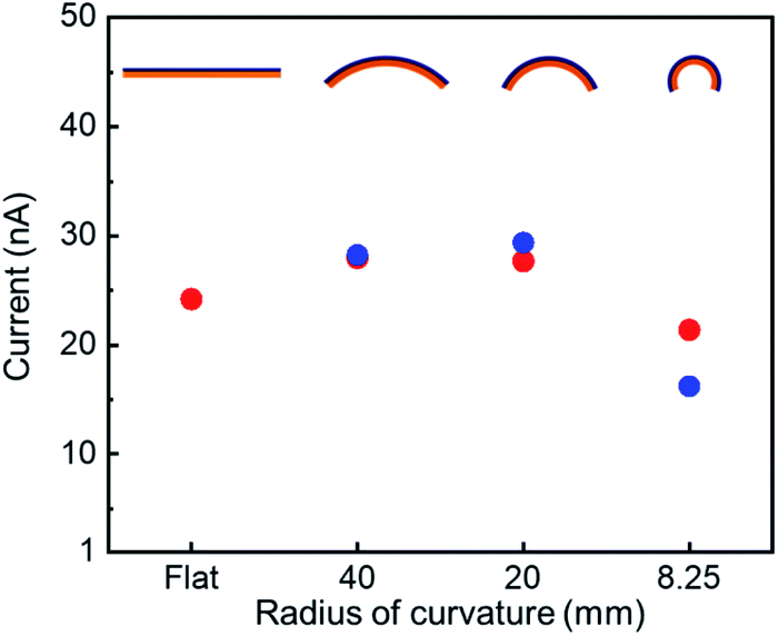
The effect of substrate bending on the electrical properties of the oriented TCNQ@Cu3(BTC)2 thin film was also investigated (Fig. 5). The oriented TCNQ@Cu3(BTC)2 thin film prepared on an elastic polyimide substrate was bent until the radius of curvature reached 8.25 mm. However, because of the polycrystalline nature of the thin film, the conductivity did not change significantly from when it was flat. No obvious change was observed between the bending of the substrate perpendicular to the longitudinal direction (a-axis) of the underlying Cu(OH)2 nanobelts and the bending of the substrate perpendicular to the short direction (c-axis) of the underlying Cu(OH)2 nanobelts. This small difference can be attributed to the anisotropic structure of the underlying Cu(OH)2 nanobelts; the flexible Cu(OH)2 nanobelt film against bending of the substrate parallel to the longitudinal direction prevented crack formation in the TCNQ@Cu3(BTC)2 thin film. The fabrication of flexible MOF-based thin films with electrical properties is attributed to the flexibility of the organic–inorganic hybrid material MOFs and the flexible deformation of thin films consisting of Cu(OH)2 nano-assemblies and TCNQ@Cu3(BTC)2 crystallites against macroscopic structural deformation. Flexible and conductive thin films are more feasible for realistic applications in industry than single crystals. The present method, which does not require a specific substrate (e.g. SAM-modified substrate) for the fabrication of oriented TCNQ@Cu3(BTC)2 thin films, allows for substrate versatility and the formation of semiconducting TCNQ@Cu3(BTC)2 thin films on flexible substrates. These advantages enabled us to show, for the first time, the effect of substrate bending on the electrical properties of TCNQ@Cu3(BTC)2 thin films. This will contribute to the research and development of MOF-based (flexible) thin-film smart device applications, such as transistors and thermoelectric thin films.
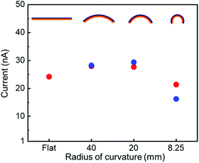 |
| | Fig. 5 Current as a function of bending radius of curvature at 10 V (blue circles: bending of a substrate perpendicular to the longitudinal direction (a-axis) of the underlying Cu(OH)2 nanobelts. Red circles: bending of a substrate perpendicular to the short direction (c-axis) of the underlying Cu(OH)2 nanobelts). | |
3. Conclusions
Three-dimensionally (both in-plane and out-of-plane directions) oriented Cu3(BTC)2 thin films over a large centimetre-scale area were synthesised via epitaxial growth on Cu(OH)2. The epitaxial growth approach enables the fabrication of oriented TCNQ@Cu3(BTC)2 thin films, where the {111} lattice plane, which can be a conducting path, is oriented both parallel and perpendicular to the substrate. The Cu3(BTC)2 crystals were epitaxially grown with two types of orientation relationships: Cu3(BTC)2 epitaxially grown with either the {111} or {100} lattice planes parallel to the a-axis of Cu(OH)2. The orientation relationships were determined not only by the lattice matching between Cu3(BTC)2 and Cu(OH)2, but also by interface bonding (local chemical connection matching; spatial matching of Cu atoms across the interface). The realization of polycrystalline TCNQ@Cu3(BTC)2 thin films with in-plane orientation enables the fabrication of MOF-based thin films with anisotropic electrical properties in the in-plane direction. By combining the epitaxial growth approach on Cu(OH)2 nano-assemblies with UV lithography technology, the fabrication of oriented Cu3(BTC)2 patterns is possible. These semiconducting MOF films and patterns with anisotropic properties will pave the way for next-generation smart electronic devices.
Conflicts of interest
There are no conflicts to declare.
Acknowledgements
The present work is partially supported by grand-in-aids from the Ministry of Education, Culture, Sports, Science and Technology (MEXT), administrated by Japan Society for the Promotion of Science (JSPS), and also by JST, PRESTO Grant Number JPMJPR19I3, Japan. K. O. acknowledges financial support from Izumi Science and Technology Foundation.
Notes and references
- H. Furukawa, K. E. Cordova, M. O'Keeffe and O. M. Yaghi, Science, 2013, 341, 1230444 Search PubMed.
- S. Kitagawa, R. Kitaura and S.-I. Noro, Angew. Chem., Int. Ed., 2004, 43, 2334–2375 Search PubMed.
- J. Lee, O. K. Farha, J. Roberts, K. A. Scheidt, S. T. Nguyen and J. T. Hupp, Chem. Soc. Rev., 2009, 38, 1450–1459 Search PubMed.
- D. Yang and B. C. Gates, ACS Catal., 2019, 9, 1779–1798 Search PubMed.
- K. Adil, Y. Belmabkhout, R. S. Pillai, A. Cadiau, P. M. Bhatt, A. H. Assen, G. Maurin and M. Eddaoudi, Chem. Soc. Rev., 2017, 46, 3402–3430 Search PubMed.
- K. Sumida, D. L. Rogow, J. A. Mason, T. M. Mcdonald, E. D. Bloch, Z. R. Herm, T.-H. Bae and J. R. Long, Chem. Rev., 2012, 112, 724–781 Search PubMed.
- I. Stassen, N. Burtch, A. Talin, P. Falcaro, M. Allendorf and R. Ameloot, Chem. Soc. Rev., 2017, 46, 3185–3241 Search PubMed.
- L. S. Xie, G. Skorupskii and M. Dincă, Chem. Rev., 2020, 120, 8536–8580 Search PubMed.
- L. Sun, M. G. Campbell and M. Dincă, Angew. Chem., Int. Ed., 2016, 55, 3566–3579 Search PubMed.
- C. A. Downes and S. C. Marinescu, ChemSusChem, 2017, 10, 4374–4392 Search PubMed.
- G. Givaja, P. Amo-Ochoa, C. J. Gómez-García and F. Zamora, Chem. Soc. Rev., 2012, 41, 115–147 Search PubMed.
- L. Sun, S. S. Park, D. Sheberla and M. Dincă, J. Am. Chem. Soc., 2016, 138, 14772–14782 Search PubMed.
- A. A. Talin, A. Centrone, A. C. Ford, M. E. Foster, V. Stavila, P. Haney, R. A. Kinney, V. Szalai, F. El Gabaly, H. P. Yoon, F. Léonard and M. D. Allendorf, Science, 2014, 343, 66–69 Search PubMed.
- Z. Wang, D. Nminibapiel, P. Shrestha, J. Liu, W. Guo, P. G. Weidler, H. Baumgart, C. Wöll and E. Redel, ChemNanoMat, 2016, 2, 67–73 Search PubMed.
- X. Chen, Z. Wang, Z. M. Hassan, P. Lin, K. Zhang, H. Baumgart and E. Redel, ECS J. Solid State Sci. Technol., 2017, 6, 150–153 Search PubMed.
- K. J. Erickson, F. Léonard, V. Stavila, M. E. Foster, C. D. Spataru, R. E. Jones, B. M. Foley, P. E. Hopkins, M. D. Allendorf and A. A. Talin, Adv. Mater., 2015, 27, 3453–3459 Search PubMed.
- C. Schneider, D. Ukaj, R. Koerver, A. A. Talin, G. Kieslich, S. P. Pujari, H. Zuilhof, J. Janek, M. D. Allendorf and R. A. Fischer, Chem. Sci., 2018, 9, 7405–7412 Search PubMed.
- O. Shekhah, H. Wang, D. Zacher, R. A. Fischer and C. Wöll, Angew. Chem., Int. Ed., 2009, 48, 5038–5041 Search PubMed.
- O. Shekhah, H. Wang, S. Kowarik, F. Schreiber, M. Paulus, M. Tolan, C. Sternemann, F. Evers, D. Zacher, R. A. Fischer and C. Wöll, J. Am. Chem. Soc., 2007, 129, 15118–15119 Search PubMed.
- A. Schoedel, C. Scherb and T. Bein, Angew. Chem., Int. Ed., 2010, 49, 7225–7228 Search PubMed.
- H. K. Arslan, O. Shekhah, J. Wohlgemuth, M. Franzreb, R. A. Fischer and C. Wöll, Adv. Funct. Mater., 2011, 21, 4228–4231 Search PubMed.
- V. Stavila, J. Volponi, A. M. Katzenmeyer, M. C. Dixon and M. D. Allendorf, Chem. Sci., 2012, 3, 1531 Search PubMed.
- K. Thürmer, C. Schneider, V. Stavila, R. W. Friddle, F. Léonard, R. A. Fischer, M. D. Allendorf and A. A. Talin, ACS Appl. Mater. Interfaces, 2018, 10, 39400–39410 Search PubMed.
- F. Cheng, A. J. Young, J.-S. G. Bouillard, N. T. Kemp, R. Guillet-Nicolas, C. H. Hall, D. Roberts, A. H. Jaafar, A. M. Adawi, F. Kleitz, A. Imhof, M. R. Reithofer and J. M. Chin, J. Am. Chem. Soc., 2019, 141, 12989–12993 Search PubMed.
- K. Ikigaki, K. Okada, Y. Tokudome, T. Toyao, P. Falcaro, C. J. Doonan and M. Takahashi, Angew. Chem., Int. Ed., 2019, 58, 6886–6890 Search PubMed.
- K. Ikigaki, K. Okada, Y. Tokudome and M. Takahashi, J. Sol-Gel Sci. Technol., 2019, 89, 128–134 Search PubMed.
- P. Falcaro, K. Okada, T. Hara, K. Ikigaki, Y. Tokudome, A. W. Thornton, A. J. Hill, T. Williams, C. Doonan and M. Takahashi, Nat. Mater., 2017, 16, 342–348 Search PubMed.
- K. Ikigaki, K. Okada and M. Takahashi, ACS Appl. Nano Mater., 2021, 4, 3467–3475 Search PubMed.
- K. Okada, M. Nakanishi, K. Ikigaki, Y. Tokudome, P. Falcaro, C. J. Doonan and M. Takahashi, Chem. Sci., 2020, 11, 8005–8012 Search PubMed.
- Q. Liu, J.-M. Yang, L.-N. Jin and W.-Y. Sun, CrystEngComm, 2016, 18, 4127–4132 Search PubMed.
- O. Kwon, J. Y. Kim, S. Park, J. H. Lee, J. Ha, H. Park, H. R. Moon and J. Kim, Nat. Commun., 2019, 10, 3620 Search PubMed.
- A. Tarzia, M. Takahashi, P. Falcaro, A. W. Thornton, C. J. Doonan and D. M. Huang, ACS Appl. Mater. Interfaces, 2018, 10, 40938–40950 Search PubMed.
- P. Falcaro, D. Buso, A. J. Hill and C. M. Doherty, Adv. Mater., 2012, 24, 3153–3168 Search PubMed.
- M. Tu, B. Xia, D. E. Kravchenko, M. L. Tietze, A. J. Cruz, I. Stassen, T. Hauffman, J. Teyssandier, S. De Feyter, Z. Wang, R. A. Fischer, B. Marmiroli, H. Amenitsch, A. Torvisco, M. D. J. Velásquez-Hernández, P. Falcaro and R. Ameloot, Nat. Mater., 2021, 20, 93–99 Search PubMed.
- P. Falcaro, A. J. Hill, K. M. Nairn, J. Jasieniak, J. I. Mardel, T. J. Bastow, S. C. Mayo, M. Gimona, D. Gomez, H. J. Whitfield, R. Riccò, A. Patelli, B. Marmiroli, H. Amenitsch, T. Colson, L. Villanova and D. Buso, Nat. Commun., 2011, 2, 237 Search PubMed.
- S. Hermes, F. Schröder, R. Chelmowski, C. Wöll and R. A. Fischer, J. Am. Chem. Soc., 2005, 127, 13744–13745 Search PubMed.
- C. M. Doherty, G. Grenci, R. Riccò, J. I. Mardel, J. Reboul, S. Furukawa, S. Kitagawa, A. J. Hill and P. Falcaro, Adv. Mater., 2013, 25, 4701–4705 Search PubMed.
- K. Okada, S. Sawai, K. Ikigaki, Y. Tokudome, P. Falcaro and M. Takahashi, CrystEngComm, 2017, 19, 4194–4200 Search PubMed.
- T. Toyao, K. Liang, K. Okada, R. Ricco, M. J. Styles, Y. Tokudome, Y. Horiuchi, A. J. Hill, M. Takahashi, M. Matsuoka and P. Falcaro, Inorg. Chem. Front., 2015, 2, 434–441 Search PubMed.
- K. Okada, R. Ricco, Y. Tokudome, M. J. Styles, A. J. Hill, M. Takahashi and P. Falcaro, Adv. Funct. Mater., 2014, 24, 1969–1977 Search PubMed.
- H.-J. Son, S. Jin, S. Patwardhan, S. J. Wezenberg, N. C. Jeong, M. So, C. E. Wilmer, A. A. Sarjeant, G. C. Schatz, R. Q. Snurr, O. K. Farha, G. P. Wiederrecht and J. T. Hupp, J. Am. Chem. Soc., 2013, 135, 862–869 Search PubMed.
- J.-H. Dou, M. Q. Arguilla, Y. Luo, J. Li, W. Zhang, L. Sun, J. L. Mancuso, L. Yang, T. Chen, L. R. Parent, G. Skorupskii, N. J. Libretto, C. Sun, M. C. Yang, P. V. Dip, E. J. Brignole, J. T. Miller, J. Kong, C. H. Hendon, J. Sun and M. Dincă, Nat. Mater., 2021, 20, 222–228 Search PubMed.
Footnote |
| † Electronic supplementary information (ESI) available. See DOI: 10.1039/d1ta02968a |
|
| This journal is © The Royal Society of Chemistry 2021 |
Click here to see how this site uses Cookies. View our privacy policy here. 
 Open Access Article
 This Open Access Article is licensed under a Creative Commons Attribution-Non Commercial 3.0 Unported Licence
 *ab,
Keyaki
Mori
a,
Arisa
Fukatsu
*ab,
Keyaki
Mori
a,
Arisa
Fukatsu