
 Open Access Article
 This Open Access Article is licensed under a Creative Commons Attribution-Non Commercial 3.0 Unported Licence
Open-air, low-temperature deposition of phase pure Cu2O thin films as efficient hole-transporting layers for silicon heterojunction solar cells†
Van Son
Nguyen‡
a,
Abderrahime
Sekkat‡
 bcd,
Daniel
Bellet
b,
Guy
Chichignoud
d,
Anne
Kaminski-Cachopo
c,
David
Muñoz-Rojas
*b and
Wilfried
Favre
*a
bcd,
Daniel
Bellet
b,
Guy
Chichignoud
d,
Anne
Kaminski-Cachopo
c,
David
Muñoz-Rojas
*b and
Wilfried
Favre
*a
aUniv. Grenoble Alpes, CEA, LITEN, DTS, LPH, INES, F-38000 Grenoble, France
bUniv. Grenoble Alpes, CNRS, Grenoble INP, LMGP, 38000 Grenoble, France. E-mail: david.munoz-rojas@grenoble-inp.fr
cUniv. Grenoble Alpes, Univ. Savoie Mont Blanc, CNRS, Grenoble INP, IMEP-LaHC, 38000 Grenoble, France
dUniv. Grenoble Alpes, CNRS, Grenoble INP, SIMAP, 38000 Grenoble, France
First published on 5th July 2021
Abstract
Recent research focuses on finding alternative materials and fabrication techniques to replace traditional (p) and (n) doped hydrogenated amorphous silicon (a-Si:H) to reduce cost and boost the efficiency of silicon heterojunction (SHJ) solar cells. In this work, low-cost p-type Cu2O thin films have been investigated and integrated as a hole-transporting layer (HTL) in SHJ solar cells, using atmospheric-pressure spatial atomic layer deposition (AP-SALD), an open-air, scalable ALD approach. Phase pure Cu2O thin films have been deposited at temperatures below the degradation limit of the SHJ, thus maintaining the passivation effect of the a-Si:H layer. The effect of deposition temperatures and HTL thicknesses on the performance of the devices has been evaluated. The fabricated Cu2O HTL-based SHJ cells, having an area of 9 cm2, reach a power conversion efficiency (PCE) of 13.7%, which is the highest reported efficiency for silicon-based solar cells incorporating a Cu2O HTL.
SHJ solar cells combining thin hydrogenated amorphous silicon (a-Si:H) layers with a crystalline silicon (c-Si) absorber are a mature technology that has demonstrated record efficiencies above 25% for large-area devices (∼180 cm2), both using the interdigitated back contact (IBC) or both sides contacted (BSC) architectures.1–5 The use of a-Si:H layers between the crystalline silicon core and the metal contact promotes a drastic reduction of recombination at the contacts, yielding an increase in the open-circuit voltage.3,6 The doped thin a-Si:H layers act both as a passivation film on the dangling bonds of the crystalline silicon wafer and as a selective contact. This is mainly attributed to the high hydrogen content and ability to promote doping of these films, together with adequate interface band offsets.5,7,8 Such passivation effect allows to use thinner c-Si wafers, and thus, this technology represents a promising alternative to the current c-Si technology.9
Due to their wider bandgap (∼1.7 eV) with respect to crystalline silicon, a-Si:H films offer higher transparency, thus facilitating the transmission of photons to the bulk absorber.10–12 Nevertheless, the transparency of these films is still not enough to avoid parasitic absorption at the front side of the device.13–15 Another major drawback of the a-Si:H layers is their low conductivity, which therefore increases the series resistance within the device.16,17 As an alternative, several works focus on the development of nano-crystalline layers (nc-SiOx:H) to substitute the a-Si:H layer, to improve both the conductivity and the transparency of this active window layer.18–21
In a different approach, several groups have proposed to replace the a-Si:H films by oxides or alkaline metals,7,22–24 targeting ultra-low surface recombination velocities, high transparency, excellent carrier selectivity and low resistivity values.22 Among the different oxides, Cu2O is a promising semi-transparent p-type HTL thanks to the high abundance of Cu, a work function of 5 eV (close to ∼5.2 eV of a-Si:H(p)), and a wide optical bandgap of approximately 2.1 eV.25 As a result, Cu2O has been explored as a component in numerous optoelectronic applications, such as photovoltaics,26–28 water splitting,29,30 and photodetectors.31–33
The integration of Cu2O in emerging and industrial-scale solar cell technologies has shown strong interest in recent years:34 it has been integrated into hybrid perovskite solar cells as a HTL and buffer layer, contributing both to the enhancement of the power conversion efficiency and the stability of the perovskite films.35–37 In organic solar devices, Cu2O has demonstrated an improvement in the power conversion efficiency compared to conventional PEDOT:PSS HTL.38 Cu2O is also being heavily explored as potential component in Si based PV technologies. Undoped and doped sputtered Cu2O has been explored for the first time as a hole selective contact in c-Si solar cells.39 The maximum reached power conversion efficiency reached so far for Si based solar cells is 9.54%, incorporating a solution-processed Cu2O layer and after introducing MoOx antireflective coating.40
Cu2O is also potential candidate to replace the a-Si:H(p) layer in SHJ devices due to its high conductivity, matched energy level, and high mobility value.34,41 But Cu2O HTLs developed so far in the literature are mostly obtained with growth techniques that require either high thermal budgets (>350 °C) or involving several steps. These growth conditions are incompatible with SHJ cells, which require low-temperature processing to preserve the passivation conferred by the a-Si:H. Apart from being able to deposit the Cu2O layers at maximum temperatures around 200 °C, their implementation in SHJ cells also requires low-cost and scalable processing while retaining good transport properties and high growth rate. Atmospheric pressure-spatial atomic layer deposition (AP-SALD) represents an appealing option since it allows the deposition of high-quality thin films at low temperatures and high throughout,42 even when processing at atmospheric pressure.43 AP-SALD has indeed already been widely applied to new generation photovoltaic technologies,44 among others.45–47 In particular, Cu2O thin films deposited by SALD have been extensively studied in terms of structural, optical, and electrical properties previously,48,49 and have been used in all-oxide ZnO/Cu2O solar cells.50
In this work, we have used AP-SALD to integrate Cu2O layers as HTL in 3 × 3 cm2 SHJ solar cells (see ESI and Fig. SI1† for details on the deposition system and parameters used and for details on the fabrication of the SHJ cells). The effect of the HTL deposition temperature and thickness on the passivation, recombination level, and output results after each step of the solar cell fabrication has been evaluated. Moreover, the obtained results are rationalised by performing a fitting two-diode model on the IV curves. Our cells present record efficiencies when compared to other Si-based solar cells incorporating Cu2O layers. Especially appealing is the large area for which our results have been obtained.
Fig. 1a shows the structure of SHJ cells incorporating Cu2O HTL layers. Similarly to the reference SHJ devices, the front side ITO transparent electrode enables carrier collection and improved conduction to the metallic electrodes.51 Besides, it also acts as an anti-reflective layer.22 A cross-section SEM picture also illustrating the bottom part of the cell is also included, where the Cu2O is clearly observed. Fig. 1b and c show optical images of the bare device rear side (with no ITO/Ag contacts), without and with a 200 nm thick Cu2O layer on top of the textured silicon surface. The figure also shows the corresponding tilted cross-section SEM views. The Cu2O layer is conformal over the textured Si surface (pyramids) and appears continuous and free of pinholes, which is a prerequisite to minimize shunt-related defects.
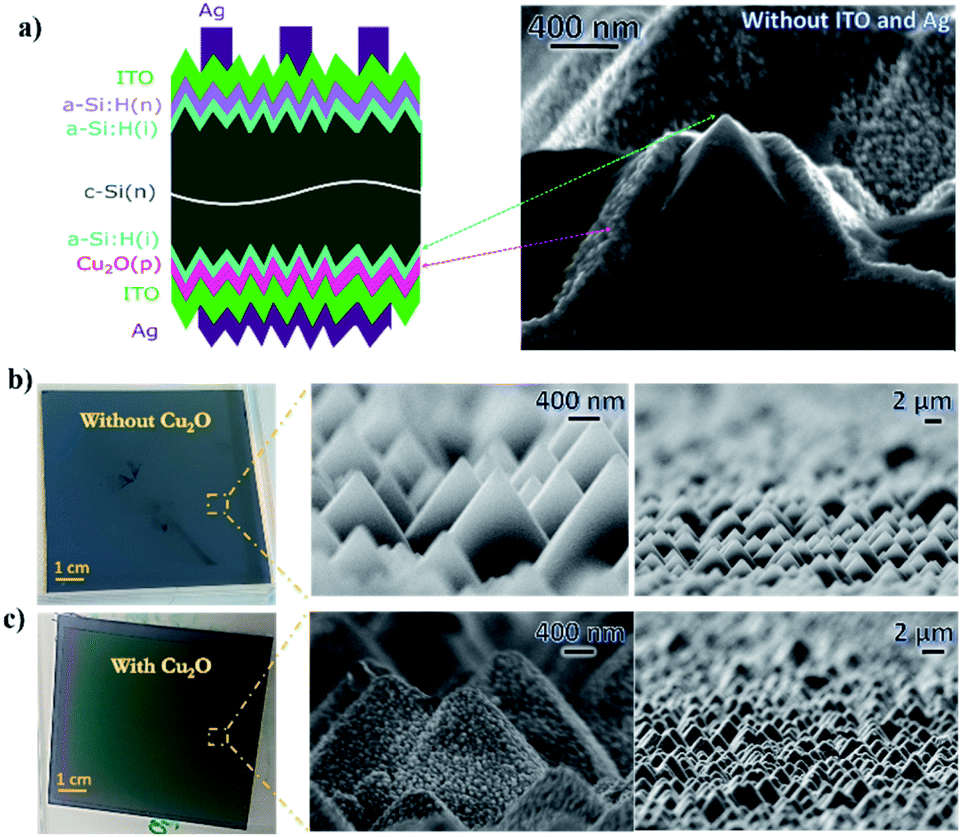 | ||
| Fig. 1 (a) Schematic diagram of Cu2O HTL based solar cells and a cross-section SEM of Cu2O film on top of textured silicon surface without ITO and Ag contacts. (b) Optical (left) and SEM (middle and right) images of bare a-Si:H(i) without Cu2O thin film deposited on top of textured SHJ with a cross section zoom over the rear bare Si side. (c) Optical and SEM images of the SHJ architecture with a zoom over rear side of the coated 200 nm Cu2O HTL on Si pyramids and the front side of SHJ. | ||
In our study, 10 nm, 60 nm, and 80 nm thick Cu2O films were deposited either at 200 °C or 220 °C. Raman spectroscopy indicates no presence of other phases (CuO and/or Cu), as shown in Fig. 2a. The intensity of the peaks observed is mostly the result of film thickness. Further study on that aspect was performed using X-ray diffraction (XRD) measurements for samples with a thickness of 80, 60, and 10 nm, as shown in Fig. 2b. The samples were titled during the measurement by 3° to diminish the effect of the silicon signal and the cuprous oxide on top is observed to be crystalline in all cases, in agreement with Raman data, with a preferential texture orientation along the (111) plane, which corresponds to the reflection at 36.28° (referenced to the ICSD26963 database).52 The difference in peak intensity between the 80 nm and 60 nm films is mainly due to the different deposition temperature and resulting crystallinity.48 In the case of the 10 nm films, the low intensity is mainly due to the low thickness of the film (XPS was also performed to rule out the presence of traces of CuO or Cu in the film. The results confirm that the films only contain Cu2O, as shown in ESI Fig. SI2†). Fig. 2c and d shows the cross-section TEM analysis of the Cu2O deposited on top of the SHJ cells, for 10 nm and 60 nm thick Cu2O HTL. The images confirm that the films do not present cracks nor pinholes and that they follow the profile of the textured Si in a very conformal fashion.
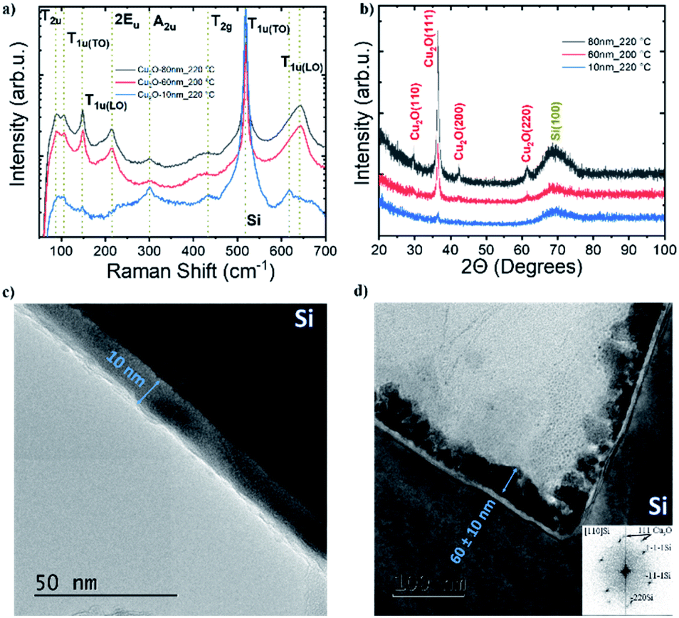 | ||
| Fig. 2 (a) Raman spectra of Cu2O thin films deposited at different temperatures on the SHJ cell, obtained with a 488 nm laser. The typically observed Raman modes for Cu2O are included as reference. (b) XRD pattern of 80 nm, 60 nm, and 10 nm thick Cu2O film deposited on top of the SHJCs at 220 °C and 200 °C, and cross-section TEM images of (c) the 10 nm (d) and 60 ± 10 nm thick Cu2O films. The inset in (d) shows a selected-area electron diffraction (SAED) pattern. | ||
One of the main concerns while integrating Cu2O HTL into SHJ cells is the passivation quality, which should be conserved after the deposition process to allow reaching a high open-circuit voltage (Voc). Fig. 3a and b show photoluminescence (PL) images of both standard cells with an a-Si:H(p) layer and cells with a 10 nm Cu2O HTL. PL data was obtained at different stages: before Cu2O deposition and after the deposition of ITO and the silver contact. PL intensity can be directly converted to the absolute excess minority carrier densities (MCDs).53 The Voc value is in turn related to the excess MCDs Δn and Δp (considering: Δp = Δn) by the equation:54 where Nd is the doping concentration, ni is the intrinsic carrier concentration, k the Boltzmann constant (≈8.617 × 10⁻⁵ eV K−1) and T is temperature (K). Therefore, an implied Voc can be quantitatively estimated from PL data. With the presence of Cu2O HTL, it appears that the PL intensity was lower at some local areas, indicating a lower excess MCD in these regions as a result of a higher recombination. In addition to PL measurements, carrier recombination has also been evaluated with a WTC120 instrument from Sinton. After the deposition of the Cu2O HTL, minority carrier lifetimes and the corresponding implied Voc at specific MCD = 1015 cm−3 were reduced from 2140 μs and 736 mV to 1156 μs and 729 mV, respectively, as shown in Fig. 3d. The values obtained for the reference cell with a-Si:H(p) and without ITO/Ag contact is equal, however, to 1858 μs and 733 mV respectively. Thus, it can be concluded that the SALD deposition did not degrade drastically the passivation properties during the growth of the 10 nm thick Cu2O film, since the implied-Voc stays almost the same with a reduction of the lifetime values. This is in agreement with previous reports on the deposition of ZnO layers by AP-SALD on SHJ cells.44 For thicker Cu2O layers, we found strong PL intensity reduction on the sample borders, in the regions covered by the hard mask (see Fig. SI3†). In addition, transportation and more handling of the samples was required for the SALD coating, which could have caused further damages on the cells incorporating the Cu2O HTL as compared with the standard cells.
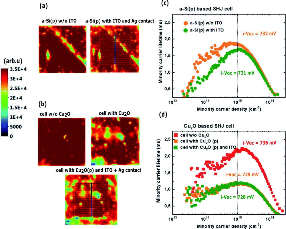 | ||
| Fig. 3 PL maps of (a) a-Si:H(p) HTL based SHJ cell: before/after the deposition of ITO and the Ag contacts, and (b) 10 nm Cu2O HTL based SHJ cell: before/after Cu2O and before/after the deposition of ITO and the Ag contacts; the scale bar represents the PL intensity in arbitrary units. The corresponding carrier lifetime measurements are followed at each stage of (c) a-Si:H(p) based and (d) Cu2O based SHJ cell. Minority carrier lifetime (MCL) of each measurement on 9 cm2 aperture area was taken at typical minority carrier density MCD = 1015 cm−3 (indicated by a dotted black line). The corresponding i-Vocs were also indicated. | ||
It can be seen from Fig. 3c that there is almost no lifetime value change after ITO deposition for the reference sample at MCD > 1015 cm−3, while it is reduced as MCD < 1015 cm−3, as often observed in the literature.55 Similarly, on Fig. 3d, we can observe that almost no further change in the lifetime measurements is observed after ITO deposition on top of the Cu2O HTL over the full MCD range. This could be related to the slight protection provided by the 10 nm (or thicker) Cu2O layer from ITO sputtering process damages.56 Even though the passivation quality of the Cu2O based SHJ cell is lower than the reference one, samples with τeff ≈ 1156 μs and implied i-Voc ≈ 729 mV still remain acceptable for SHJ cell finalization. Indeed, these values fall in the same order of magnitude of the a-Si:H(p) SHJ (only 4 mV lower), showing that replacing this latter layer by a Cu2O HTL does not affect significantly the passivation properties at the c-Si/a-Si:H(i) rear interface.
All the Cu2O HTL with different thickness were thus integrated into complete SHJ cells and the performances were evaluated. The IV curves and a table summarizing the obtained cell parameters are presented in Fig. 4a and b. In the best case, i.e. for the SHJ cell with a 10 nm thick Cu2O HTL, a Voc of 584 mV and a Jsc of 36.8 mA cm−2 could be obtained, leading to a maximum power conversion efficiency (PCE) obtained on the 9 cm2 inverted emitter prototype is 13.7%. EQE (external quantum efficiency) measurements were conducted on the best sample, as shown in Fig. 4c. The obtained EQE is very similar to the one obtained for the standard cell incorporating an a-Si:H(i) layer (Fig. SI4,† the IV of a standard cell is also included), especially in the infrared range where the replacement of a-Si:H(i) by Cu2O was expected to have more impact. The Jsc values calculated from the EQE data are 35.8 mA cm−2 and 36.4 mA cm−2 for the Cu2O and the a-Si:H(p) based cells, respectively. These values are in good agreement with the values obtained from the JV measurement. The small difference could be related to a slight variance of hard mask manual positioning when doing the different characterizations (note that the silver contacts accounts for 5.8% of the aperture area).
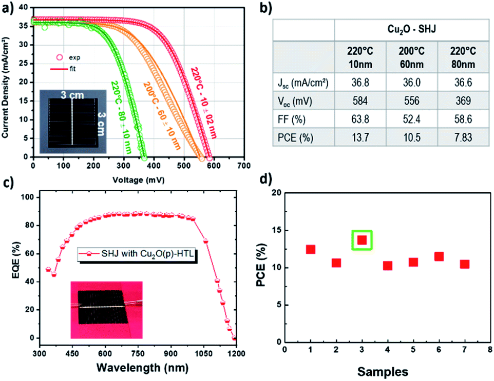 | ||
| Fig. 4 (a) J–V characteristics (measured under 1 sun) of SHJ cells integrating different Cu2O HTL and the corresponding fitting curves. Inset: picture of the 9 cm2 active cell. (b) Cell performances of the devices in (a). (c) EQE measurement (average over 3 successive measurements) of the SHJ cell incorporating a Cu2O HTL deposited at 220 °C with a 10 nm thickness. The inset depicts a picture of the cell during measurement. (d) PCE obtained for different samples. Values above 10% were obtained for all seven cells measured, with a best efficiency of 13.7% being obtained [green square]. Note that the front metal grid shadowing is estimated to 5.8% and could be further optimized for Jsc enhancement. | ||
A small difference in Jsc (∼0.5 mA) is observed between the two samples (Fig. SI4†) where EQE is slightly smaller at the green–blue range but may be related to poor signal to noise ratio for the very first acquisition point (340 nm). In addition, good surface passivation and moderately high carrier lifetime contributed to the Jsc in this rear emitter configuration. However, the Jsc can be still improved by reducing recombination and optimizing the front metal grid design to reduce shading with a potential gain of 0.8% shading reduction.
A limiting parameter for the efficiency is the fill factor (FF). The reported FF for our best device is 63.8%, which is comparable to 66.2% and 66.3%, reported for perovskite solar cells incorporating a Cu2O HTL,35,38 and is much higher than the maximum reported value of 40.6% for Cu2O HTL integrated into Si-based devices.39 However, this value is sensibly lower than the typical 78–84% generally reported for crystalline silicon based devices. Furthermore, the obtained fill factor value is mainly correlated to the large contribution of the series resistance between (i) a-Si:H(i)/Cu2O and/or Cu2O/ITO interfaces that could be decreased by optimizing further the growth conditions.
The influence of the Cu2O on deposition temperature on the performance of integrated SHJ devices was investigated. JV curves of samples with Cu2O deposited at different parameters are presented in Fig. 4a, and show that for lower deposition temperatures and thicker HTL layers, the performance of the cell is decreased. In order to rationalise these results, a two-diode model was used to fit the relation between the current J and voltage V57,58 (see the used equivalent circuit in Fig. SI5†):

The fitting data, displayed in Table 1, show that the diode saturation current densities as well as the ideality factors are in the same order of magnitude as reported for the two-diode model.58 This accounts for the high short-circuit current for all studied SHJ cells either with a-Si:H(p) or Cu2O HTL. It should be noted that the diode saturation current densities and shunt resistance vary very little from one sample to another.
| J–V fitting results | |||
|---|---|---|---|
| Cu2O temperature–thickness | 220 °C–10 nm | 200 °C–60 nm | 220 °C–80 nm |
| Temperature (T), K | 300 | 300 | 300 |
| Diode ideality factor (n1) | 1 | 1 | 1 |
| Diode ideality factor (n2) | 2.05 | 1.7 | 1.12 |
| Current density (J01), A cm−2 | 3.20 × 10⁻¹² | 3.00 × 10⁻¹² | 2.00 × 10⁻¹² |
| Current density (J02), A cm−2 | 1.90 × 10⁻⁷ | 9.00 × 10⁻⁶ | 1.00 × 10⁻⁷ |
| Shunt resistance (Rsh), Ω cm2 | 7.00 × 10⁴ | 8.00 × 10⁴ | 5.00 × 10⁴ |
| Serial resistance (Rs), Ω cm2 | 2.65 | 4 | 1.85 |
Interestingly, the cell with a 60 ± 10 nm thick Cu2O HTL deposited at 200 °C shows the highest series resistance. This is in agreement with an increase in resistivity of Cu2O thin films when decreasing the deposition temperature with AP-SALD.48,49 Therefore, we consider that series resistance is one of the main parameters limiting the cell performance. On the other hand, in some occasions the JV curve presents a small S-shape which possibly stems from the counter-diode effect where the interface ITO(n)/Cu2O(p) electrically acts as a parasitic p–n junction. In addition, it can be seen from the JV curve (Fig. 4a, green curve) that the last sample deposited at 220 °C together with a higher number of deposition cycles (80 nm) can degrade further the cell. The decrease of Voc (down to 369 mV) might result from a suppression in passivation due to longer AP-SALD deposition time. In the same line, it has indeed been shown that the short deposition times offered by AP-SALD have allowed to deposit buffer layer oxides, at temperatures up to 180 °C, on sensitive hybrid perovskite cells without degrading them.37,59
Our results represent the best efficiency value ever reported for a Si-based solar cell using Cu2O as a hole transporting or buffer layer. Indeed, several works have been reported on doped and undoped Cu2O being integrated in cells based on c-Si. Markose et al. have reported a sputtered boron-doped and undoped Cu2O as a hole-selective layer for c-Si solar cell.39 The maximum achieved power conversion efficiency was around 5.48% with a reported Voc of 114 mV for non-doped films and 370 mV for the doped ones.39 Cu2O thin films deposited by sputtering techniques have been widely reported in the literature as hole selective layer in c-Si solar cell structures with maximum efficiency values of 3.39%,60 and 1.12%.61 Other approaches have been used to grow Cu2O and integrate them in Si-based solar cells with a low reported value 0.45% for electro-deposition approaches.62 The highest reported efficiencies so far are 9.54% using spin-coating approach40 and 6.02% with the thermal oxidation process.63 In all cases, the surface areas in these studies varied from 0.01 to 1 cm2, thus between 9 and 900 times smaller than for the study presented here. The validation of high efficiency values for large laboratory cells is a key factor towards the large-scale integration of a technology into industrial processes.
Table 2 summarizes the cell parameters, including cell area, for all reported Si-based cells incorporating a Cu2O layer, along with our results while Fig. 5 focuses on the differences in terms of efficiency, Jsc and area for the different reports. To sum up, most of the other deposition techniques require a high thermal budget in the case of the thermally oxidized films or complex processes such as sputtering (more damages, vacuum required) and spin coating as well as electrochemical techniques that provide hardly uniform films over the surface substrate (therefore not suitable for up-scaling). Furthermore, the comparison show that the surface area of the Cu2O deposited by other techniques is always deposited at the laboratory scale with a smaller surface area (<1 cm2) which prevents the facile integration to the industrial level. In this work, the HTL layer was deposited over a large surface area of 9 cm2 and the resulting solar cell exhibit higher efficiency and current density compared to other Si-based structures. This demonstrates the potential of using the SALD technique to integrate Cu2O HTL p-type semiconductor for the solar cell devices in the industrial and roll-to-roll processes.
| Cell type | Deposition methods | V oc (mV) | J sc (mA cm−2) | FF (%) | PCE (%) | Area (cm2) | Ref. |
|---|---|---|---|---|---|---|---|
| a ED: electrodeposited, TE: thermal evaporation. | |||||||
| Cu2O/SHJ | SALD | 584 | 36.8 | 63.8 | 13.7 | 9.0 | This work |
| Cu2O/Si | Sputtering | 114 | 19.39 | 29.2 | 0.64 | 1.0 | 39 |
| Cu2O:B/Si | Sputtering | 290 | 33.60 | 40.1 | 3.9 | 1.0 | |
| Cu2O:B/SiOx/Si | Sputtering | 370 | 36.50 | 40.6 | 5.48 | 1.0 | |
| Cu2O/Si | Spincoating | 528 | 30.08 | 60.01 | 9.54 | — | 40 |
| Cu2O:Na/Si | ED | 480 | 2.20 | 47.0 | 0.45 | — | 64 |
| Cu2O/Si | TE | 490 | 28.60 | 42.85 | 6.02 | 0.1 | 63 |
| Cu2O/Si | Sputtering | 328 | 11.90 | 50.5 | 1.97 | 0.019 | 60 |
| Cu2O/SiO2/Si | Sputtering | 528 | 13.20 | 48.6 | 3.39 | 0.019 | 60 |
| Cu2O/Si | Sputtering | 420 | 7.80 | 44.0 | 1.12 | 1 | 61 |
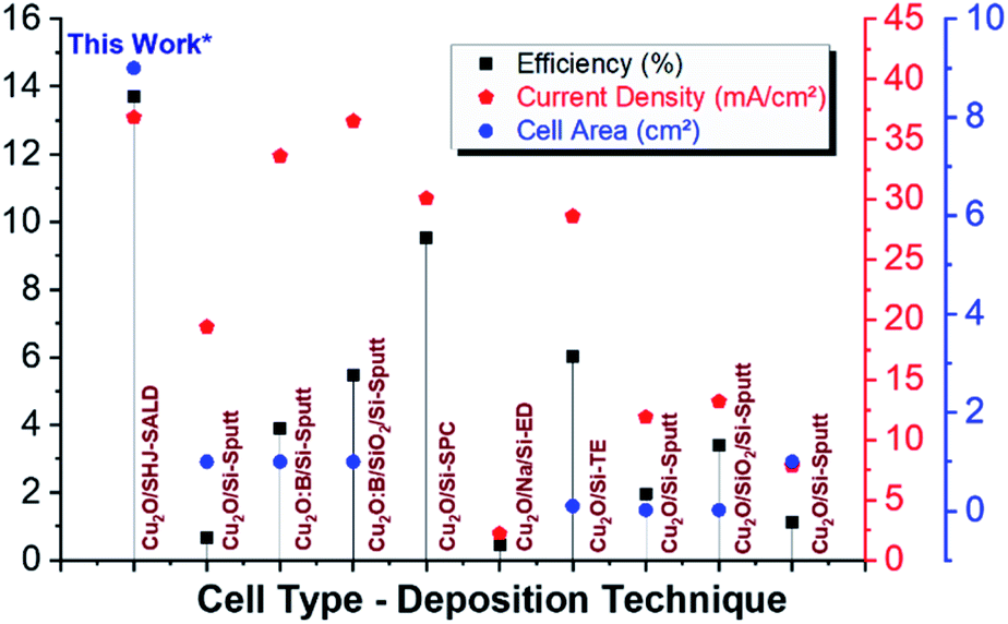 | ||
| Fig. 5 Comparative study of the area, efficiency, and current density of the SALD Cu2O/SHJ structure compared to SHJ in the literature. The compared deposition techniques are: Sputt: sputtering,39,60,61 SPC: spin coating,40 ED: electro-deposition,64 TE: thermally oxidized,63 SALD: spatial atomic layer deposition. | ||
Conclusions
In summary, we present the first rear emitter SHJ cell using Cu2O as a HTL, as a possible alternative to a-Si:H(p). AP-SALD was used to deposit the Cu2O HTL. Our results show that AP-SALD allows obtaining a conformal and uniform large area of Cu2O deposited at a low thermal budget without degrading the passivation effect of the a:Si:H(i) layer. The best efficiency obtained was 13.7% on a large-area 9 cm2 active cell, with a Jsc = 36.8 mA cm−2 and a Voc = 598 mV. These values were obtained for a 10 nm thick Cu2O HTL deposited at 220 °C and are the highest reported to our knowledge for PV devices integrating Cu2O as HTL in silicon absorber-based devices. These results could be related to the intrinsic high quality of SALD thin films, together with the low deposition temperature that prevents the degradation of the passivation properties at the c-Si/a-Si:H(i) rear interface. Further optimization in the deposition conditions and the corresponding transport properties of the Cu2O HTL are expected to increase further the efficiency of the device closer to that of standard SHJ. Finally, our work represents a proof-of-concept study of integrating Cu2O deposited by SALD as HTL in c-Si based PV devices.Conflicts of interest
There are no conflicts to declare.Acknowledgements
This work has been partially supported by the CDP Eco-SESA receiving funds from the French National Research Agency in the framework of the “Investments for the future” program (ANR-15-IDEX-02). The authors thank the Agence Nationale de la Recherche (ANR, France) via the projects DESPATCH (No. ANR-16-CE05-0021), OXYGENE (ANR-17-CE05-0034) and Carnot energies du future. D. M.-R acknowledges support from the European Union's Horizon 2020 FETOPEN-4191-2016-2017 research and innovation program under Grant Agreement 801464. D. M.-R. acknowledges funding through the Marie Curie Actions (FP7/2007-2013, Grant Agreement No. 63111). A. S. and D. M.-R. acknowledge the facilities, and the scientific and technical assistance of the CMTC characterization platform of Grenoble INP (Institute of Engineering) supported by the Centre of Excellence of Multifunctional Architectured Materials “CEMAM” n°ANR-10-LABX-44-01 funded by the “Investments for the Future” Program. The authors would like to thank CEA SHJ cell pilot line team for solar cells precursors preparation. The authors would like to thank Laetitia Rapenne for the TEM analysis and Dr João Resende and Dr Amal Chabli for fruitful discussions.Notes and references
- K. Yoshikawa, W. Yoshida, T. Irie, H. Kawasaki, K. Konishi, H. Ishibashi, T. Asatani, D. Adachi, M. Kanematsu, H. Uzu and K. Yamamoto, Sol. Energy Mater. Sol. Cells, 2017, 173, 37–42 CrossRef CAS.
- M. A. Green, Y. Hishikawa, E. D. Dunlop, D. H. Levi, J. Hohl-Ebinger and A. W. Y. Ho-Baillie, Prog. Photovoltaics, 2018, 26, 3–12 Search PubMed.
- K. Yoshikawa, H. Kawasaki, W. Yoshida, T. Irie, K. Konishi, K. Nakano, T. Uto, D. Adachi, M. Kanematsu, H. Uzu and K. Yamamoto, Nat. Energy, 2017, 2, 17032 CrossRef CAS.
- D. Qiu, W. Duan, A. Lambertz, K. Bittkau, P. Steuter, Y. Liu, A. Gad, M. Pomaska, U. Rau and K. Ding, Sol. Energy Mater. Sol. Cells, 2020, 209, 110471 CrossRef CAS.
- S. DeWolf, A. Descoeudres, Z. C. Holman and C. Ballif, Green, 2012, 2, 7–24 CrossRef CAS.
- A. Descoeudres, Z. C. Holman, L. Barraud, S. Morel, S. De Wolf and C. Ballif, IEEE J. Photovoltaics, 2013, 3, 83–89 Search PubMed.
- J. Dréon, Q. Jeangros, J. Cattin, J. Haschke, L. Antognini, C. Ballif and M. Boccard, Nano Energy, 2020, 70, 104495 CrossRef.
- M. Bivour, M. Reusch, S. Schroer, F. Feldmann, J. Temmler, H. Steinkemper and M. Hermle, IEEE J. Photovoltaics, 2014, 4, 566–574 Search PubMed.
- J. Haschke, O. Dupré, M. Boccard and C. Ballif, Sol. Energy Mater. Sol. Cells, 2018, 187, 140–153 CrossRef CAS.
- J. Steffens, J. Rinder, G. Hahn and B. Terheiden, J. Non-Cryst. Solids: X, 2020, 5, 100044 CAS.
- Y. Abdulraheem, I. Gordon, T. Bearda, H. Meddeb and J. Poortmans, AIP Adv., 2014, 4, 057122 CrossRef.
- A. K. K. Kyaw, A. O. T. Patrocinio, D. Zhao and V. Brus, Int. J. Photoenergy, 2014, 2014, 7–15 CrossRef.
- S. Reiter, N. Koper, R. Reineke-Koch, Y. Larionova, M. Turcu, J. Krügener, D. Tetzlaff, T. Wietler, U. Höhne, J. D. Kähler, R. Brendel and R. Peibst, Energy Procedia, 2016, 92, 199–204 CrossRef CAS.
- N. Sahraei, S. Venkataraj, A. G. Aberle and I. M. Peters, Energy Procedia, 2013, 33, 166–172 CrossRef CAS.
- S. Lee, S. J. Tark, C. S. Kim, D. Y. Jeong, J. C. Lee, W. M. Kim and D. Kim, Curr. Appl. Phys., 2013, 13, 836–840 CrossRef.
- N. Okada, N. Uchida, S. Ogawa and T. Kanayama, Appl. Phys. Express, 2020, 13, 1–5 Search PubMed.
- Y. H. Tai, F. C. Su, W. S. Chang, M. S. Feng and H. C. Cheng, Mater. Chem. Phys., 1996, 44, 182–185 CrossRef CAS.
- S. Y. Herasimenka, W. J. Dauksher, M. Boccard and S. Bowden, Sol. Energy Mater. Sol. Cells, 2016, 158, 98–101 CrossRef CAS.
- H. W. Du, J. Yang, Y. H. Li, F. Xu, J. Xu and Z. Q. Ma, Appl. Phys. Lett., 2015, 106, 093508 CrossRef.
- T. Mueller, J. Wong and A. G. Aberle, Energy Procedia, 2012, 15, 97–106 CrossRef CAS.
- V. H. Nguyen, A. Sekkat, C. Arturo, M. De, C. Crivello, J. Rubio-zuazo, M. Jaffal, M. Bonvalot, C. Vallee, O. Aubry, H. Rabat, D. Hong and D. Muñoz-rojas, Chem. Mater., 2020, 32, 5153–5161 CrossRef CAS.
- J. Melskens, B. W. H. Van De Loo, B. Macco, L. E. Black, S. Smit and W. M. M. Kessels, IEEE J. Photovoltaics, 2018, 8, 373–388 Search PubMed.
- K. Masuko, M. Shigematsu, T. Hashiguchi, D. Fujishima, M. Kai, N. Yoshimura, T. Yamaguchi, Y. Ichihashi, T. Mishima, N. Matsubara, T. Yamanishi, T. Takahama, M. Taguchi, E. Maruyama and S. Okamoto, IEEE J. Photovoltaics, 2014, 4, 1433–1435 Search PubMed.
- C. Battaglia, S. M. De Nicolás, S. De Wolf, X. Yin, M. Zheng, C. Ballif and A. Javey, Appl. Phys. Lett., 2014, 104, 1–6 CrossRef.
- G. Hautier, A. Miglio, G. Ceder, G. M. Rignanese and X. Gonze, Nat. Commun., 2013, 4, 1–7 Search PubMed.
- B. P. Rai, Sol. Cells, 1988, 25, 265–272 CrossRef CAS.
- S. W. Lee, Y. S. Lee, J. Heo, S. C. Siah, D. Chua, R. E. Brandt, S. B. Kim, J. P. Mailoa, T. Buonassisi and R. G. Gordon, Adv. Energy Mater., 2014, 4, 1–7 Search PubMed.
- K. P. Musselman, A. Wisnet, D. C. Iza, H. C. Hesse, C. Scheu, J. L. MacManus-Driscoll and L. Schmidt-Mende, Adv. Mater., 2010, 22, 254–258 CrossRef PubMed.
- L. Pan, Y. Liu, L. Yao, D. Ren, K. Sivula, M. Grätzel and A. Hagfeldt, Nat. Commun., 2020, 11, 1–10 Search PubMed.
- H. Qi, J. Wolfe, D. Fichou and Z. Chen, Sci. Rep., 2016, 6, 4–11 CrossRef PubMed.
- A. Costas, C. Florica, N. Preda, N. Apostol, A. Kuncser, A. Nitescu and I. Enculescu, Sci. Rep., 2019, 9, 1–9 CAS.
- Q. Liu, H. Tian, J. Li, A. Hu, X. He, M. Sui and X. Guo, Adv. Opt. Mater., 2019, 7, 1–7 Search PubMed.
- S. Steinhauer, M. A. M. Versteegh, A. Mysyrowicz, B. Kunert and V. Zwiller, Commun. Mater., 2019, 1–7 Search PubMed.
- S. Nandy, A. Banerjee, E. Fortunato and R. Martins, Rev. Adv. Sci. Eng., 2013, 2, 273–304 CrossRef.
- W. Yu, F. Li, H. Wang, E. Alarousu, Y. Chen, B. Lin, L. Wang, M. N. Hedhili, Y. Li, K. Wu, X. Wang, O. F. Mohammed and T. Wu, Nanoscale, 2016, 8, 6173–6179 RSC.
- S. Maryam, N. Mufti, A. Fuad, Y. Adi Setio Laksono, A. Taufiq and Sunaryono, IOP Conf. Ser.: Earth Environ. Sci., 2019, 276, 012035 CrossRef.
- R. A. Jagt, T. N. Huq, S. A. Hill, M. Thway, T. Liu, M. Napari, B. Roose, K. Gałkowski, W. Li, S. F. Lin, S. D. Stranks, J. L. MacManus-Driscoll and R. L. Z. Hoye, ACS Energy Lett., 2020, 5, 2456–2465 CrossRef CAS.
- Y. Guo, H. Lei, L. Xiong, B. Li, Z. Chen, J. Wen, G. Yang, G. Li and G. Fang, J. Mater. Chem. A, 2017, 5, 11055–11062 RSC.
- K. K. Markose, M. Shaji, S. Bhatia, P. R. Nair, K. J. Saji, A. Antony and M. K. Jayaraj, ACS Appl. Mater. Interfaces, 2020, 12, 12972–12981 CrossRef PubMed.
- Y. Liu, J. Zhu, L. Cai, Z. Yao, C. Duan, Z. Zhao, C. Zhao and W. Mai, Sol. RRL, 2020, 4, 1–8 CrossRef PubMed.
- H. A. Al-Jawhari, Mater. Sci. Semicond. Process., 2015, 40, 241–252 CrossRef CAS.
- C. A. M. de la Huerta, V. H. Nguyen, A. Sekkat, C. Crivello, F. Toldra-Reig, P. B. Veiga, S. Quessada, C. Jimenez and D. Muñoz-Rojas, Adv. Mater. Technol., 2020, 2000657, 1–8 Search PubMed.
- V. H. Nguyen, A. Sekkat, C. Jiménez, D. Muñoz, D. Bellet and D. Muñoz-Rojas, Chem. Eng. J., 2020, 403, 126234 CrossRef.
- V. H. Nguyen, J. Resende, C. Jiménez, J. L. Deschanvres, P. Carroy, D. Muñoz, D. Bellet and D. Muñoz-Rojas, J. Renewable Sustainable Energy, 2017, 9, 021203 CrossRef.
- A. Illiberi, I. Katsouras, S. Gazibegovic, B. Cobb, E. Nekovic, W. van Boekel, C. Frijters, J. Maas, F. Roozeboom, Y. Creyghton, P. Poodt and G. Gelinck, J. Vac. Sci. Technol., A, 2018, 36, 04F401 CrossRef.
- P. Poodt, A. Lankhorst, F. Roozeboom, K. Spee, D. Maas and A. Vermeer, Adv. Mater., 2010, 22, 3564–3567 CrossRef CAS PubMed.
- J. A. Resende, A. Sekkat, V. H. Nguyen, T. Chatin, C. Jiménez, M. Burriel, D. Bellet and D. Muñoz-Rojas, Small, 2021, 2007344 CrossRef CAS PubMed.
- D. Muñoz-Rojas, M. Jordan, C. Yeoh, A. T. Marin, A. Kursumovic, L. A. Dunlop, D. C. Iza, A. Chen, H. Wang and J. L. MacManus Driscoll, AIP Adv., 2012, 2, 042179 CrossRef.
- A. Sekkat, V. H. Nguyen, C. A. M. de la Huerta, L. Rapenne, D. Bellet, A. Kaminski-Cachopo, G. Chichignoud and D. Muñoz-Rojas, submitted, DOI:10.1038/s43246-021-00181-8.
- A. T. Marin, D. Muñoz-Rojas, D. C. Iza, T. Gershon, K. P. Musselman and J. L. MacManus-Driscoll, Adv. Funct. Mater., 2013, 23, 3413–3419 CrossRef CAS.
- J. Haschke, G. Christmann, C. Messmer, M. Bivour, M. Boccard and C. Ballif, J. Appl. Phys., 2020, 127, 114501 CrossRef CAS.
- R. T. Downs, K. L. Bartelmehs, G. V. Gibbs and M. B. Boisen, et al. , Am. Mineral., 1993, 78, 1104–1107 CAS.
- T. Trupke, et al., 22nd Eur. Photovolt. Sol. Energy Conf. 3–7 Sept. 2007, Milan, Italy, 2007, vol. 3, pp. 3–7.
- T. Trupke, R. A. Bardos, M. D. Abbott and J. E. Cotter, Appl. Phys. Lett., 2005, 87, 1–4 Search PubMed.
- W. et al Favre, Appl. Phys. Lett., 2013, 181118, 1–5 Search PubMed.
- B. Demaurex, S. De Wolf, A. Descoeudres, Z. Charles Holman and C. Ballif, Appl. Phys. Lett., 2012, 101, 1–5 CrossRef.
- V. Franzitta, A. Orioli and A. Di Gangi, Energies, 2016, 9, 1019 CrossRef.
- D. C. Wu, J. C. Shiao, C. H. Lin, C. H. Chen, C. H. Liao, W. C. Hsu, W. H. Lu and C. W. Lan, Conf. Rec. IEEE Photovoltaic Spec. Conf., 2010, 2751–2755 Search PubMed.
- R. D. Raninga, R. A. Jagt, S. Béchu, T. N. Huq, W. Li, M. Nikolka, Y. H. Lin, M. Sun, Z. Li, W. Li, M. Bouttemy, M. Frégnaux, H. J. Snaith, P. Schulz, J. L. MacManus-Driscoll and R. L. Z. Hoye, Nano Energy, 2020, 75, 104946 CrossRef CAS.
- P. Ravindra, R. Mukherjee and S. Avasthi, IEEE J. Photovoltaics, 2017, 7, 1278–1283 Search PubMed.
- M. Kumar, B. Satpati, A. Singh and T. Som, Sol. RRL, 2018, 2, 1–7 Search PubMed.
- N. G. Elfadill, M. R. Hashim, K. M. Chahrour and S. A. Mohammed, J. Electroanal. Chem., 2016, 767, 7–12 CrossRef CAS.
- Z. Liang, Y. Wang, M. Su, W. Mai, J. Xu, W. Xie and P. Liu, Adv. Mater. Interfaces, 2017, 4, 1–7 Search PubMed.
- N. G. Elfadill, M. R. Hashim, K. M. Chahrour and S. A. Mohammed, Semicond. Sci. Technol., 2016, 31, 065001 CrossRef.
Footnotes |
| † Electronic supplementary information (ESI) available. See DOI: 10.1039/d1ta02931b |
| ‡ These authors contributed equally to this work. |
| This journal is © The Royal Society of Chemistry 2021 |