
Chemical insights into electrophilic fluorination of SnO2 for photoelectrochemical applications†
Gaurav
Bahuguna‡
 ,
Mohit
Verma‡
and
Ritu
Gupta
*
,
Mohit
Verma‡
and
Ritu
Gupta
*
Department of Chemistry, Indian Institute of Technology Jodhpur, Jodhpur, Rajasthan-342037, India. E-mail: ritu@iitj.ac.in
First published on 5th July 2021
Abstract
Recently, there has been substantial interest in the fluorination of nanomaterials-based thin films used in various optoelectronic devices for optimum charge transport across semiconducting layers. The discovery of electrophilic fluorinating agents such as Selectfluor® (F-TEDA) has led to the development of novel methods for fluorination of metal oxides such as tin oxide (SnO2) in this work. Herein, we elucidate the fluorination of SnO2 thin films using X-ray photoelectron spectroscopy (XPS) depth profiling. The interaction of the F-TEDA molecule with the SnO2 surface occurs via N–F bonds. Fluorine is found to occupy interstices and substitutional sites in the SnO2 lattice. The interstitial fluorine (1.21 at%) decays off by a depth of 61 nm in the SnO2 film. The substitutional fluorine (1.28 at%) in SnO2 results in remarkable changes in its electronic structure due to the lowering of oxygen defects by ∼80%. The electrical properties of the F–SnO2 film is examined by impedance spectroscopy analysis. F–SnO2 exhibits an increase in electrical conductivity by ∼1–2 orders of magnitude and an increase in electron density by ∼65%, making it suitable as a charge transport layer in photoelectrochemical cells (PECs). The PEC in aqueous medium at neutral pH with F–SnO2 as the charge transport layer shows ∼81% increase in the photocurrent density (at 1.6 V versus RHE) and decrease in charge transfer resistance by ∼36%. Thus, the efficient transport of photogenerated charge carriers is observed in PECs with minimal recombination losses for the fluorinated SnO2 films. This study helps in understanding the role of defect passivation via single-step fluorination of metal-oxide for charge transport layers which can be extended to perovskite solar cells in the future.
1 Introduction
Photoelectrochemical cells (PECs) are among the most reliable approaches for renewable and sustainable energy sources.1 However, their commercialization is still a challenge due to the associated high development costs with low power conversion efficiencies.2 The efficiency of photoelectrode materials in PECs depends on the light absorption coefficient, conductivity, stability, surface chemical reaction rate, and charge transport across the interfaces.3,4 Various metal oxides such as TiO2,5 ZnO,6 SnO2,7 CdS,8 WO3,9 Fe2O3,10 and BiVO4![[thin space (1/6-em)]](https://www.rsc.org/images/entities/char_2009.gif) 11 have been explored as the photoanode material in PECs. Still, the experimentally achieved efficiency is far below that predicted by theoretical calculations.12 Hybrid electrodes are usually fabricated by combining small and wide bandgap materials to enhance their light absorption coefficient and electron transfer efficiency. Thus, designing a photoelectrode with suitable properties is a crucial aspect for overall PEC device performance.
11 have been explored as the photoanode material in PECs. Still, the experimentally achieved efficiency is far below that predicted by theoretical calculations.12 Hybrid electrodes are usually fabricated by combining small and wide bandgap materials to enhance their light absorption coefficient and electron transfer efficiency. Thus, designing a photoelectrode with suitable properties is a crucial aspect for overall PEC device performance.
The n-type semiconductor SnO2 exhibits a wide bandgap (3.6 eV) with high electron mobility, low cost, non-toxicity, high electron transfer efficiency, and high intrinsic stability.13 It has been used as an electron transport layer in recently explored perovskite solar cells.14–17 SnO2 can be sensitized with different low bandgap semiconducting materials for enhancing the overall light absorption coefficient of the photoelectrode;18,19 however, the overall performance of the hybrid electrode is limited due to the intrinsic properties of SnO2.20,21 Oxygen defects in SnO2 act as trap states and affect the charge transfer process.22 There have been numerous literature efforts to fabricate defect-free SnO2 films with enhanced charge transport efficiency by surface passivation using fullerene,23 phosphates,24 and trifluoroethanol,25 and in situ elemental doping with elements such as Cl,26 P,27 B,28 and N.29 Wang et al. observed a decrease in the bandgap and Fermi level due to chemisorbed fullerene on the SnO2 surface, leading to a decrease in defects and enhancement in electron mobility at the interface.23 Jiang et al. passivated the SnO2 surface using 7.4 at% phosphoric acid and observed a ∼53% decrease in the surface trap states and enhanced electron mobility.24 Luan et al. modified SnO2 with trifluoroethanol for improving electron mobility.25 Similarly, chlorine-passivated SnO2 QDs led to an increase in the Fermi level and reduction of interfacial defects.26 Tan et al. developed a contact-passivation strategy by capping TiO2 with chlorine to minimize defects and charge recombination.30 Mokaripoor et al. fabricated transparent conducting SnO2 films by co-doping phosphorus and fluorine, leading to a decrease in the bandgap and high electrical conductivity.27 In an interesting study, Zhang et al. reported a decrease in the electron mobility, while, contrarily, the carrier concentration increases on increasing the boron doping (0–5 wt%).28
Fluorine-doped SnO2 with metallic conductivity and high transparency is well known in optoelectronic applications as a transparent conducting oxide (TCO);31 however, its role as a charge transport layer in photoelectrochemical cells is not well explored. Surface fluorination of SnO2 can be controlled and tuned to reduce oxygen defects and enhance the conductivity, transparency, and electron mobility for an efficient charge transport layer.27 The type of fluorine doping (substitutional/interstitial) in the SnO2 lattice has a direct influence on its optoelectronic properties. Substitutional F-doping is known to enhance the mobility of SnO2; however, interstitial doping can have detrimental effects due to self-compensation.32 Hence, the type of doping and its extent are crucial parameters for the fabrication of fluorinated SnO2. In this study, we use F-TEDA (Selectfluor®) as a fluorinating precursor. It is a commercially available, stable solid and a non-hazardous source of reactive fluorine. The precursor with the N–F bond releases electrophilic fluorine species in the solution at low temperature with potential to readily react with the metal oxides. Other solution processes include corrosive precursors such as HF33 and NH4F34 that etch the oxides or even the less reactive NaF precursor,35 which acts as a growth-directing agent, and the fluorine content is non-traceable in the SnO2 lattice.36,37 The F-TEDA precursor provides a highly reactive yet safe to use method, unlike direct fluorination by fluorine-containing gases such as (Ar:F2),38 SF6,39 and CF4.40 Conventionally, fluorinated thin films are prepared by an extensive process involving DC magnetron sputtering or spray pyrolysis of metal fluorides.41,42 Thus, the F-TEDA-based route is advantageous as it provides a convenient, less expensive, and instrumentation-free, solution processing method for fluorination of SnO2 films. In previous reports, by using F-TEDA as an electrophilic fluorine precursor, we have developed a recipe for fluorination of various nanomaterials, including SnO2 for the fabrication of gas sensors and energy storage devices.43,44 However, a clear understanding of the fluorination mechanism and its influence on the band structure is still missing in the literature. Herein, an in-depth study is carried out for understanding the fluorination process using XPS depth profiling and its influence on electrical properties, surface oxygen defects, trap states, and electronic energy levels by impedance and UPS spectroscopic studies. The role of fluorinated SnO2 as a charge transport layer is elucidated for the overall improvement of CdS–TiO2-based photoelectrochemical cells.
2 Experimental section
(a) Fabrication of F–SnO2 films
The SnO2 film was prepared on pre-cleaned FTO substrates by spin-coating (1 M) SnCl2 (tin(II) chloride, Rankem) solution in ethanol and rapidly annealing for 15 minutes at 500 °C. Fluorination was carried out by treating the SnO2 films in Selectfluor® (F-TEDA, 1-chloromethyl-4-fluoro-1,4-diazoniabicyclo [2.2.2] octane bis(tetrafluoroborate), Sigma-Aldrich) solution (0.05 M) in acetonitrile at 60 °C for one hour, followed by washing the substrate with acetonitrile and heating at 150 °C for 15 min, resulting in the formation of the F–SnO2 film.(b) Fabrication of the PEC electrode using CdS–TiO2 as the sensitizer (S*)
The CdS–TiO2 composite paint was prepared by pseudo-SILAR (Successive Ionic Layer Adsorption and Reaction) following a literature method.45 Briefly, TiO2 slurry (0.5 g in 1 mL) was prepared in a water and methanol (3:1) mixture. 2 mL of CdSO4 (0.1 M in water:methanol, 1:1) and 2 mL Na2S (0.1 M in water:methanol, 1:1) were added sequentially to the TiO2 slurry and mixed for 30 s. The mixture was centrifuged at 7000 rpm, and the supernatant was discarded. By eight such repeated cycles, CdS–TiO2 powder was obtained and redispersed in tert-butyl alcohol:water (2:1) to form CdS–TiO2 paint. Finally, the CdS–TiO2 paint was applied on F–SnO2 and SnO2 coated FTO substrates (1 × 1 cm2, ∼10 Ω sq−1) by the doctor-blade method to form micron-thick films after annealing at 200 °C under nitrogen for 60 minutes.
(c) Characterization
X-ray photoelectron spectroscopy (XPS) and ultraviolet photoelectron spectroscopy (UPS) measurements were performed on a Thermo Scientific NEXSA surface analysis system. High-resolution XPS depth profiling was performed employing X-ray operated at 12 kV and 72 W and an experimentally determined sputter rate of approximately 0.4–0.5 nm s−1 collected at 150 eV pass energy. Carbon correction in the XPS data is performed relative to the standard C 1s peak at 284.6 eV. The peak fitting and baseline corrections are performed using Fityk software. UPS measurements were performed with a He1 (21.2 eV) source for studying the changes in the band position, electronic states of Sn and O, and their defect states. The band positions in the film were calculated using the following equations:46,47| EF = Ecut-off − 21.2 eV (emission energy from He irradiation) | (1) |
| VB = hν − (Ecutoff − Eonset) | (2) |
| CB = VB + Eg | (3) |
exp(−Ea/KBT), where τo is the pre-exponential factor, Ea is the activation energy, KB is the Boltzmann constant and T is the temperature. Photoelectrochemical measurements of the fabricated electrodes were carried out on an electrochemical workstation (CHI 660E, USA) in a typical three-electrode geometry with a platinum wire as a counter electrode and Ag/AgCl as a reference electrode in 0.5 M aqueous Na2SO4 as the neutral electrolyte. The photoresponse was analysed using a xenon lamp with a light intensity of 20 mW cm−2. Mott–Schottky analysis was performed in the dark using 0.5 M Na2SO4 solution at a frequency of 1 kHz. Electrochemical impedance spectroscopy (EIS) was performed in the range 0.1 Hz to 1 MHz at open circuit potential. The EIS parameters were calculated by fitting using EIS spectrum analyser software.
3 Results and discussion
The nanocrystalline SnO2 films prepared by spin coating of the precursor solution were used for developing the fluorination process in the study. Fig. 1a shows the fluorination method for SnO2 thin films of thickness ∼240 nm using F-TEDA as an electrophilic fluorine precursor (ESI Fig. S1†). Briefly, the SnO2 film is dipped in F-TEDA solution (0.05 M) at 60 °C for 1 h, rinsed with deionized water gently for cleaning and removing the excess precursor sticking on the SnO2 surface, and finally heated at 150 °C for 15 min to form the F–SnO2 film. The doping of fluorine in the SnO2 lattice is demonstrated by the schematic in Fig. 1a. There was no significant change in the morphology of SnO2 upon fluorination (ESI, Fig. S2†). In any case, the post-synthetic method for fluorination does not affect the nucleation process of SnO2 and the amount of fluorine incorporated is far too less to have any effect on the crystal lattice. The XRD pattern (Fig. S3†) shows a slight broadening of peaks upon fluorination due to the decrease in crystallite size by ∼6.6% (Table S1†).49 SEM-EDX mapping shows a uniform distribution of fluorine (∼3.35 at%) in the F–SnO2 film (Fig. S4†). Interestingly, the fluorinated SnO2 exhibits a reduction in sheet resistance by an order of magnitude (from ∼0.1 MΩ sq−1 to ∼5 kΩ sq−1), confirming fluorination. The increase in conductivity is expected since fluorine atoms act as donors by supplying free electrons at oxygen vacancies in SnO2 on fluorination.41 The low-temperature conductivity measurements show more than an order of increase in conductivity for F–SnO2 due to reduced scattering of charge carriers (Fig. 1b).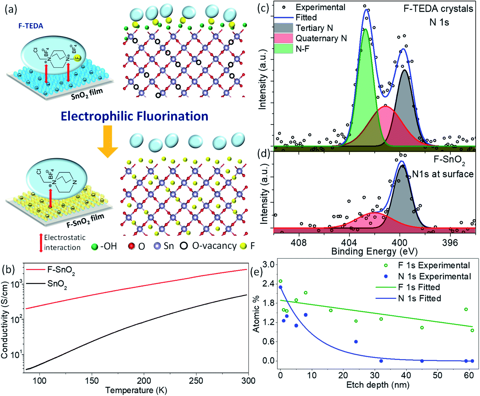 | ||
| Fig. 1 (a) Schematic demonstrating the fluorination process of the SnO2 film using the F-TEDA molecule as the fluorinating precursor. (b) Temperature-dependent conductivity of SnO2 and F–SnO2 films. (c and d) Deconvoluted N 1s HR-XPS spectra of the F-TEDA precursor compared with the F–SnO2 film. (e) Atomic % distribution versus etch depth for N 1s and F 1s across the F–SnO2 film. | ||
The high-resolution N 1s spectra of the F-TEDA molecule and the fluorinated SnO2 surface were examined as the N–F bond plays a major role in the fluorination process (Fig. 1c and d). The deconvoluted N 1s spectra of the F-TEDA precursor exhibit three peaks, quaternary-N (401.14 eV), tertiary-N (399.64 eV), and the third corresponding to the N–F bond (402.73 eV), as expected based on the structure of the molecule (Fig. 1c). Interestingly, the N 1s spectrum from the SnO2 originating due to the residual molecule bound to the film surface could be deconvoluted to two peaks only. The disappearance of the third peak at 402.73 eV indicates the structural changes after the release of fluorine species upon N–F bond dissociation (Fig. 1d). The N–F bond of F-TEDA is known to result in “F+” species that are highly reactive.50 This necessitates further probing of the SnO2 surface to explore various questions about whether the F-TEDA molecule adsorbs on the surface and releases fluorine to the SnO2 film or not. If in case fluorine diffuses inside the SnO2 film, further in-depth analysis of nitrogen and fluorine signals from the N–F bond is required for quantification. As shown in Fig. 1e, the nitrogen signal (for tertiary and quaternary nitrogen) falls exponentially and drops to the background value by an etch depth of ∼32 nm (ESI, Fig. S5†), indicating that the molecule is only absorbed on the surface and not incorporated into the SnO2 lattice. Moreover, the C 1s signal decreases in the same trend as N 1s (Fig. S6†), and it can be inferred that the signal originates from the surface-bound residual F-TEDA molecule after the release of fluorine species. The cationic part of the residual F-TEDA molecule is probably held to the negatively charged SnO2 surface with weak electrostatic interactions (schematic, Fig. 1a) as is observed for polyelectrolyte cations51 and polar dyes52 in the literature. However, a fluorine content of ∼2.49 at% on the surface falls off steadily to ∼1 at%, as analysed at a depth of 61 nm in the SnO2 lattice.
The XPS sputtering depth profile is obtained for understanding the chemical state and atomic concentration of fluorine present in F–SnO2 films. A broad peak of F 1s obtained at 684.5 eV is associated with Sn–F bonding (Fig. 2a). The solution-based fluorination process occurs throughout the depth of the SnO2 film. However, fluorination is generally assumed to be substitutional, involving the replacement of the oxygen vacancy by fluorine. Deconvolution of the F 1s peak is not only crucial for elucidating the nature of fluorination but also disentangling the contribution of substitutional and interstitial doping taking place in the SnO2 film. The F atom residing in the interstitial site occurs at higher binding energy than substitutional fluorine.32 In Fig. 2a, the F 1s peak for substitutional doping at 684.5 eV could be easily distinguished from the interstitial peak at 686.5 eV by the surface scan profile. The F 1s peak at different etch depths of 24 nm and 61 nm is shown in Fig. 2b and c, respectively, for highlighting the differences in fluorine distribution with respect to the depth of the film. It is interesting to relate the decrease in the amount of total fluorine to the interstitial fluorine since there is no significant change in the percentage of substitutional fluorine throughout the depth of the film examined (ESI, Fig. S7†). It can be clearly observed that substitutional doping (1.28 at%) remains nearly constant while interstitial doping (1.21 at%) decreases gradually with repeated sputtering cycles and falls off by 61 nm due to less diffusion of fluorine across the depth of the film, indicating that the process is surface-dominated (Fig. 2d). The diffusion length (L) of substitutional and interstitial fluorine in the F–SnO2 lattice is estimated by extrapolation of the depth profile data and the diffusion coefficient, D, is calculated using the relation 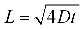 , where t is the reaction treatment time for fluorine diffusion to take place.53 Interestingly, substitutional fluorination exhibits one order higher diffusion coefficient of 7.1 × 10⁻¹⁴ cm2 s−1 than the interstitial one (2.5 × 10⁻¹⁵ cm2 s−1), which is understandable due to the energetically unfavourable interstitial doping in the compact rutile SnO2 structure.54,55
 | ||
| Fig. 2 Deconvoluted XPS spectra of F 1s from different etching depths of (a) 0 nm (at the surface), (b) 24 nm, and (c) 61 nm of F–SnO2, respectively. Spectra (a–c) are normalized to the maximum intensity. (d) Variation in substitutional and interstitial fluorine percentage present in the F–SnO2 lattice. | ||
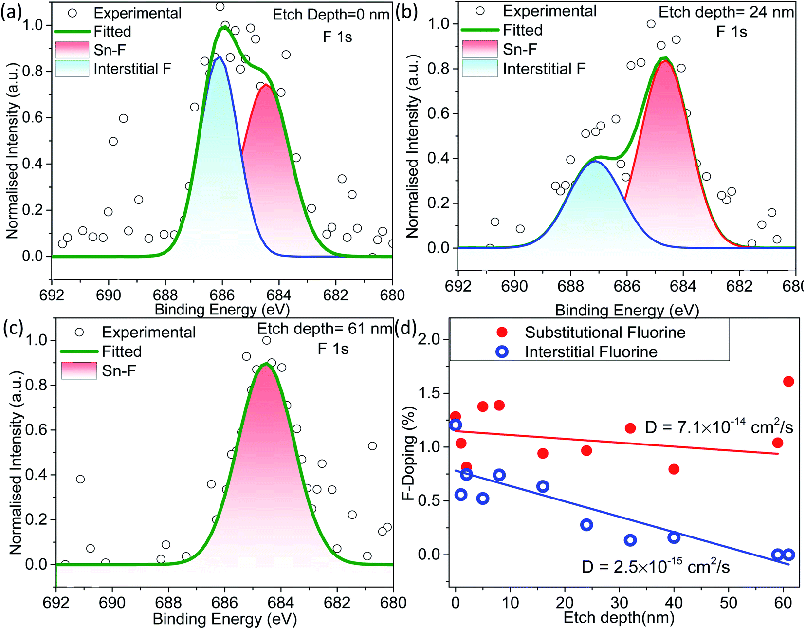
As seen from the line depth profile in Fig. 3a, Sn and O atoms are uniformly distributed with a constant Sn/O ratio of 0.51. The high-resolution Sn 3d5/2 spectra give information about the defects present in the pristine and fluorinated SnO2 (Fig. 3b and c). Sn 3d5/2 can be deconvoluted into two peaks at ∼486 eV (Sn2+) and ∼487 eV (Sn4+) in the SnO2 lattice.40 Sn2+ species in the SnO2 lattice are formed due to the insufficient oxygen component, thus acting as oxygen defects in the lattice.56 Pristine SnO2 is composed of a higher percentage of Sn2+ (∼25.6%) which is decreased to ∼3.9% in the F–SnO2 film. Moreover, there is an appearance of a third peak at 487.5 eV (Fig. 3c), which can be assigned to the Sn–F bond based on the literature.57 To further quantify the oxygen defects present in the pristine and F–SnO2 films, O 1s spectra of SnO2 and F–SnO2 are deconvoluted into three peaks, as shown in Fig. 3d and e. The first peak at ∼530 eV is related to the O in the SnO2 lattice (O–Sn4+) and the second peak at ∼533 eV is due to the adsorbed O species. The third peak at ∼531 eV is associated with the non-stoichiometric oxygen defects (O–Sn2+).24 The O 1s peak position and area under the curves for O–Sn2+ and O–Sn4+ are tabulated in Table S2.† It can be observed that the oxygen defects in pristine SnO2 (17.2%) passivate and are reduced to a mere 3.4% upon fluorination (Table S2†). The lower oxygen defect ratio in F–SnO2 is of significance for efficient electron transport in photoelectrochemical devices. Otherwise, these oxygen defects act as trap states and enhance the recombination of photogenerated charge carriers. PL and EPR studies were performed additionally to account for the oxygen defects in SnO2 before and after fluorination. In the PL spectra (Fig. S8†), F–SnO2 shows a significant decrease in the peaks at ∼410 nm and ∼463 nm, which is attributed to fluorine-mediated passivation of oxygen defects at mid band trap states (V++o and V0o). EPR shows a broad signal for SnO2 that disappears in F–SnO2 due to the reduction in oxygen defects (Fig. S9†).
 | ||
| Fig. 3 (a) Atomic percentages of Sn 3d and O 1s calculated from XPS of the F–SnO2 film at different depths. Deconvoluted XPS spectra of (b and c) Sn 3d5/2 and (d and e) O 1s of pristine SnO2 and F–SnO2, respectively. | ||
The DC and AC electrical properties of the SnO2 and F–SnO2 films are investigated to understand the role of fluorination. Fig. 4a shows symmetrical ohmic I–V characteristics with ∼2 order increase in current upon fluorination. The Nyquist plots show a single semi-circle corresponding to the granular thin films. The impedance data is fitted using an RC equivalent circuit with series contact resistance, RC (inset, Fig. 4b and c). The resistance RB represents the bulk resistance of the nanocrystalline film while capacitance from grain boundaries is replaced with a constant phase element, CPE, for fitting.58,59 The parameters are tabulated in ESI, Table S3.† The SnO2 film fits well to the equivalent circuit, while F–SnO2 exhibits a distorted semicircle in the high-frequency region, thus deviating slightly from the fitted curve. A drastic reduction in bulk resistance value of F–SnO2 (7.04 kΩ) in comparison to that of the SnO2 film (1598.8 kΩ) is observed upon fluorination similar to the changes observed in I–V measurements. The bulk resistance decreases with increasing temperature at each frequency more sharply for SnO2 as compared to F–SnO2 due to the thermally excited conduction mechanism and increase in scattering of charge carriers (Fig. S10†). In Fig. 4d, F–SnO2 shows higher capacitance than SnO2 over a wide frequency range without exhibiting any plateau region. The remarkable enhancement in the capacitance in F–SnO2 can be related to the increase in surface electron concentration from fluorine that effectively dominates the electrical charge transport.60 The high-frequency plateau in capacitance for SnO2 is attributed to the extrinsic contributions from grain boundaries.61 Furthermore, a two-order lower real impedance (Z′) reaffirms the high AC conductivity of F–SnO2 films (Fig. 4e). In F–SnO2, Z′ is purely resistive in nature over a wide frequency region as the barrier to capacitive grain boundaries and other defects is diminished by the increase in electronic charge concentration from fluorine, thus releasing the space charge that otherwise is present in SnO2 films.58 The imaginary impedance (−Z′′) versus frequency gives information of the electrical field relaxation time (τ) at the maximum frequency (fmax). The −Z′′ attains peak maximum at much higher frequency for F–SnO2 with ultrafast relaxation (0.27 μs) of charge carriers, resulting in high mobility and AC conductivity (Fig. 4e). With increasing temperature, the SnO2 film shows asymmetric broadening and shifting of the peaks with a decrease in −Z′′, indicating a temperature-dependent electrical relaxation process with the spread of relaxation times due to trap states, vacancies, and oxygen defects (Fig. S11†). Interestingly, the passivation of such defects in F–SnO2 minimizes the shift in  with increasing temperature (Fig. S12†). The activation energy (Ea) calculation from temperature-dependent imaginary impedance shows a dramatic reduction in the Ea value for the SnO2 film (240 meV) to 17.5 meV in F–SnO2 (Fig. 4f). These results are appreciable since the concentration of fluorine influences the electron density, thus increasing the conductivity and, consequently, activation energy decreases on fluorination.
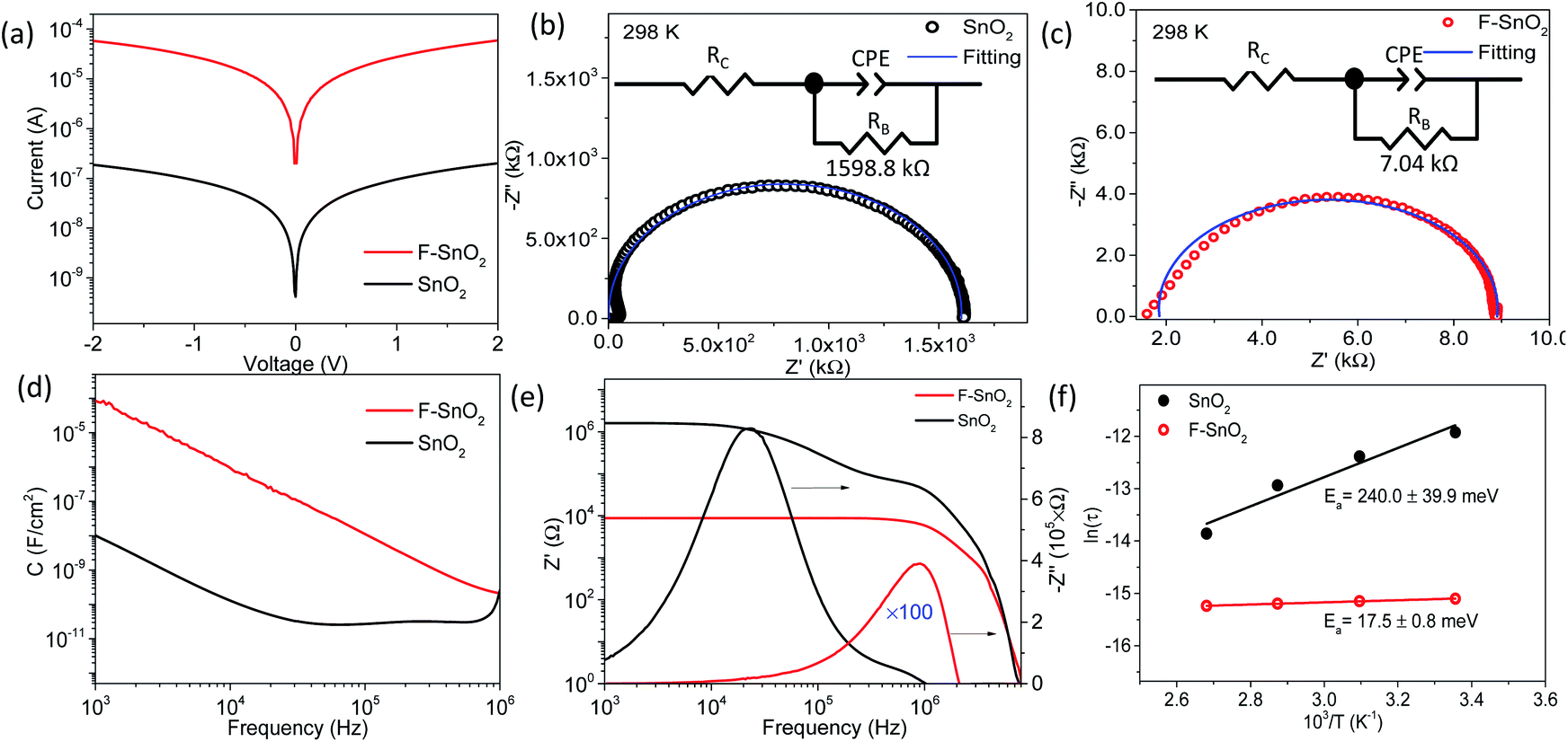 | ||
| Fig. 4 (a) I–V characteristics and (b and c) Nyquist plots of SnO2 and F–SnO2 films, respectively. Inset in (b and c) shows the equivalent circuit diagram used for fitting. (d) Capacitance versus frequency. (e) Real part (Z′) and imaginary part (−Z′′) of impedance as a function of frequency for SnO2 and F–SnO2 films. (f) Arrhenius plot of ln(τ) versus 1/T (K−1) obtained from impedance analysis at different temperatures. | ||
The SnO2 and F–SnO2 films show transmittance > 80% in the visible range (Fig. 5a, inset), making these suitable for optoelectronic device application. The bandgap of the F–SnO2 film is ∼3.71 eV, slightly higher than that of the SnO2 film (∼3.67 eV). The increase in the bandgap upon fluorination is due the filling of low-lying energy levels in the conduction band of F–SnO2, thus widening the bandgap. This is the Burstein–Moss effect well-known in the literature for transparent conducting oxides including fluorinated tin oxide.41 The electronic structure was studied by analysing the density of states below EF of pristine and F–SnO2 films (Fig. 5b). The band structures of SnO2 and F–SnO2 films differ significantly, as evident from the secondary electron cut-off (inset, left in Fig. 5b) and valence-edge spectra (inset, right in Fig. 5b). Upon fluorination, the VB shifts to lower energy, and EF is raised relative to the SnO2 film. The valence band edge (Eonset) is shifted to 3.9 eV in F–SnO2 with respect to the SnO2 (3.6 eV) film. The slope at the valence edge (lower cut-off BE) gives information about the oxygen defects (Sn2+ type species) in the SnO2 film, forming 5s and 5p hybrid states.62 The changes in the electronic density (reduction in slope) of the valence state upon fluorination can be attributed to substitutional doping of the SnO2 lattice by fluorine (observed in XPS), which reduces the oxygen defects, thus diminishing 5s–5p hybrid states. The shifting of the VB towards lower energies in F–SnO2 enhances its performance as an electron transport layer in PECs due to increased charge transport.63
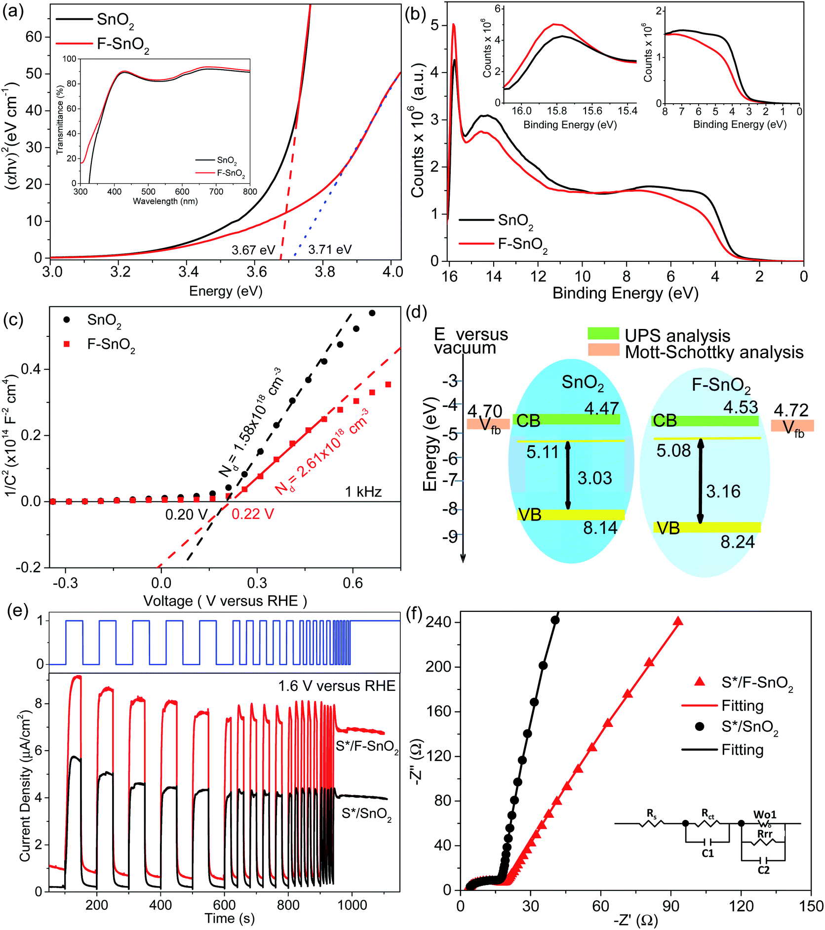 | ||
| Fig. 5 (a) Tauc plot for bandgap analysis and the corresponding UV-visible spectra (inset). (b) UPS survey spectra with the inset showing the magnified view of valence band spectra. (c) Mott–Schottky plots and (d) energy band diagram of pristine SnO2 and F–SnO2 films. (e) J–t measurements (at 1.6 V versus RHE) and (f) Nyquist plots of S*/SnO2 and S*/F–SnO2. Inset in f shows the equivalent circuit. | ||
Furthermore, to evaluate the flat band potential (Vfb) of the space charge region and the donor density (Nd), Mott–Schottky analysis of SnO2 and F–SnO2 was performed in neutral medium (0.5 M Na2SO4 solution) and calculated using the equation:64
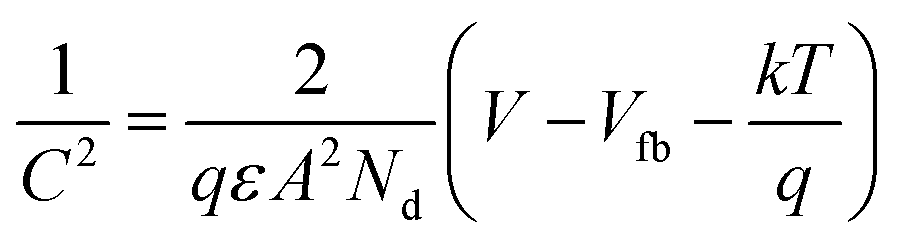 | (4) |
The electron transport property of the pristine SnO2 and F–SnO2 films on the FTO substrate was experimentally tested in a PEC by depositing CdS–TiO2 as a sensitizer (abbreviated as S*) following a pseudo-SILAR method. The UV-vis diffuse reflectance spectrum of CdS–TiO2 (S*) is shown in ESI, Fig. S13.† The photoelectrodes are annotated as S*/SnO2 and S*/F–SnO2 (shown in ESI, Fig. S14†). The photoresponse curves (J–t) of S*/SnO2 and S*/F–SnO2 at 1.6 V versus RHE with chopped light illumination are shown in Fig. 5e. Both the electrodes exhibit a spontaneous increase and decay in current density on exposure to varying input photo-pulses of the square waveform, suggesting a rapid transfer of the photogenerated electrons from the sensitizer (S*) to the current collector. It is interesting to observe a ∼81% increase in photocurrent density with the F–SnO2 (∼8.13 μA cm−2) electrode in comparison to that with SnO2 (∼4.47 μA cm−2). The photoresponse is even stable to continuous exposure of incident light for 150 seconds after the photo-pulse experiment. Similarly, the LSV curve at 5 mV s−1 for S*/F–SnO2 exhibits a higher photocurrent density than S*/SnO2 in the entire voltage range with a photocurrent density of 19.89 μA cm−2 and 7.41 μA cm−2, respectively at 1.6 V versus RHE (ESI, Fig. S15†). Such a significant increase in photocurrent density is due to the enhanced electron transport at the S*/F–SnO2 interface.
Electrochemical impedance spectroscopy (EIS) was performed to analyse the charge transfer processes occurring at the electrode–electrolyte interface. The Nyquist plots (Fig. 5f) under illumination conditions were fitted with the equivalent circuit (inset), and the derived values are tabulated in Table S4.†Rs is the series resistance at the interface of the photoanode material and the FTO substrate, while the parallel RCT and C1 elements give the charge transfer resistance. The capacitance in the semiconducting layer and the semiconductor–electrolyte interface is characterized by a double layer capacitance (C2) and a faradaic component (a charge transfer resistance, Rrr and Warburg element Wo), respectively. SnO2 exhibits large RCT and Rrr values of 13.4 Ω and 10.7 kΩ, respectively, which reduces to 12.8 Ω and 6.8 kΩ for F–SnO2. This enhanced charge transport in S*/F–SnO2 is a result of reduced recombination at the interface due to limited defects and enhancement in the donor density of F–SnO2.
In summary, the incorporation of fluorine into the SnO2 lattice could be observed in two ways i.e. substitutional and interstitial. The substitutional fluorine occupies the place of oxygen in the SnO2 lattice (due to the comparable size of O2− and F−), thus passivating the oxygen vacancies which are present as defects in the lattice.48 On the other hand, the insertion of fluorine in the interstitial site of the SnO2 lattice does not influence the oxygen defects; rather, it is known to have pernicious effects by limiting the achievable mobility of the charge carriers.32 F–SnO2 as the charge transport layer shows ∼81% increase in the photocurrent density and decrease in charge transfer resistance by ∼36%. This enhancement in the photocurrent density is because of the reduction in the recombination losses of charge carriers in F–SnO2 films, which is expected due to the decrease in the oxygen vacancies which act as trap states for the charge carrier and increase in the electrical conductivity upon substitutional fluorination. The shifting of the valence band towards lower energies in F–SnO2 further limits charge recombination and enhances the charge transport at the sensitizer–SnO2 interface.
4 Conclusion
In conclusion, we have successfully doped fluorine into SnO2 films using F-TEDA as a fluorinating precursor by the solution processing method. The fluorinated SnO2 films are studied using highly powerful surface-sensitive techniques (XPS and UPS) for understanding the effect of fluorine on the composition and electronic band structure of SnO2. The nature of fluorine doping (∼2.49 at%) is examined across the depth of the SnO2 film. Apart from substitutional fluorine, the surface of the F–SnO2 film is enriched with interstitial fluorine (1.21 at%) that decays completely by 61 nm depth. The incorporation of fluorine passivates the surface defects in the SnO2 film, increases the electrical conductivity by two orders of magnitude and drastically reduces the activation energy to 17.5 meV. The F–SnO2 layer enhances the electron transport from the photoactive CdS–TiO2 sensitizer to the electrode, resulting in a significantly suppressed electron accumulation and excellent PEC performance. Fluorination is a promising strategy towards defect passivation in charge transport layers and is of significant importance in optoelectronic devices.Conflicts of interest
There are no conflicts to declare.Acknowledgements
The authors are grateful to Professor G. U. Kulkarni (JNCASR, Bangalore) and Dr Rakesh K. Sharma (IIT Jodhpur) for their constant motivational support and encouragement. Indrajit Mondal (CeNS, Bangalore) is acknowledged for SEM measurements. Authors acknowledge the Department of Chemistry and Centre for Advanced Scientific Equipment, IIT Jodhpur, for laboratory and characterization facilities. The financial support from SERB, CRG/2020/003465 is gratefully acknowledged. MV thanks IIT Jodhpur for the student fellowship, and GB thanks the SERB grant, CRG/2020/003465, for the Postdoctoral Fellowship.References
- L. Finegold and J. L. Cude, Nature, 1972, 238, 38–40 CrossRef CAS PubMed.
- C. Jiang, S. J. A. Moniz, A. Wang, T. Zhang and J. Tang, Chem. Soc. Rev., 2017, 46, 4645–4660 RSC.
- M. Law, L. E. Greene, J. C. Johnson, R. Saykally and P. Yang, Nat. Mater., 2005, 4, 455–459 CrossRef CAS PubMed.
- J. Du, J. Qi, D. Wang and Z. Tang, Energy Environ. Sci., 2012, 5, 6914–6918 RSC.
- Y. Bai, I. Mora-Seró, F. De Angelis, J. Bisquert and P. Wang, Chem. Rev., 2014, 114, 10095–10130 CrossRef CAS PubMed.
- Z. Bai, X. Yan, Y. Li, Z. Kang, S. Cao and Y. Zhang, Adv. Energy Mater., 2016, 6, 1–8 Search PubMed.
- W. Wang, C. Jin and L. Qi, Small, 2018, 14, 1–10 Search PubMed.
- S. Sahu and S. Chandra, Sol. Cells, 1987, 22, 163–173 CrossRef CAS.
- W. Li, P. Da, Y. Zhang, Y. Wang, X. Lin, X. Gong and G. Zheng, ACS Nano, 2014, 8, 11770–11777 CrossRef CAS PubMed.
- H. Dotan, K. Sivula, M. Grätzel, A. Rothschild and S. C. Warren, Energy Environ. Sci., 2011, 4, 958–964 RSC.
- T. Kim and K. Choi, Science, 2014, 343, 990–994 CrossRef CAS PubMed.
- K. T. Fountaine, H. J. Lewerenz and H. A. Atwater, Nat. Commun., 2016, 7, 1–9 Search PubMed.
- M. Radecka, A. Wnuk, A. Trenczek-Zajac, K. Schneider and K. Zakrzewska, Int. J. Hydrogen Energy, 2015, 40, 841–851 CrossRef CAS.
- H. Wang, H. Li, S. Cao, M. Wang, J. Chen and Z. Zang, Sol. RRL, 2020, 4, 2000226 CrossRef CAS.
- X. Hu, H. Wang, M. Wang and Z. Zang, Sol. Energy, 2020, 206, 816–825 CrossRef CAS.
- S. Cao, H. Wang, H. Li, J. Chen and Z. Zang, Chem. Eng. J., 2020, 394, 124903 CrossRef CAS.
- H. Wang, H. Li, W. Cai, P. Zhang, S. Cao, Z. Chen and Z. Zang, Nanoscale, 2020, 12, 14369–14404 RSC.
- H. C. Shin, J. Dong and M. Liu, Adv. Mater., 2004, 16, 237–240 CrossRef CAS.
- J. Y. Kim, J. S. Kang, J. Shin, J. Kim, S. J. Han, J. Park, Y. S. Min, M. J. Ko and Y. E. Sung, Nanoscale, 2015, 7, 8368–8377 RSC.
- Z. Zhang, C. Gao, Z. Wu, W. Han, Y. Wang, W. Fu, X. Li and E. Xie, Nano Energy, 2016, 19, 318–327 CrossRef CAS.
- L. Xiong, Y. Guo, J. Wen, H. Liu, G. Yang, P. Qin and G. Fang, Adv. Funct. Mater., 2018, 28, 1–18 Search PubMed.
- M. F. Mohamad Noh, N. A. Arzaee, J. Safaei, N. A. Mohamed, H. P. Kim, A. R. Mohd Yusoff, J. Jang and M. A. Mat Teridi, J. Alloys Compd., 2019, 773, 997–1008 CrossRef CAS.
- J. Wang, K. Datta, C. H. L. Weijtens, M. M. Wienk and R. A. J. Janssen, Adv. Funct. Mater., 2019, 29, 1905883 CrossRef CAS.
- E. Jiang, Y. Ai, J. Yan, N. Li, L. Lin, Z. Wang, C. Shou, B. Yan, Y. Zeng, J. Sheng and J. Ye, ACS Appl. Mater. Interfaces, 2019, 11, 36727–36734 CrossRef CAS PubMed.
- Y. Luan, X. Yi, P. Mao, Y. Wei, J. Zhuang, N. Chen, T. Lin, C. Li and J. Wang, iScience, 2019, 16, 433–441 CrossRef CAS PubMed.
- J. Liang, Z. Chen, G. Yang, H. Wang, F. Ye, C. Tao and G. Fang, ACS Appl. Mater. Interfaces, 2019, 11, 23152–23159 CrossRef CAS.
- E. Mokaripoor and M. M. Bagheri-Mohagheghi, Mater. Sci. Semicond. Process., 2015, 30, 400–405 CrossRef CAS.
- B. Zhang, Y. Tian, J. X. Zhang and W. Cai, Vacuum, 2011, 85, 986–989 CrossRef CAS.
- T. T. Nguyen, H. P. Dang, Q. H. Luc and T. Le, Ceram. Int., 2019, 45, 9147–9156 CrossRef CAS.
- H. Tan, A. Jain, X. Lan, F. P. G. Arquer, J. Z. Fan, R. Quintero-Bermudez, M. Yuan, B. Zhang, Y. Zhao, F. Fan, P. Li, L. N. Quan, Y. Zhao, Z. Lu, Z. Yang, S. Hoogland and E. H. Sargent, Science, 2017, 355, 722–726 CrossRef CAS PubMed.
- P. Karthick, K. Saravanakumar, C. Sanjeeviraja and K. Jeyadheepan, Thin Solid Films, 2020, 713, 138362 CrossRef CAS.
- J. E. N. Swallow, B. A. D. Williamson, T. J. Whittles, M. Birkett, T. J. Featherstone, N. Peng, A. Abbott, M. Farnworth, K. J. Cheetham, P. Warren, D. O. Scanlon, V. R. Dhanak and T. D. Veal, Adv. Funct. Mater., 2018, 28, 1–10 CrossRef.
- A. K. Saxena, R. Thangaraj, S. P. Singh and O. P. Agnihotri, Bull. Mater. Sci., 1986, 8, 315–318 CrossRef CAS.
- X. Wang, X. Wang, Q. Di, H. Zhao, B. Liang and J. Yang, Materials, 2017, 10, 1398 CrossRef.
- H. Wang, K. Dou, W. Y. Teoh, Y. Zhan, T. F. Hung, F. Zhang, J. Xu, R. Zhang and A. L. Rogach, Adv. Funct. Mater., 2013, 23, 4847–4853 CAS.
- N. Noor, C. K. T. Chew, D. S. Bhachu, M. R. Waugh, C. J. Carmalt and I. P. Parkin, J. Mater. Chem. C, 2015, 3, 9359–9368 RSC.
- N. Noor and I. P. Parkin, J. Mater. Chem. C, 2013, 1, 984–996 RSC.
- J. H. Kim, S. Yonezawa and T. Okada, Chem. Lett., 2018, 47, 393–395 CrossRef CAS.
- C. Wyse, R. Torres, T. Barnes, M. Scott, M. Young, X. Li and T. Gessert, 2009 34th IEEE Photovoltaic Specialists Conference (PVSC), IEEE, 2009, pp. 002435–002438 Search PubMed.
- T. Jäger, Y. E. Romanyuk, A. N. Tiwari and A. Anders, J. Appl. Phys., 2014, 116, 033301 CrossRef.
- Z. Banyamin, P. Kelly, G. West and J. Boardman, Coatings, 2014, 4, 732–746 CrossRef.
- G. C. Morris and A. E. McElnea, Appl. Surf. Sci., 1996, 92, 167–170 CrossRef CAS.
- G. Bahuguna, I. Mondal, M. Verma, M. Kumar, S. Bhattacharya, R. Gupta and G. U. Kulkarni, ACS Appl. Mater. Interfaces, 2020, 12, 37320–37329 CrossRef CAS PubMed.
- G. Bahuguna, S. Chaudhary, R. K. Sharma and R. Gupta, Energy Technol., 2019, 7, 1–8 CrossRef.
- M. P. Genovese, I. V. Lightcap and P. V. Kamat, ACS Nano, 2012, 6, 865–872 CrossRef CAS PubMed.
- M. Park, J. Y. Kim, H. J. Son, C. H. Lee, S. S. Jang and M. J. Ko, Nano Energy, 2016, 26, 208–215 CrossRef CAS.
- V. H. Tran, R. B. Ambade, S. B. Ambade, S. H. Lee and I. H. Lee, ACS Appl. Mater. Interfaces, 2017, 9, 1645–1653 CrossRef CAS PubMed.
- T. Rhimi, M. Toumi, K. Khirouni and S. Guermazi, J. Alloys Compd., 2017, 714, 546–552 CrossRef CAS.
- P. V. Bhuvaneswari, P. Velusamy, R. R. Babu, S. M. Babu, K. Ramamurthi and M. Arivanandhan, Mater. Sci. Semicond. Process., 2013, 16, 1964–1970 CrossRef CAS.
- S. D. Taylor, C. Christopher and G. Hum, Tetrahedron, 1999, 55, 12431–12477 CrossRef CAS.
- S. Zhan, D. Li, S. Liang, X. Chen and X. Li, Sensors, 2013, 13, 4378–4389 CrossRef CAS PubMed.
- A. Huda, I. P. Mahendra, R. Ichwani, C. T. Handoko, H. M. Ngoc, B. Yudono, M. D. Bustan and F. Gulo, Rasayan J. Chem., 2019, 12, 308–318 CrossRef CAS.
- J. B. Gilbert, M. F. Rubner and R. E. Cohen, Proc. Natl. Acad. Sci. U. S. A., 2013, 110, 6651–6656 CrossRef CAS PubMed.
- Y. Kang and C. G. Van de Walle, Appl. Phys. Lett., 2017, 111, 152107 CrossRef.
- D. R. Acosta, E. P. Zironi, E. Montoya and W. Estrada, Thin Solid Films, 1996, 288, 1–7 CrossRef CAS.
- M. Kwoka, L. Ottaviano, M. Passacantando, S. Santucci, G. Czempik and J. Szuber, Thin Solid Films, 2005, 490, 36–42 CrossRef CAS.
- J. Kim, A. Ho-Baillie and S. Huang, Sol. RRL, 2019, 3, 1–16 Search PubMed.
- W. Shen, T. Ou, J. Wang, T. Qin, G. Zhang, X. Zhang, Y. Han, Y. Ma and C. Gao, Sci. Rep., 2018, 8, 5086 CrossRef PubMed.
- D. K. Bandgar, S. T. Navale, M. Naushad, R. S. Mane, F. J. Stadler and V. B. Patil, RSC Adv., 2015, 5, 68964–68971 RSC.
- M. A. Ponce, P. R. Bueno, J. Varel, M. S. Castro and C. M. Aldao, J. Mater. Sci.: Mater. Electron., 2008, 19, 1169–1175 CrossRef CAS.
- M. Coskun, O. Polat, F. M. Coskun, Z. Durmus, M. Çaglar and A. Turut, RSC Adv., 2018, 8, 4634 RSC.
- H. Che and M. El Bouanani, Nucl. Instrum. Methods Phys. Res., Sect. B, 2018, 414, 170–175 CrossRef CAS.
- M. F. Aygüler, A. G. Hufnagel, P. Rieder, M. Wussler, W. Jaegermann, T. Bein, V. Dyakonov, M. L. Petrus, A. Baumann and P. Docampo, ACS Appl. Mater. Interfaces, 2018, 10, 11414–11419 CrossRef PubMed.
- F. Mohamadkhani, S. Javadpour and N. Taghavinia, Sol. Energy, 2019, 191, 647–653 CrossRef CAS.
Footnotes |
| † Electronic supplementary information (ESI) available. See DOI: 10.1039/d1ta02560k |
| ‡ Both authors contributed equally. |
| This journal is © The Royal Society of Chemistry 2021 |