
Synergistic incorporation of NaF and CsF PDT for high efficiency kesterite solar cells: unveiling of grain interior and grain boundary effects†
Xiaohuan
Chang‡
a,
Junjie
Fu‡
a,
Dongxing
Kou
 *a,
Wenhui
Zhou
a,
Zhengji
Zhou
a,
Shengjie
Yuan
a,
Yafang
Qi
a,
Zhi
Zheng
b and
Sixin
Wu
*a
*a,
Wenhui
Zhou
a,
Zhengji
Zhou
a,
Shengjie
Yuan
a,
Yafang
Qi
a,
Zhi
Zheng
b and
Sixin
Wu
*a
aKey Lab for Special Functional Materials, Ministry of Education, National & Local Joint Engineering Research Center for High-Efficiency Display and Lighting Technology, School of Materials Science and Engineering, Collaborative Innovation Center of Nano Functional Materials and Applications, Henan University, Kaifeng 475004, China. E-mail: koudongxing@henu.edu.cn; wusixin@henu.edu.cn
bInstitute of Surface Micro and Nano Materials, College of Advanced Materials and energy, Key Laboratory of Micro-Nano Materials for Energy Storage and Conversion of Henan Province, Xuchang University, Xuchang, Henan, 461000, China
First published on 21st November 2020
Abstract
The introduction of alkali metal (AM) post-deposition treatment (PDT) has led to the consecutive breakthrough of world record efficiencies for Cu(In,Ga)Se2 photovoltaics. However, for the derivative Cu2SnZn(S,Se)4 (CZTSSe) solar cells, the corresponding verdict seems partially unjustified due to the difference in defect chemical environment and phase structure, and the most effective incorporation means of AMs is still a mystery. In this work, for the first time, we developed a dual AM synergistic incorporation strategy combining light and heavy AMs by post-depositing CsF after NaF-PDT to improve the efficiency of CZTSSe solar cells. The relevant microscopic-electrical advantages with regard to the different roles of NaF and CsF PDT are discussed in more detail. It was found that the Na atoms are randomly dispersed both in the grain interior (GI) and grain boundaries (GBs), significantly increasing the acceptor concentration and passivating the deep level defects to enhance the Voc. In contrast, the Cs atoms are mainly segregated at the GBs, primarily increasing the potential of the GBs and improving the FF. The prominent electric benefits of Cs at the GBs and Na in the GI finally increase the device efficiency from 10.12% to 12.16%. Our findings solve the difficulty in obtaining the available Voc and FF for future high efficiency research and should serve as a basis for the in-depth understanding of AM-PDT in kesterite photovoltaics.
1. Introduction
The earth abundant, nontoxic kesterite Cu2SnZn(S,Se)4 (CZTSSe) solar cells are a promising option in next-generation PV technologies.1–5 However, their state-of-the-art efficiency of 12.62% achieved in 2019 is still far behind the 23.35% efficiency for Cu(In,Ga)Se2 (CIGS) solar cells sharing a similar structure.6,7 Due to the inherent high popular bulk defects/defect clusters and unfavorable interface/grain boundary (GB) problems,8–12 both the relatively low open-circuit voltage (Voc) and fill factor (FF) remain the key issues hindering the kesterite PV from approaching the Shockley–Queisser (SQ) limit.13,14Alkali metal (AM) dopants in chalcopyrite solar cells can effectively facilitate hot-carrier cooling and minimize the native defect-mediated radiative recombination,15 which has experimentally shown remarkable enhancement in PV performance.16 Considering the mature development history of CIGS solar cells, the earliest doped AM is sodium by increasing the net doping levels to improve the Voc and FF.17 Subsequently, consecutive breakthrough of world record efficiencies of 22.3%,18 22.6%,19 and 23.35%7 beyond this effect were achieved through KF, RbF, and CsF post-deposition treatments (PDT),7,18,19 respectively. It has been completely accepted that the heavy alkalis (K, Rb, and Cs) are more influential than light alkalis (Li and Na) to improve the device performance for CIGS PV.17,19,20 Besides the modification of the associated bulk carrier concentration enhancement,21,22 defect passivation and grain boundary (GB) potential similar to that of light AMs,23,24 the greatest advantage of heavy AM-PDT on CIGS absorber is the enhanced Cu depletion at the micro-nano surface.25–27 The formed AM–In–Se compound broadens the surface band gap,28–30 decreases the valence band maximum (VBM), and further suppresses carrier recombination at the p–n junction.31,32
However, for their derivative CZTS solar cells, these verdicts seem partially unjustified. Despite the similar order of Rb > Na > Li reported,33 the most attractive alkali is still Na, and increasing research demonstrates that light alkalis are more applicable for the kesterite system.34–38 In some solution systems (DMSO processed), the alternative light alkali metal Li is also more effective than heavy alkalis to increase the device efficiency up to 12%, and its specialty is expected to tune the bandgap by alloying into the kesterite phase and inverse the band bending around GBs by forming wide band gap Li-relevant compounds.39–41 These results imply that the electric enhancement by AM-PDT on CIGS is not inherited entirely for the CZTS system. The surface Cu depletion layer cannot be formed due to the concentrated CuZn defects with the lowest formation energy at the surface absorber.42 Several studies attempted to disclose the different effects of various AMs on the properties of kesterite PV, but different rankings with no consistent results have been obtained.41,43,44 Experimental observations indicate that the exact role of alkali elements for performance enhancement mainly relies on the chemical environment, absorber constituent and annealing temperature.21,45,46 Nevertheless, these macroscopic findings are difficult to be implemented in practical applications, and the most potential alkali element for efficiency improvement is still a mystery. Therefore, in-depth understanding of the evolution of the structural and electrical properties of the kesterite absorber after AM-PDT down to the atomic scale is essential for future breakthrough in the state-of-the-art efficiency.
In this work, different AMs (Li, Na, K, Rb and Cs) were incorporated into CZTSSe solar cells to improve their PV performance, and the synchronous evolution of alkali element distribution, defect chemical environment and grain boundary (GB) potential are synthetically described. A ranking of Na > K > Cs > Rb > Li was obtained for the best device performances. By carefully comparing their PV parameters, it was found that the light AMs (Li and Na) and heavy AMs (K, Rb and Cs) possess different functional mechanisms, wherein light AMs (especially Na) result in a remarkable enhancement in Voc, while the heavy AMs are more inclined to improve the fill factor (FF). In-depth observations revealed that the Na ion with a smaller migration energy is randomly dispersed in both the grain interior (GI) and GBs, significantly increasing the acceptor concentration and passivating the deep level defects. On the other hand, the heavy AMs are predominantly segregated at the GBs via ion exchange and have a more profound influence on the GB potential. Based on their electric disparity in defect-mediated charge recombination and GB-dominant carrier transport processes, we propose for the first time the synergistic incorporation of NaF-PDT and CsF-PDT into the CZTSSe system and the device efficiency finally increased up to 12.16%.
2. Experimental section
2.1 Materials
Copper powder (Cu, 99.9%) was purchased from Macklin Company. Zinc powder (Zn, 99.9%), tin powder (Sn, 99.9%), sulfur powder (S, 99.95%), selenium powder (Se, 99.9%), cadmium sulfate, 8/3-hydrate (CdSO4·8/3H2O, 99%), thiourea (NH2CSNH2, 99%), 2-methoxyethanol (C3H8O2, 99.7%), ethanolamine (C2H7NO, 99.5%), mercaptoacetic acid (C2H4O2S, 98%), lithium fluoride (LiF, 99.9%) sodium fluoride (NaF, 99%), potassium fluoride (KF, 99.5%), rubidium fluoride (RbF, 99.8%) and cesium fluoride (CsF, 99.9%) were purchased form Aladdin Company. Ammonia solution (NH4OH, 25%) was obtained from Kaifeng Dongda Company. 2-Ethanedithiol (HSCH2CH2SH, 98%) and 1,2-ethylenediamine (H2NCH2CH2NH2, 99%) were obtained from Alfa Aesar Chemical Company. All chemical reagents were used directly.2.2 Preparation of CZTSSe precursor solution
Firstly, 0.699 g Cu, 0.494 g Zn, 0.0858 g Sn, 0.0857 g S and 0.0234 g Se were added directly to a 25 mL round-bottom flask. Next, 0.5 mL 1,2-ethanedithiol and 5.0 mL 1,2-ethylenediamine were injected. The mixture was stirred at 700 rpm for 1.5 h at 70 °C until a transparent wine red solution was formed. Then 1 mL stabilizer solution (the volumetric ratio of ethanolamine![[thin space (1/6-em)]](https://www.rsc.org/images/entities/char_2009.gif) :thioglycolic acid:glycol methyl ether is 1:1:2) was injected into the round-bottom flask, and the solution was kept stirring for 0.5 h until a transparent CZTSSe precursor solution was obtained.
:thioglycolic acid:glycol methyl ether is 1:1:2) was injected into the round-bottom flask, and the solution was kept stirring for 0.5 h until a transparent CZTSSe precursor solution was obtained.
2.3 Preparation of CZTSSe thin film
The CZTSSe thin film was prepared by spin-coating the precursor solution on a molybdenum-coated soda lime glass substrate (20 mm × 20 mm × 1.1 mm) at 3000 rpm for 30 s and then sintering on a hotplate at 310 °C for 2 min in a glove box. The spin coating and sintering processes were repeated nine times to obtain a CZTSSe precursor film with ∼2 μm thickness. The obtained precursor thin films were put into a closed square graphite box containing sufficient selenium particles and selenized at 550 °C for 15 min in a rapid thermal processing (RTP) tube furnace under a nitrogen atmosphere. AM-PDT was generally performed by evaporating 5 nm LiF, NaF, KF, RbF or CsF layer on the as-prepared CZTSSe film. Finally, a heat treatment was needed to facilitate the diffusion of AM atoms into the bulk absorber, and thus the films were put in a closed square graphite box containing sufficient selenium particles and heated at 350 °C for 5 min in RTP tube furnace under nitrogen atmosphere. During the selenization and PDT processes, excess Se particles were used to ensure the selenium vapor pressure and prevent degradation of the kesterite CZTSSe. As seen in Fig. S1,† 480 mg and 320 mg selenium particles were placed in the holes of the graphite box for the selenization and PDT treatment, respectively. Both were filled with N2 at the flow rate of 80 sccm. To obtain a fresh surface, the AM-PDT samples were soaked in deionized water for 5 min to remove the residual alkali metal and dried under an N2 flow. These samples were directly sealed in an N2-filled hermetic bag to minimize the surface contamination before performing other measurements.2.4 Device fabrication
The CZTSSe device was fabricated in the structure of soda lime glass/Mo/CZTSSe absorber/CdS/ZnO/ITO/Ag/MgF2. In detail, 50 nm CdS was deposited on top of the CZTSSe absorber via a chemical bath deposition method. Subsequently, a 50 nm ZnO and 180 nm ITO layer were successively sputtered using magnetron sputtering. Finally, a 200 nm Ag grid electrode for current collection and 70 nm MgF2 antireflection coating were thermally evaporated on top. The sample was mechanically divided into nine devices and the effective area of each device was 0.21 cm2 (Fig. S2†).2.5 Characterization
The phase structure of the CZTSSe film was characterized via X-ray diffraction (D8-ADVANCE). The surface and cross-section morphology of the thin films were detected using a field emission scanning electron microscope (SEM, Nova Nano SEM 450). Current–voltage measurements were performed on a solar simulator with a 150 W xenon lamp. Electrochemical impedance spectroscopy (EIS) was performed at −0.4 V bias using a frequency response analyzer (FRA) equipped with a PGSTAT 302N (AUTO LAB). Capacitance–voltage curves and deep-level transient spectra were obtained using a HERA-DLTS system from Phys. Tech. Kelvin probe force microscopy (KPFM) analysis was performed on an atomic force microscope from Bruker to obtain the surface potential and morphology. During the measurement, the samples were kept in a nitrogen atmosphere filled glove box with the oxygen concentration and humidity below 1.0 ppm. The non-contact mode under an AC voltage with amplitude of 1.0 V was applied at room temperature. The external quantum efficiency (EQE) response was measured using a Zolix SCS100 QE system. The scanning wavelength range was 300–1400 nm. Static secondary ion mass spectrometry (TOF-SIMS) was used to characterize the composition distribution profile within the device. X-ray photoelectron spectroscopy (XPS) depth profiles of the reference and CsF-PDT CZTSSe films were measured on a Thermo Fischer, ESCALAB Xi+ system at 12.5 kV and 16 mA with a monochromatic Al Kα X-ray (1486.6 eV) beam a vacuum of 8 × 10⁻¹⁰ Pa. Scanning transmission electron microscopy (STEM) measurement was performed with a FEI Titan3 Cubed G2 60–300 aberration-corrected STEM instrument.3. Results and discussion
Due to the component dependence of alkali metals, the composition of the selenized absorber was identified by inductively coupled plasma (ICP) emission spectrometry (Table S1†), and the samples generally demonstrated a Cu-poor/Zn-rich structure with Cu/(Sn + Zn) ratio of 0.77 and Zn/Sn ratio of 1.08. To execute the proposed light-heavy AM synergistic dopant strategy, the optimal incorporation condition and the independent effect of different AM-PDT (Li, Na, K, Rb and Cs) on the device performance needed to be initially verified. By comparing the statistical distributions of the device efficiencies at different PDT temperatures, times and thicknesses for all types of alkali metals, as presented in Fig. S3–S7,† it can be inferred that the universal incorporation condition for AM-PDT is 350 °C, 5 min and 5 nm, respectively. During the PDT procedure, selenium atmosphere protection was needed to prevent the degradation of the CZTSSe absorber (Fig. 1a). The XRD, Raman and SEM measurements shown in Fig. S8 and S9† demonstrate that the phase structure and morphology of the selenized CZTSSe films were unchanged after the different AM-PDT.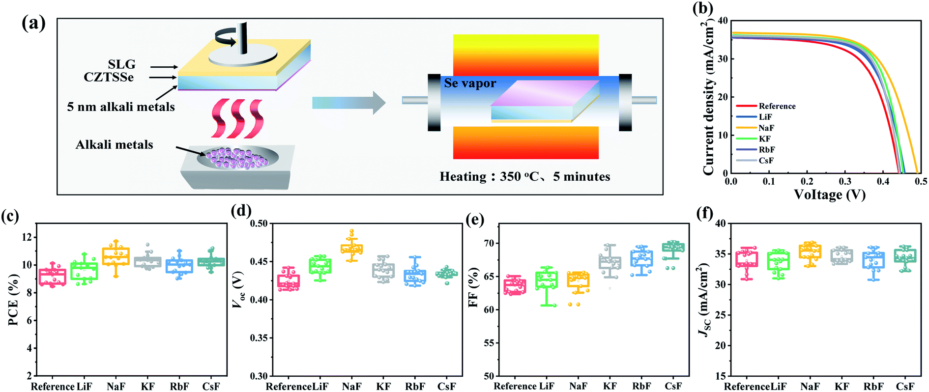 | ||
| Fig. 1 (a) Schematic diagram of the alkali metal post-deposition treatment procedure. (b) J–V curves of CZTSSe thin film solar cells with different AM-PDT. Statistical box diagrams of (c) PCE, (d) Voc, (e) FF, and (f) Jsc derived from 15 devices for each type of solar cell. | ||
Fig. 1b–f and Table 1 present the J–V curves and the relevant statistical distribution of the photovoltaic parameters for the CZTSSe solar cells with different AM-PDT. A ranking of Na > K > Cs > Rb > Li > reference was obtained for the best device performances. To distinguish additional effects from the effect of the PDT thermal treatment, the I–V properties of the CZTSSe solar cells before and after PDT thermal treatment without AM layer deposition were further compared, as shown in Fig. S10.† The result demonstrates the fact that an independent thermal treatment at this condition (350 °C, 5 min) would slightly degrade device efficiency due to the volatilization of the Sn element, further supporting the beneficial effects of AM incorporation on the PV performance improvement. The alkali elements Na and Cs seem to be the most favorable light AMs and heavy AMs for CZTSSe system by increasing Voc and FF, respectively. By carefully comparing the resulting PV parameters, it is meaningful to find that sodium significantly increased the shunt resistance Rsh from 742 Ω cm2 to 1612 Ω cm2, while cesium reduced the series resistance Rs more notably from 0.87 Ω cm2 to 0.26 Ω cm2, implying their functional mechanism on charge recombination and transport behavior is distinct from each other. In the case of the least effective light AM Li, several studies proposed that it just alters the electrical properties of kesterite films at a high dopant level,47 and the nearly unchanged carrier concentration in Fig. S11† further supports this conjecture.
| Cell | PCE (%) | FF (%) | V oc (mV) | J sc (mA) | R sh (Ω cm2) | R s (Ω cm2) | A |
|---|---|---|---|---|---|---|---|
| Reference | 10.12 | 64.41 | 442 | 35.56 | 742 | 0.87 | 1.98 |
| Li | 10.78 | 66.30 | 457 | 35.58 | 1215 | 0.65 | 1.63 |
| Na | 11.71 | 64.86 | 490 | 36.86 | 1612 | 0.85 | 1.82 |
| K | 11.46 | 69.87 | 453 | 36.22 | 1095 | 0.27 | 1.51 |
| Rb | 11.02 | 69.50 | 445 | 35.64 | 785 | 0.29 | 1.52 |
| Cs | 11.20 | 70.19 | 443 | 36.02 | 775 | 0.26 | 1.45 |
As illustrated in Fig. 2a, the selenized CZTSSe absorber generally exhibits a bilayer structure with a large grain layer on top and fine grain layer at the bottom. During the PDT process, a large amount of surface AM ions migrate into the bulk absorber via a copper vacancy (VCu)-mediated mechanism.15,47 The depth distribution profiles of the Na and Cs elements for the NaF-PDT and CsF-PDT CZTSSe solar cells were characterized by time-of-flight secondary ion mass spectrometry (TOF-SIMS), respectively. As shown in Fig. 2b–d, the diffused Na and Cs elements were dispersed throughout the absorber after high temperature annealing, and the initial Na level originating from the soda-lime glass (SLG) in the CsF-PDT device became slightly lower than that of the reference sample. Meanwhile, the observed depth profiles of Cu, Zn, Sn, S and Se were all nearly unchanged within the NaF-PDT and CsF-PDT devices, and most of the alkali metals ions diffused into the fine grain layer. The unchanged absorber morphology after PDT and strong tolerance of alkali metals within the fine grain layer led to the lower dependence of the device performance on the variation of alkali metals at a certain content. These properties helped us to use the same PDT condition for different alkali metals species and ensured their optimal device performance, which is different from some other systems41 with strong and distinct dependence on concentration for different alkali metals. Additionally, the XPS elemental depth profiles of the reference and CsF-PDT CZTSSe films are provided in Fig. S12† to further identify the evolution of the surface elemental composition after alkali metal post-deposition treatment. It can be found that the surface Cu content was lower than that of bulk absorber for both samples, and this situation became more evident after CsF-PDT. However, the reduced scope of the off-stoichiometric micro-nano surface would be restricted within the thermodynamic limit of the kesterite phase due to its narrower stable phase region48 and a fairly Cu-depletion surface49 is still hard to be formed.
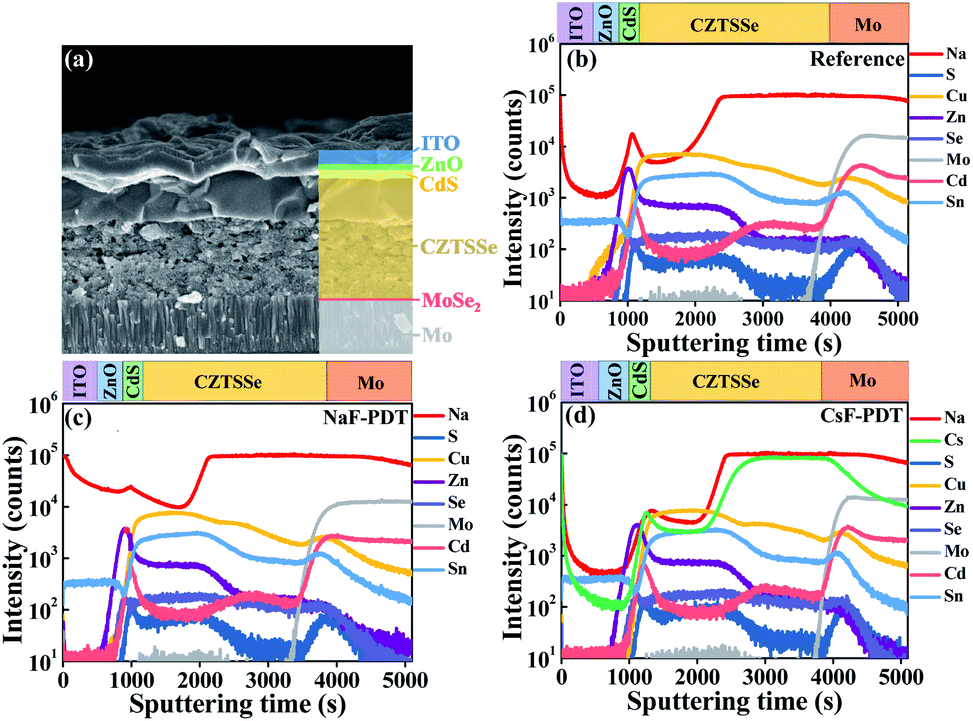 | ||
| Fig. 2 (a) SEM cross-section image of CZTSSe solar cells. SIMS depth profiles of (b) reference, (c) NaF-PDT and (d) CsF-PDT CZTSSe devices. | ||
To better elucidate the different functional mechanisms of light AMs and heavy AMs for the kesterite system, various bulk/GB analysis techniques were systematically employed to evaluate the structural and electrical properties evolution after the PDT process. Fig. 3 provides the capacitance–voltage (C–V) curves and derived free carrier density (NC–V) according to the following equation:50
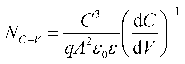 | (1) |
 | (2) |
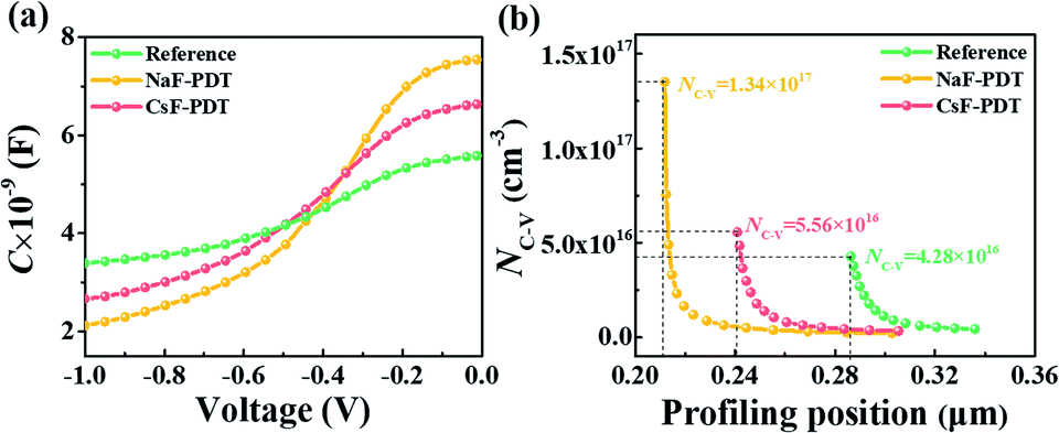 | ||
| Fig. 3 (a) C–V curves and (b) extracted carrier concentration of the reference, NaF-PDT and CsF-PDT CZTSSe devices. The data was measured at room temperature with in bias range of −1 to 0 V. | ||
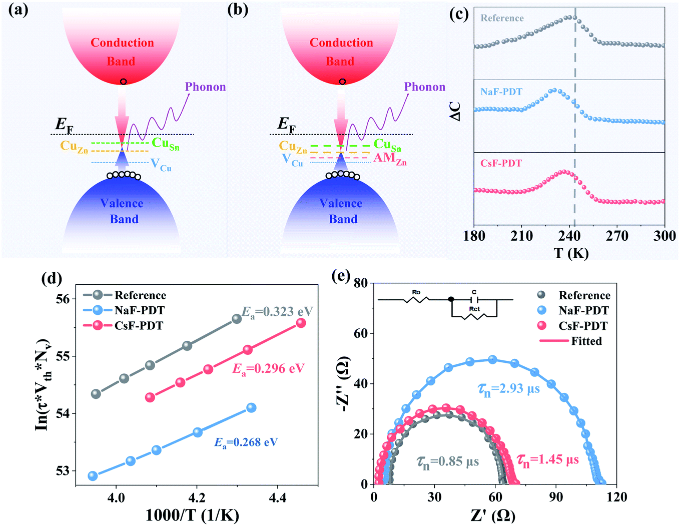 | ||
| Fig. 4 Formed major acceptor defects within CZTSSe absorber (a) before and (b) after AM-PDT. The sparse and dense dashed line (b) implies the decrease in CuZn and CuSn defects and increase in VCu in AM-PDT absorber, respectively. (c) C-DLTS Arrhenius curves, (d) extracted Ea and (e) EIS Nyquist plots of the reference, NaF-PDT, and CsF-PDT CZTSSe solar cells. | ||
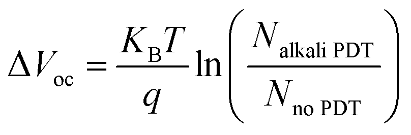
The detailed chemistry environment variation in the bulk absorber after the incorporation of AMs was analyzed by deep-level transient spectroscopy (C-DLTS),53 as seen in Fig. 4c and d. The defect activation energy (Ea), which plays a decisive role in carrier emission, minority carrier lifetime and majority carrier mobility, can be extracted from the Arrhenius plot.54 Due to the occupation of the Cu sites by the AM atoms in the kesterite lattice, it can be observed that the Ea decreased for the NaF-PDT and CsF-PDT devices. The lowest value of 0.268 eV implies that Na element with a smaller ionic radius is more effective to passivate the Cu-related deep level defects in the bulk absorber (Fig. 4a and b). According to eqn (2), the relation between Ea and carrier emission rate (Remission) can be expressed as:37
 | (3) |
The specific carrier recombination process for the CZTSSe solar cells before and after AM-PDT was characterized by electrochemistry impedance spectroscopy (EIS). Fig. 4e presents the measured Nyquist plots and the corresponding equivalent circuit composed of a junction capacitance (Cμ), recombination resistance (Rct), and series resistance (R0). Due to the high n-type doping on the CdS side of the CZTSSe/CdS mutation heterojunction, the depletion region is restricted on the absorber side. Therefore, the RC response of the carrier lifetime (τ = Rct × Cμ) is mainly the reflection of the charge recombination behavior in this region close to the p–n junction.55 After the incorporated of AMs into the kesterite system, the carrier lifetime was prolonged from 0.85 μs to 2.93 μs and 1.45 μs for the NaF-PDT and CsF-PDT systems, respectively. Ultimately, the accelerated carrier emission and depressed recombination processes in the CZTSSe:Na device contributed to the improved Voc and Jsc.
Furthermore, as a polycrystalline material, the oriented GBs are important current channels for electron or hole collection within CZTSSe thin films.56 Unfortunately, much more deep-level defects and dangling bonds with a lower formation energy are generated in this area, which become non-radiative recombination centers and deteriorate the device performance.9,11 GB passivation is essential for chalcogenide photovoltaics, and the electrical benefits of AMs have promoted every achievement of record efficiencies for CIGS PV in this aspect.57 Herein, the distinction of the different effects of Na and Cs atoms on the GB potential modification for CZTSSe solar cells was also identified by Kelvin probe force microscopy (KPFM) measurement. Fig. 5a–g and S13† show the topography, potential images and the extracted contact potential difference (CPD) across the GBs of the untreated, NaF-PDT and CsF-PDT CZTSSe films. The one-to-one correspondence within the topographic and potential images demonstrates the formation of a higher GB potential than that of GI for all three samples. As illustrated in Fig. 5h, the higher GB potential suggests the aggregation of electrons around the GBs and corresponds to downward band bending, which is often presented in the most efficient CZTSSe devices.56,58,59 Electrons and holes will severally transport along the GBs and GI before arriving at their respective electrode.52 After NaF-PDT and CsF-PDT, the CPD of the CZTSSe films is remarkably increased from ∼29 mV to ∼52 mV and ∼80 mV, respectively. This electric field polarity enhancement can be ascribed to the formation of surface dipoles (or (AMxCu1−x)2ZnSn(S,Se)4 compounds) and saturation of dangling bonds, thus reducing the work function and facilitating carrier separation. Meanwhile, the highest CPD variation of the CsF-PDT CZTSSe films also demonstrate the fact that the Cs atoms are superior to passivate GBs than Na atoms, which accelerated the charge transport and collection process, and thus improved the Jsc36 and FF59 by decreasing Rs.
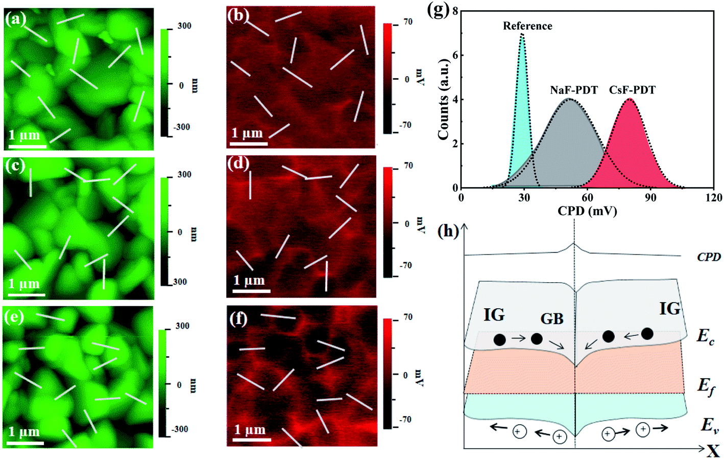 | ||
| Fig. 5 (a), (c), (e), (b), (d) and (f) are the surface topography and potential images of the reference, NaF-PDT, and CsF-PDT CZTSSe absorbers, respectively. (g) CPD statistical distributions derived from 10 denoted sites in (a)–(f) for each sample. (h) Schematic diagram of the band bending and contact potential difference near the GBs of the CZTSSe absorber. | ||
The intrinsic origination of the above distinct electrical effects of the Na and Cs atoms at localized GI and GBs may be mainly determined by their independent microscopic distribution within the absorber. Fig. 6 presents the scanning transmission electron microscopy (STEM) images of the cross-section of the absorber, enlarged GB morphology and relative AM element distribution profiles around the GBs for the NaF-PDT and Cs-PDT CZTSSe films. Due to the Cu-vacancy-mediated mass transport mechanism (e.g., NaCu → VCu) and the lower formation energy of the point defects at the GBs for all the alkali metal atoms, their diffusion paths within the bulk absorber can be divided into two routes of along the GBs and near the GBs. Meanwhile, their migration barrier increased with an increase in atom size. The smallest size of the Na atoms makes it feasible for them to jump back and forth between the GI and GBs. It can be observed that the concentration degree of Na remained at the same level for the GI and GBs sites or sometimes accompanied with a slight enrichment around the GBs within both samples. This gives a clear evidence that the Na atoms are randomly dispersed both in the GI and GBs, and the additional Na signal in the Cs-PDT films originated from the diffused Na ions within the soda-lime glass. On the other hand, the higher migration barrier makes Cs atoms difficult to diffuse from the GBs to GI, and the formed Cs-related defects are more thermodynamically stable than the Na-based defects at the GBs.47,60 The observed relative low signal within the GI and evident high signal around the GBs for the Cs element in the Cs-PDT films indicate that the Cs atoms are primarily segregated along the GBs with only a trace amount left in the interior grain.
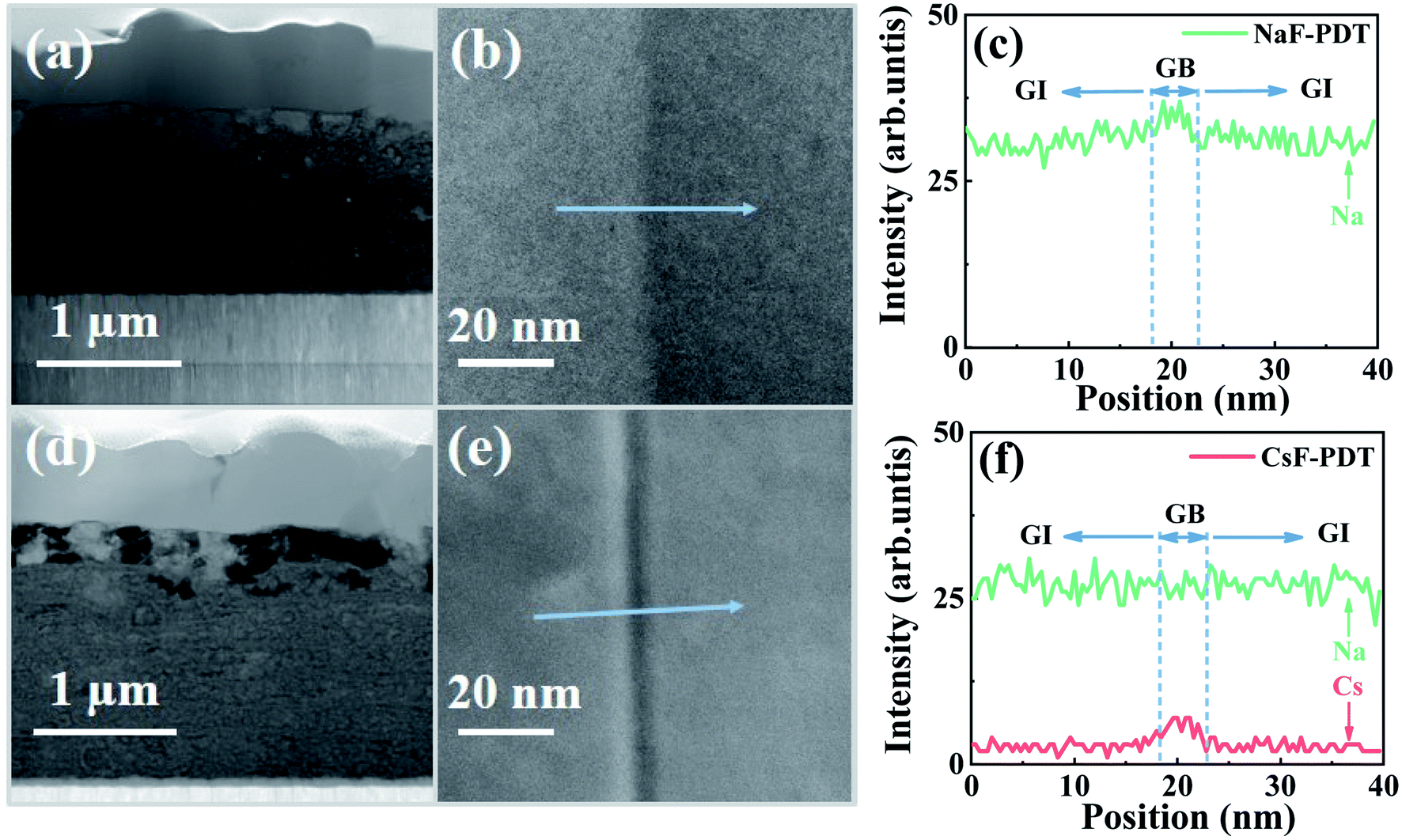 | ||
| Fig. 6 (a)–(c) and (d)–(f) STEM cross-section images, enlarged GB images and extracted alkali element distribution profiles across selected GBs of the NaF-PDT and CsF-PDT CZTSSe absorbers, respectively. | ||
Therefore, based on their distinct distribution and electric properties in kesterite photovoltaics, a plausible functional mechanism for the different types of AMs was proposed. The light AM atoms are randomly dispersed both in the GI and GBs (Fig. 7a), significantly increasing the acceptor concentration and passivating the deep level defects to enhance the Voc (especially for Na). In contrast the heavy AM atoms are mainly segregated at the GBs (Fig. 7b), primarily accelerating carrier transport and reducing the series resistance Rs to improve the FF. Considering the relative development in CIGS systems, if the specific electric benefits of light AMs and heavy AMs in the GI and GBs can also take effect independently, the key issues of Voc and FF hindering the continuous breakthrough of kesterite photovoltaics may be overcome. Thus, based on this assumption, the synergistic incorporation of additional Na and Cs atoms into the kesterite absorber was attempted.
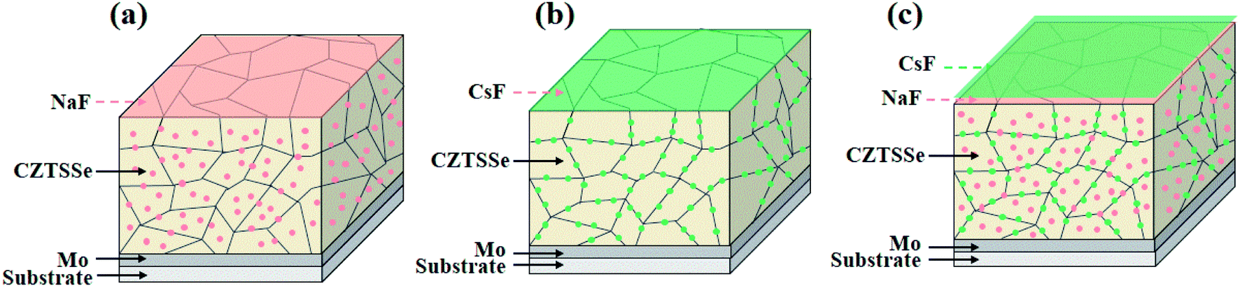 | ||
| Fig. 7 (a)–(c) Schematic diagrams of the alkali element distribution within the Na, Cs, and Na–Cs incorporated CZTSSe absorber. The pink and green dots stand for Na and Cs atoms, respectively. | ||
Specifically, 5 nm NaF-PDT and 5 nm CsF-PDT treatment was successively executed on the CZTSSe absorber. As illustrated in Fig. 7c, the Cs atoms occupy the Na atoms sites at the GBs via the Na–Cs ion-exchange mechanism.26 A concentrated Na concentration in the interior grain and segregated Cs atoms at the GBs were obtained and a portion of Na atoms diffused out of the absorber during the temperature cooling period.15Fig. 8a–c present the SIMS depth profiles throughout the absorber and local alkali element distribution across the selected GB of the Na–Cs synergistically incorporated CZTSSe solar cells. In comparison to the sole NaF-PDT and sole CsF-PDT devices, it can be observed that the Na content was reduced, while the Cs content increased both in the bulk absorber and along the GBs. Since the generated thermodynamically stable CsCu defect is electrically inactive, the hole concentration would even be decreased in comparison to that of the sole NaF-PDT device (Fig. 8d).
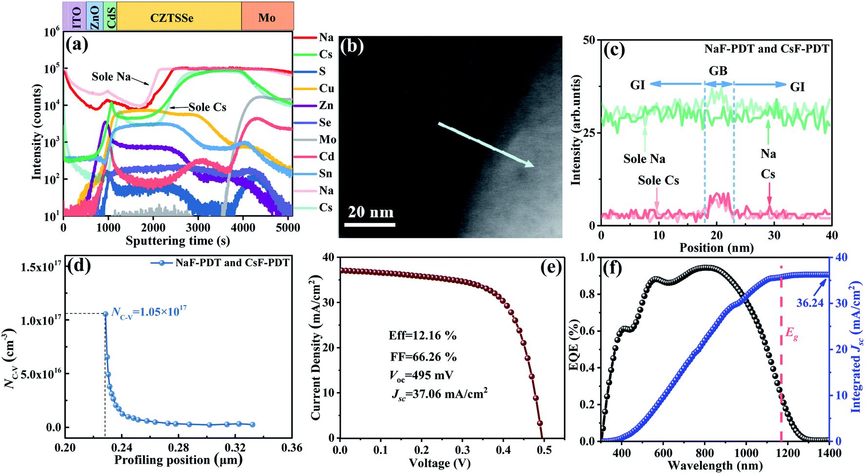 | ||
| Fig. 8 (a)–(f) SIMS depth profiles, enlarged STEM GB image, alkali element distribution profile across the GB, extracted carrier concentration, J–V curve and external quantum efficiency of Na–Cs synergistically incorporated CZTSSe solar cells, respectively. | ||
Accordingly, Fig. 8e and f show the best J–V curve and corresponding external quantum efficiency (EQE) of the Na–Cs synergistic incorporated CZTSSe solar cells. It can be found that this device generally possessed the optimal band gap of around 1.06 eV for efficient PV devices and its integral current matches well with the detected Jsc. Due to the prominent electric benefits of Cs at the GBs and Na in the GI, the device efficiency was further increased from 10.12% to 12.16% with Voc = 495 mV, FF = 66.26% and Jsc = 37.07 mA cm−2. Both the Voc and PCE are higher than that of the independent NaF or CsF-PDT device, demonstrating that the Na–Cs synergistic benefits take effect very well. This is the first time dual AM-PDT has been conducted in the kesterite system, and the photovoltaic parameters are all close to that of the IBM record cells, further supporting the aspect that the synergistic incorporation of Na and Cs should have great potential for future continuous breakthrough of high efficiency research. However, it should be noted that the obtained Voc is still much lower than that of the IBM record cell,14 which may be ascribed to the presence of a resistive fine-grain bottom layer61 and smaller optimal band gap (S/(S + Se) ratio) of our amine-thiol solution system. Thus, part of our future work will be focused on the improvement of these two aspects.
4. Conclusions
In summary, we proposed an Na–Cs dual alkali metal synergistic PDT route to overcome the key issues of Voc and FF hindering the continuous breakthrough of kesterite photovoltaics. This strategy was conducted by successively executing 5 nm NaF-PDT and 5 nm CsF-PDT treatments onto a CZTSSe absorber. The distinct distribution and electric benefits of the Na and Cs atoms were characterized by STEM, C–V, DLTS, and KPFM measurements. The experimental results proved that the light AMs and heavy AMs present different functional mechanisms in the kesterite system. The Na atoms are randomly dispersed in both the GI and GBs, significantly increasing the acceptor concentration and passivating the deep level defects to enhance the Voc (especially for Na). In contrast, the Cs atoms are mainly segregated at the GBs, primarily increasing the GB potential and improving the FF. Due to the prominent electric benefits of Cs at the GBs and Na in the GI, the device efficiency finally increased from 10.12% to 12.16% with Voc = 495 mV, FF = 66.26% and Jsc = 37.07 mA cm−2. The Na–Cs synergistic-assisted engineering of the acceptor concentration, deep level defects and GB potential in both the GBs and GI should have great promotion for the future development of kesterite photovoltaics.Conflicts of interest
The authors declare no competing financial interest.Acknowledgements
This work is supported by the National Natural Science Foundation of China (61874159, 62074052, 61974173, 51702085, 51802081 and 21603058), the Joint Talent Cultivation Funds of NSFC-HN (U1704151 and U1904192), Zhongyuan Thousand Talents (Zhongyuan Scholars) Program of Henan Province (202101510004), and the Science and Technology Innovation Talents in Universities of Henan Province (21HASTIT023). Key Lab of Photovoltaic and Energy Conservation Materials, Chinese Academy of Sciences is also gratefully acknowledged by the authors.Notes and references
- A. H. Pinto, S. W. Shin, E. Isaac, T. R. Knutson, E. S. Aydil and R. L. Penn, J. Mater. Chem. A, 2017, 5, 23179–23189 RSC.
- K. Sun, J. Huang, C. Yan, A. Pu, F. Liu, H. Sun, X. Liu, Z. Fang, J. A. Stride, M. Green and X. Hao, Chem. Mater., 2018, 30, 4008–4016 CrossRef CAS.
- Z. Su, G. Liang, P. Fan, J. Luo, Z. Zheng, Z. Xie, W. Wang, S. Chen, J. Hu, Y. Wei, C. Yan, J. Huang, X. Hao and F. Liu, Adv. Mater., 2020, 32, e2000121 CrossRef PubMed.
- J. Fu, D. Kou, W. Zhou, Z. Zhou, S. Yuan, Y. Qi and S. Wu, J. Mater. Chem. A, 2020, 8, 22292–22301 RSC.
- S. Giraldo, Z. Jehl, M. Placidi, V. Izquierdo-Roca, A. Pérez-Rodríguez and E. Saucedo, Adv. Mater., 2019, 31, 1806692 CrossRef PubMed.
- D.-H. Son, S.-H. Kim, S.-Y. Kim, Y.-I. Kim, J.-H. Sim, S.-N. Park, D.-H. Jeon, D.-K. Hwang, S.-J. Sung, J.-K. Kang, K.-J. Yang and D.-H. Kim, J. Mater. Chem. A, 2019, 7, 25279–25289 RSC.
- M. Nakamura, K. Yamaguchi, Y. Kimoto, Y. Yasaki, T. Kato and H. Sugimoto, IEEE J. Photovolt., 2019, 9, 1863–1867 Search PubMed.
- S. Chen, A. Walsh, X. G. Gong and S. H. Wei, Adv. Mater., 2013, 25, 1522–1539 CrossRef CAS PubMed.
- C.-Y. Liu, Z.-M. Li, H.-Y. Gu, S.-Y. Chen, H. Xiang and X.-G. Gong, Adv. Energy Mater., 2017, 7, 1601457 CrossRef.
- S. Berman, G. Sai Gautam and E. A. Carter, ACS Sustainable Chem. Eng., 2019, 7, 5792–5800 CrossRef CAS.
- T. Gershon, B. Shin, N. Bojarczuk, M. Hopstaken, D. B. Mitzi and S. Guha, Adv. Energy Mater., 2015, 5, 1400849 CrossRef.
- J.-S. Park, S. Kim, S. N. Hood and A. Walsh, Appl. Phys. Lett., 2018, 113, 212103 CrossRef.
- W. Shockley and H. J. Queisser, J. Appl. Phys., 1961, 32, 510–519 CrossRef CAS.
- W. Wang, M. T. Winkler, O. Gunawan, T. Gokmen, T. K. Todorov, Y. Zhu and D. B. Mitzi, Adv. Energy Mater., 2014, 4, 1301465 CrossRef.
- Z.-K. Yuan, S. Chen, Y. Xie, J.-S. Park, H. Xiang, X.-G. Gong and S.-H. Wei, Adv. Energy Mater., 2016, 6, 1601191 CrossRef.
- T. Kato, J.-L. Wu, Y. Hirai, H. Sugimoto and V. Bermudez, IEEE J. Photovolt., 2018, 9, 325–330 Search PubMed.
- D. Colombara, K. Conley, M. Malitckaya, H.-P. Komsa and M. J. Puska, J. Mater. Chem. A, 2020, 8, 6471–6479 RSC.
- K. F. Tai, R. Kamada, T. Yagioka, T. Kato and H. Sugimoto, Jpn. J. Appl. Phys., 2017, 56, 08MC03 CrossRef.
- P. Jackson, R. Wuerz, D. Hariskos, E. Lotter, W. Witte and M. Powalla, Phys. Status Solidi RRL, 2016, 10, 583–586 CrossRef CAS.
- S. Ishizuka, N. Taguchi and P. J. Fons, J. Phys. Chem. C, 2019, 123, 17757–17764 CrossRef CAS.
- F. Pianezzi, P. Reinhard, A. Chirila, B. Bissig, S. Nishiwaki, S. Buecheler and A. N. Tiwari, Phys. Chem. Chem. Phys., 2014, 16, 8843–8851 RSC.
- I. Khatri, M. Sugiyama and T. Nakada, Prog. Photovolt: Res. Appl., 2017, 25, 871–877 CrossRef CAS.
- M. Raghuwanshi, E. Cadel, S. Duguay, L. Arzel, N. Barreau and P. Pareige, Prog. Photovolt: Res. Appl., 2017, 25, 367–375 CrossRef CAS.
- S.-H. Wei, S. B. Zhang and A. Zunger, J. Appl. Phys., 1999, 85, 7214–7218 CrossRef CAS.
- O. Donzel-Gargand, T. Thersleff, J. Keller, T. Törndahl, F. Larsson, E. Wallin, L. Stolt and M. Edoff, Prog. Photovolt: Res. Appl., 2018, 26, 730–739 CrossRef CAS.
- P. Reinhard, B. Bissig, F. Pianezzi, E. Avancini, H. Hagendorfer, D. Keller, P. Fuchs, M. Döbeli, C. Vigo, P. Crivelli, S. Nishiwaki, S. Buecheler and A. N. Tiwari, Chem. Mater., 2015, 27, 5755–5764 CrossRef CAS.
- A. Chirila, P. Reinhard, F. Pianezzi, P. Bloesch, A. R. Uhl, C. Fella, L. Kranz, D. Keller, C. Gretener, H. Hagendorfer, D. Jaeger, R. Erni, S. Nishiwaki, S. Buecheler and A. N. Tiwari, Nat. Mater., 2013, 12, 1107–1111 CrossRef CAS PubMed.
- N. Taguchi, S. Tanaka and S. Ishizuka, Appl. Phys. Lett., 2018, 113, 113903 CrossRef.
- S. Siebentritt, E. Avancini, M. Bär, J. Bombsch, E. Bourgeois, S. Buecheler, R. Carron, C. Castro, S. Duguay, R. Félix, E. Handick, D. Hariskos, V. Havu, P. Jackson, H. P. Komsa, T. Kunze, M. Malitckaya, R. Menozzi, M. Nesladek, N. Nicoara, M. Puska, M. Raghuwanshi, P. Pareige, S. Sadewasser, G. Sozzi, A. N. Tiwari, S. Ueda, A. Vilalta-Clemente, T. P. Weiss, F. Werner, R. G. Wilks, W. Witte and M. H. Wolter, Adv. Energy Mater., 2020, 10, 1903752 CrossRef CAS.
- E. Handick, P. Reinhard, R. G. Wilks, F. Pianezzi, T. Kunze, D. Kreikemeyer-Lorenzo, L. Weinhardt, M. Blum, W. Yang, M. Gorgoi, E. Ikenaga, D. Gerlach, S. Ueda, Y. Yamashita, T. Chikyow, C. Heske, S. Buecheler, A. N. Tiwari and M. Bar, ACS Appl. Mater. Interfaces, 2017, 9, 3581–3589 CrossRef CAS PubMed.
- T.-Y. Lin, I. Khatri, J. Matsuura, K. Shudo, W.-C. Huang, M. Sugiyama, C.-H. Lai and T. Nakada, Nano Energy, 2020, 68, 104299 CrossRef CAS.
- E. Handick, P. Reinhard, J.-H. Alsmeier, L. Köhler, F. Pianezzi, S. Krause, M. Gorgoi, E. Ikenaga, N. Koch, R. G. Wilks, S. Buecheler, A. N. Tiwari and M. Bär, ACS Appl. Mater. Interfaces, 2015, 7, 27414–27420 CrossRef CAS PubMed.
- G. Altamura, M. Wang and K. L. Choy, Sci. Rep., 2016, 6, 22109 CrossRef CAS PubMed.
- D. Tiwari, M. Cattelan, R. L. Harniman, A. Sarua, N. Fox, T. Koehler, R. Klenk and D. J. Fermin, ACS Energy Lett., 2018, 3, 2977–2982 CrossRef CAS.
- Z. Tong, F. Liu, L. Jiang and Y. Lai, Mater. Lett., 2019, 254, 50–53 CrossRef CAS.
- C. M. Sutter-Fella, J. A. Stückelberger, H. Hagendorfer, F. La Mattina, L. Kranz, S. Nishiwaki, A. R. Uhl, Y. E. Romanyuk and A. N. Tiwari, Chem. Mater., 2014, 26, 1420–1425 CrossRef CAS.
- Y.-R. Lin, V. Tunuguntla, S.-Y. Wei, W.-C. Chen, D. Wong, C.-H. Lai, L.-K. Liu, L.-C. Chen and K.-H. Chen, Nano Energy, 2015, 16, 438–445 CrossRef CAS.
- B. Duan, L. Guo, Q. Yu, J. Shi, H. Wu, Y. Luo, D. Li, S. Wu, Z. Zheng and Q. Meng, J. Energy Chem., 2020, 40, 196–203 CrossRef.
- A. Cabas-Vidani, S. G. Haass, C. Andres, R. Caballero, R. Figi, C. Schreiner, J. A. Márquez, C. Hages, T. Unold, D. Bleiner, A. N. Tiwari and Y. E. Romanyuk, Adv. Energy Mater., 2018, 8, 1801191 CrossRef.
- H. Xin, S. Vorpahl, A. Collord, I. Braly, A. Uhl, B. Krueger, D. Ginger and H. Hillhouse, Phys. Chem. Chem. Phys., 2015, 17, 23859–23866 RSC.
- S. G. Haass, C. Andres, R. Figi, C. Schreiner, M. Bürki, Y. E. Romanyuk and A. N. Tiwari, Adv. Energy Mater., 2018, 8, 1701760 CrossRef.
- Z.-K. Yuan, S. Chen, H. Xiang, X.-G. Gong, A. Walsh, J.-S. Park, I. Repins and S.-H. Wei, Adv. Funct. Mater., 2015, 25, 6733–6743 CrossRef CAS.
- Y.-T. Hsieh, Q. Han, C. Jiang, T.-B. Song, H. Chen, L. Meng, H. Zhou and Y. Yang, Adv. Energy Mater., 2016, 6, 1502386 CrossRef.
- A. Mule, B. Vermang, M. Sylvester, G. Brammertz, S. Ranjbar, T. Schnabel, N. Gampa, M. Meuris and J. Poortmans, Thin Solid Films, 2017, 633, 156–161 CrossRef CAS.
- P. M. P. Salomé, H. Rodriguez-Alvarez and S. Sadewasser, Sol. Energy Mater. Sol. Cells, 2015, 143, 9–20 CrossRef.
- Y. Sun, S. Lin, W. Li, S. Cheng, Y. Zhang, Y. Liu and W. Liu, Engineering, 2017, 3, 452–459 CrossRef CAS.
- T. Maeda, A. Kawabata and T. Wada, Phys. Status Solidi C, 2015, 12, 631–637 CrossRef CAS.
- A. Davydova, K. Rudisch and J. J. Scragg, Chem. Mater., 2018, 30, 4624–4638 CrossRef CAS.
- A. Chirilă, P. Reinhard, F. Pianezzi, P. Bloesch, A. R. Uhl, C. Fella, L. Kranz, D. Keller, C. Gretener and H. Hagendorfer, Nat. Mater., 2013, 12, 1107–1111 CrossRef PubMed.
- X. Zhao, D. Kou, W. Zhou, Z. Zhou, Y. Meng, Q. Meng, Z. Zheng and S. Wu, J. Mater. Chem. A, 2019, 7, 3135–3142 RSC.
- K. Tse, M. Wong, Y. Zhang, J. Zhang, M. Scarpulla and J. Zhu, J. Appl. Phys., 2018, 124, 165701 CrossRef.
- M. Han, X. Zhang and Z. Zeng, Phys. Chem. Chem. Phys., 2017, 19, 17799–17804 RSC.
- Y. Qi, D. Kou, W. Zhou, Z. Zhou, Q. Tian, Y. Meng, X. Liu, Z. Du and S. Wu, Energy Environ. Sci., 2017, 10, 2401–2410 RSC.
- X. Zhao, X. Chang, D. Kou, W. Zhou, Z. Zhou, Q. Tian, S. Yuan, Y. Qi and S. Wu, J. Energy Chem., 2020, 50, 9–15 CrossRef.
- Y. Zhao, S. Yuan, D. Kou, Z. Zhou, X. Wang, H. Xiao, Y. Deng, C. Cui, Q. Chang and S. Wu, ACS Appl. Mater. Interfaces, 2020, 12, 12717–12726 CrossRef PubMed.
- J. B. Li, V. Chawla and B. M. Clemens, Adv. Mater., 2012, 24, 720–723 CrossRef CAS PubMed.
- N. Nicoara, R. Manaligod, P. Jackson, D. Hariskos, W. Witte, G. Sozzi, R. Menozzi and S. Sadewasser, Nat. Commun., 2019, 10, 3980 CrossRef PubMed.
- H. Guo, G. Wang, R. Meng, Y. Sun, S. Wang, S. Zhang, J. Wu, L. Wu, G. Liang, H. Li and Y. Zhang, J. Mater. Chem. A, 2020, 8, 22065–22074 RSC.
- J. Kim, G. Y. Kim, D.-H. Son, K.-J. Yang, D.-H. Kim, J.-K. Kang and W. Jo, Sol. Energy Mater. Sol. Cells, 2018, 183, 129–136 CrossRef CAS.
- M. Chugh, T. D. Kuhne and H. Mirhosseini, ACS Appl. Mater. Interfaces, 2019, 11, 14821–14829 CrossRef CAS PubMed.
- X. Liu, J. Huang, F. Zhou, F. Liu, K. Sun, C. Yan, J. A. Stride and X. Hao, Chem. Mater., 2016, 28, 3649–3658 CrossRef CAS.
Footnotes |
| † Electronic supplementary information (ESI) available. See DOI: 10.1039/d0ta08224d |
| ‡ Xiaohuan Chang and Junjie Fu contributed equally to this work. |
| This journal is © The Royal Society of Chemistry 2021 |