
Layered cobalt oxide epitaxial films exhibiting thermoelectric ZT = 0.11 at room temperature†
Yugo
Takashima
a,
Yu-qiao
Zhang
 *b,
Jiake
Wei
cd,
Bin
Feng
c,
Yuichi
Ikuhara
cd,
Hai Jun
Cho
ab and
Hiromichi
Ohta
*ab
*b,
Jiake
Wei
cd,
Bin
Feng
c,
Yuichi
Ikuhara
cd,
Hai Jun
Cho
ab and
Hiromichi
Ohta
*ab
aGraduate School of Information Science and Technology, Hokkaido University, N14W9, Kita, Sapporo 060-0814, Japan. E-mail: hiromichi.ohta@es.hokudai.ac.jp
bResearch Institute for Electronic Science, Hokkaido University, N20W10, Kita, Sapporo 001-0020, Japan. E-mail: yuqiaozhang0730@gmail.com
cInstitute of Engineering Innovation, The University of Tokyo, 2-11-16 Yayoi, Bunkyo, Tokyo 113-8656, Japan
dElements Strategy Initiative for Structural Materials, Kyoto University, Yoshida-honmachi, Sakyo-ku, Kyoto 606-8501, Japan
First published on 13th October 2020
Abstract
Among many thermoelectric materials, oxide-based materials draw significant interest due to their environmental compatibility. In particular, layered cobaltite, Na0.75CoO2, shows a large thermoelectric power factor parallel to the layers. However, the thermal conductivity (κ) is rather high (5–7 W m−1 K−1), and therefore, its thermoelectric figure of merit ZT is small (∼0.03) at room temperature. Here we show that substituting the Na+ ion with the Ba2+ ion in NaxCoO2 drastically reduces the κ while keeping the large power factor, resulting in a large enhancement in ZT. We fabricated epitaxial films of Na0.75CoO2 by the reactive solid-phase epitaxy method and performed ion-exchange treatment from Na+ to Ba2+ to synthesize Ba0.27CoO2 films. The room temperature electrical conductivity (σ), thermopower (S), and power factor of the c-axis oriented Ba0.27CoO2 films along the in-plane direction were 2310 S cm−1, +72 μV K−1, and 1.2 mW m−1 K−2, respectively, while the κ along the in-plane, which was clarified by measuring the κ of the c-axis inclined (55°) film, was 3.3 W m−1 K−1. This yields a ZT (= S2σT/κ) value along the in-plane as high as 0.11 at room temperature, which is the highest among those reported for oxide thermoelectric materials except oxychalcogenide (BiO)(CuSe).
Introduction
Thermoelectric devices convert a temperature difference into electric current and vice versa, from the Seebeck effect/Peltier effect.1,2 Since thermoelectric devices can convert wasted heat exhausted in our daily life into electricity, they have attracted increasing attention as a potential solution for the realization of affordable and clean energy in Sustainable Development Goals (SDGs).3,4 Previously, wasted heat from large-scale high-temperature environments, like factories, thermal power plants, and automobiles, has been targeted for thermoelectric conversion. Therefore, thermoelectric materials exhibiting a large figure of merit (ZT) at high-temperature (800–1000 K) have been developed proactively.5–8 Nevertheless, thermoelectric conversion of small-scale exhausted heat from computers, stoves, sunlight, and our body is also important for the realization of SDGs. Thus, thermoelectric materials exhibiting a large ZT around room temperature are also required.Further, thermoelectric materials must avoid the use of rare and toxic elements since economic and environmental viabilities are of great concern in future. Therefore, although layered bismuth telluride based thermoelectric materials exhibit large ZT (= S2σT/κ = ∼0.8,1 where S, σ, T, and κ are the thermopower, electrical conductivity, absolute temperature, and thermal conductivity) values at room temperature, they lack the sustainability due to the existence of Te, which is rare and toxic. In this regard, oxide-based thermoelectric materials offer an excellent alternative due to their environmental compatibility.9 Although it is known that oxychalcogenide (BiO)(CuSe)10,11 exhibits a large ZT ∼ 0.2 at room temperature and ∼1.4 at 650 °C, chemical instability under an oxygen atmosphere at high temperature can potentially cause problems in real application. Two of the most commonly used thermoelectric oxides, electron-doped SrTiO3 and Ca3Co4O9, exhibit large ZT values at elevated temperatures (ZT ∼ 0.3 at 1000 K as the reliable value).12,13 However, the ZT values of these oxides are extremely small at room temperature (ZT ∼ 0.05 for electron doped SrTiO3 and ZT ∼ 0.04 for Ca3Co4O9).12 The origin of such low ZT observed from oxides at room temperature is their high κ. For example, Na0.75CoO2 shows a large thermoelectric power factor (PF = S2σ, 2.38 mW m−1 K−2) along the layers.14 However, the κ is rather high (∼7 W m−1 K−1), and therefore, the thermoelectric figure of merit ZT is small (∼0.03 (ref. 15 and 16)) at room temperature.
In order to overcome this difficulty, we recently investigated the effect of ion exchange from the Na+ ion to alkali earth ions on the κ of Na0.75CoO2.17 Firstly, we fabricated Na0.75CoO2 epitaxial films by the reactive solid-phase (R-SPE) epitaxy method.18–20 Then, the Na+ ions were topotactically substituted with Ca2+ and Sr2+ ions by the conventional ion exchange treatment.21–23 We measured the κ of the resultant epitaxial films of Na0.75CoO2, Ca1/3CoO2, and Sr1/3CoO2 using the time-domain thermoreflectance (TDTR) method, and the result showed that the κ parallel to this layered structure can be reduced by substituting heavier elements between the CoO2 planes, as schematically hypothesized in Fig. 1, whereas the κ normal to the layered structure was ∼1.5 W m−1 K−1, independent of the element mass.17
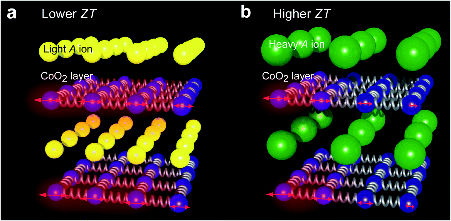 | ||
| Fig. 1 Hypothesis toward the ZT improvement of layered cobaltite, AxCoO2. We expected that the lattice vibration, indicated by red arrows of the rigid CoO2 layer would be significantly suppressed by the substitution of the A ion from (a) light one to (b) heavy one. If the substitution does not affect the power factor (S2σ), the ZT would be improved significantly by the substitution. | ||
In this study, we focused on the substitution of Ba2+ because the atomic mass of Ba is the heaviest among alkali earth elements. The thermoelectric properties of Ba1/3CoO2 were addressed in a few previous studies. Recently, Liu et al. fabricated BaxCoO2 (x = 0.19, 0.28, 0.30, and 0.33) ceramic samples through the ion-exchange treatment of NaxCoO2 ceramics and measured the thermoelectric properties.24,25 They showed that the resistivity (ρ), S, and κ of the BaxCoO2 ceramics at room temperature were 4–30 mΩ cm (σ = 33–250 S cm−1), ∼+70 μV K−1, and 3–5 W m−1 K−1, respectively. Thus, the ZT of the BaxCoO2 ceramics at room temperature was 0.012 at the largest. The PF was 0.12 mW m−1 K−2, which is an order of magnitude lower than that of the epitaxial films of Na0.75CoO2 (1.23 mW m−1 K−2), Ca1/3CoO2 (1.08 mW m−1 K−2), and Sr1/3CoO2 (1.18 mW m−1 K−2), measured parallel to the layered structure,17 which is probably due to carrier scattering at grain or domain boundaries. On the other hand, the lowest κ was 3 W m−1 K−1, which is lower than that of the epitaxial films of Na0.75CoO2 (5.46 W m−1 K−1), Ca1/3CoO2 (6.79 W m−1 K−1), and Sr1/3CoO2 (4.51 W m−1 K−1) (parallel to the layered structure).17 From these points of view, we expected that Ba1/3CoO2 epitaxial films show an enhanced ZT parallel to the layered structure as their power factor is not significantly damaged by grain or domain boundaries.
Here we report that the Ba1/3CoO2 epitaxial films, which were fabricated by the ion exchange treatment of Na0.75CoO2 epitaxial films, exhibit significantly low κ while maintaining the large power factor and show rather large ZT = 0.11 at room temperature. This value is the highest among those reported for oxide thermoelectric materials except oxychalcogenide (BiO)(CuSe).
Experimental
Preparation of Na0.75CoO2 epitaxial films
We prepared Ba1/3CoO2 epitaxial films as schematically summarized in Fig. 2, which also shows the crystal structures of CoO, Na0.75CoO2, and Ba1/3CoO2. Na0.75CoO2 epitaxial films were prepared on α-Al2O3 substrates by the reactive solid-phase epitaxy (R-SPE) method.18–20 First, CoO films were heteroepitaxially grown on (0001) or (1![[1 with combining macron]](https://www.rsc.org/images/entities/char_0031_0304.gif) 00) α-Al2O3 single-crystal substrates (10 mm × 10 mm × 0.5 mm) at 700 °C in an oxygen atmosphere (10−3 Pa) by the pulsed laser deposition technique (KrF excimer laser, ∼2 J cm−2 per pulse, 10 Hz). Then, the surface of the CoO film was heated at 750 °C in air with NaHCO3 powder. In order to keep the film surface clean, the yttria stabilized zirconia (YSZ) single crystal plate (10 mm × 10 mm × 0.5 mm) was put on the film surface during the heating. The detailed preparation process of Na0.75CoO2 epitaxial films is described elsewhere.18–20
00) α-Al2O3 single-crystal substrates (10 mm × 10 mm × 0.5 mm) at 700 °C in an oxygen atmosphere (10−3 Pa) by the pulsed laser deposition technique (KrF excimer laser, ∼2 J cm−2 per pulse, 10 Hz). Then, the surface of the CoO film was heated at 750 °C in air with NaHCO3 powder. In order to keep the film surface clean, the yttria stabilized zirconia (YSZ) single crystal plate (10 mm × 10 mm × 0.5 mm) was put on the film surface during the heating. The detailed preparation process of Na0.75CoO2 epitaxial films is described elsewhere.18–20
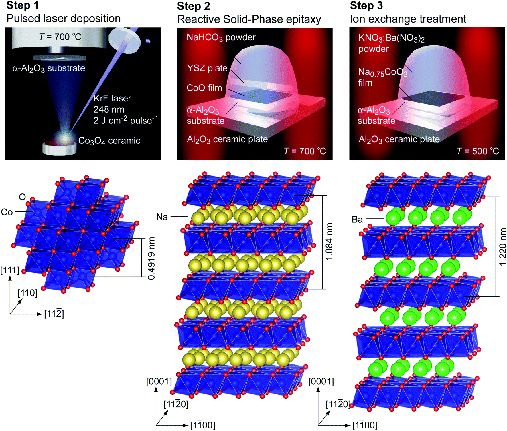 | ||
| Fig. 2 Fabrication procedure of Ba1/3CoO2 epitaxial films. Step 1: CoO epitaxial film growth by pulsed laser deposition on α-Al2O3 substrates. Step 2: Na0.75CoO2 film growth by the reactive solid-phase epitaxy method. Step 3: Ion exchange treatment from Na to Ba. After the ion exchange treatment, the resultant film was washed with distilled water several times. | ||
Ion exchange from Na+ to Ba2+
The ion exchange from Na+ to Ba2+ was performed by heating the Na0.75CoO2 epitaxial films with molten Ba(NO3)2 and KNO3 at 500 °C in an alumina crucible for 1 h. After the ion exchange treatment, the resultant films were washed with distilled water. These processes were similar to the process used to prepare Sr1/3CoO2 and Ca1/3CoO2 epitaxial films by the ion exchange of Na0.75CoO2 epitaxial films.22,23Crystallographic characterization of the films
Crystallographic characteristics including the thickness, orientation, and lattice parameters of the resultant films were analyzed using high-resolution X-ray diffraction (HR-XRD, Cu Kα1 radiation, ATX-G, Rigaku Co.). Out-of-plane Bragg diffraction patterns, in-plane Bragg diffraction patterns, rocking curves, and X-ray reflection patterns were acquired. The surface morphologies of the resultant films were observed with a scanning probe microscope (SPM, Nanocute, Hitach High-Tech Sci. Co.). Topographic atomic force microscopy (AFM) images (2 μm × 2 μm) were acquired. The atomic arrangement of the resultant films was visualized using a high-angle annular dark-field scanning transmission electron microscope (HAADF-STEM).Measurements of the electrical conductivity and thermopower
The electrical conductivity of the resultant films was measured by the dc four-probe method in the van der Pauw electrode configuration. The thermopower of the resultant films was measured by the conventional steady-state method. The film sample was placed on the gap (∼5 mm) between two Peltier devices. By applying the forward/reverse current to each Peltier device, temperature differences were generated in the sample. We then measured the temperature difference (ΔT) and the thermo-electromotive force (ΔV) simultaneously at room temperature, and the thermopower was calculated as the linear slope of the ΔT − ΔV plot (ESI Fig. S1†). Details of our thermopower measurement system are described elsewhere.26,27Measurements of the thermal conductivity
Cross-plane thermal conductivity (κ) of the resultant films was measured by time domain thermo-reflectance (TDTR, PicoTR, PicoTherm Co.). 116 nm-thick Mo was deposited on the resultant films as a transducer by dc sputtering. The decay curves of the TDTR signals were simulated using the packaged software developed by PicoTherm Co. In our simulation, to minimize the number of free parameters, we used constant values for Mo transducers, including bulk density = 10![[thin space (1/6-em)]](https://www.rsc.org/images/entities/char_2009.gif) 000 kg m−3, heat capacity (Cp) = 250 J kg−1 K−1 and κ = 45.4 W m−1 K−1. Details of our thermal conductivity measurement system are described elsewhere.17,28,29
000 kg m−3, heat capacity (Cp) = 250 J kg−1 K−1 and κ = 45.4 W m−1 K−1. Details of our thermal conductivity measurement system are described elsewhere.17,28,29
Uncertainty in the ZT value
We fabricated more than 5 samples and we measured all samples. The uncertainty in the S and the σ was less than 5%, while that in the κ was ∼15%. Therefore, the uncertainty in the ZT is approximated to be ∼20%.Results and discussion
Fig. 3 summarizes the out-of-plane XRD patterns and the topographic atomic force microscopy (AFM) images of the resultant CoO film (Fig. 3a and d), R-SPE grown Na0.75CoO2 film (Fig. 3b and e), and Ba2+ ion-exchanged film (Fig. 3c and f) grown on (0001) α-Al2O3 substrates. Only an intense Bragg peak of 111 CoO is seen together with the 0006 α-Al2O3 substrate (Fig. 3a), indicating strong (111) orientation in the CoO film. The full width at half maximum (FWHM) of the out-of-plane rocking curve (OXRC) of 111 CoO was ∼0.02° (ESI Fig. S2a†), which is almost as small as the resolution of our optical setup of the XRD. The thickness of the CoO film was 93 nm, which was evaluated using the Pendellösung fringes around the Bragg peak of 111 CoO. The heteroepitaxial growth with the relationship of (111)[10] CoO‖(0001)[100] α-Al2O3 was confirmed by the in-plane XRD patterns (ESI Fig. S3a†). Triangle shaped facets are clearly seen in the topographic AFM image of the film (Fig. 3d), confirming the heteroepitaxial growth of CoO.
 | ||
| Fig. 3 Crystal structural analyses of the resultant films. (a)–(c) Change in the out-of-plane XRD pattern of the resultant films grown on the (0001) α-Al2O3 substrate (a) after step 1, (b) after step 2, and (c) after step 3. The crystalline phase of (a) is CoO (93 nm), (b) is Na0.75CoO2 (182 nm), and (c) is Ba1/3CoO2 (200 nm). (d)–(f) Topographic AFM images of the resultant films grown on the (0001) α-Al2O3 substrate (a) after step 1 (CoO), (b) after step 2 (Na0.75CoO2), and (c) after step 3 (Ba1/3CoO2). (g)–(i) Topographic AFM images of the resultant films grown on the (100) α-Al2O3 substrate (a) after step 1, (b) after step 2, and (c) after step 3. All the scale bars are 1 μm. Plate-like grains are seen in (d)–(f), whereas stripe patterns are seen in (g)–(i). | ||
After the R-SPE treatment, only intense Bragg peaks of 000l Na0.75CoO2 are seen (Fig. 3b). The thickness of the Na0.75CoO2 film was 182 nm, roughly twice that of the CoO film. Although the FWHM of the OXRC of 0002 Na0.75CoO2 was ∼0.6° (ESI Fig. S2b†), hexagonal-shaped plate-like crystals with large terraces were observed in the topographic AFM image (Fig. 3e). Thus, the broadening of the FWHM of the OXRC indicates the bending of the Na0.75CoO2 crystal. The in-plane XRD pattern (ESI Fig. S3b†) confirmed the heteroepitaxial growth of the Na0.75CoO2 film on the (0001) α-Al2O3 substrate with the epitaxial relationship of (0001)[11![[2 with combining macron]](https://www.rsc.org/images/entities/char_0032_0304.gif) 0] Na0.75CoO2‖(0001)[100] α-Al2O3. After the Ba2+ ion exchange treatment, the Bragg peak position of 000l is shifted to the left, indicating a lattice expansion in the out-of-plane direction (Fig. 3c). The c-axis lattice parameter is 12.225 Å, which corresponds well to the reported value (12.2 Å (ref. 25)) of Ba1/3CoO2. The in-plane XRD pattern (ESI Fig. S3c†) indicated that there are two ordered structures of Ba ions. The a-axis lattice parameter was calculated to be 2.829 Å. The topographic AFM image of the resultant film (Fig. 3f) is similar to that of the Na0.75CoO2 film.
0] Na0.75CoO2‖(0001)[100] α-Al2O3. After the Ba2+ ion exchange treatment, the Bragg peak position of 000l is shifted to the left, indicating a lattice expansion in the out-of-plane direction (Fig. 3c). The c-axis lattice parameter is 12.225 Å, which corresponds well to the reported value (12.2 Å (ref. 25)) of Ba1/3CoO2. The in-plane XRD pattern (ESI Fig. S3c†) indicated that there are two ordered structures of Ba ions. The a-axis lattice parameter was calculated to be 2.829 Å. The topographic AFM image of the resultant film (Fig. 3f) is similar to that of the Na0.75CoO2 film.
Since the orientation of the films was inclined on the (100) α-Al2O3 substrate, Bragg diffraction peaks were not observed in the out-of-plane Bragg patterns of the resultant CoO film, R-SPE grown Na0.75CoO2 film, and Ba2+ ion-exchanged film (data not shown). Fig. 3g–i show the topographic AFM images of the CoO (Fig. 3g), Na0.75CoO2 (Fig. 3h), and Ba2+ ion-exchanged (Fig. 3i) films grown on the (100) α-Al2O3 substrate in the same way. Stripe patterns are seen in Fig. 3g–i, which are similar to the surface of inclined films. The heteroepitaxial growth of CoO, Na0.75CoO2, and Ba1/3CoO2 films on the (100) α-Al2O3 substrate was confirmed by the in-plane XRD patterns (ESI Fig. S4†): [10] CoO‖[0001] α-Al2O3, [110] Na0.75CoO2‖[0001] α-Al2O3, and [110] Ba1/3CoO2‖[0001] α-Al2O3.
To further clarify the orientation of the film and the atomic arrangement, we performed high-angle annular dark-field scanning transmission electron microscopy (HAADF-STEM) observation. Fig. 4a and b show the cross-sectional HAADF-STEM images of the Ba2+ ion-exchanged films on the (0001) α-Al2O3 substrate. The e-beam incident direction is along the [100] α-Al2O3. The layered atomic arrangement parallel to the substrate surface is clearly visualized (Fig. 4b and ESI Fig. S5a†). An approximately 10 nm-thick amorphous layer is also detected between the layered crystal and the substrate. Energy dispersive X-ray spectroscopy (EDS) results of the film (data not shown) revealed that the upper part of the film is composed of Ba, Co, and O. The signal from Na was negligible. The bottom amorphous part is composed of Ba, Al, and O. The concentration ratio of Ba/Co inside the film was about 0.27. These results show that the resultant film is Ba0.27CoO2.
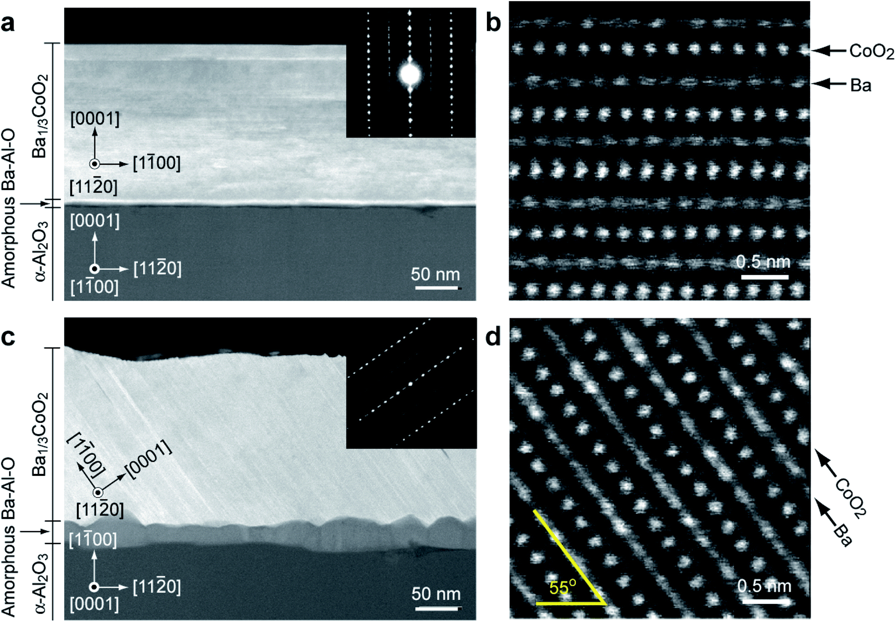 | ||
| Fig. 4 Cross-sectional atomic arrangement of the Ba1/3CoO2 films. (a) Cross-sectional HAADF-STEM image of the Ba1/3CoO2 epitaxial film grown on the (0001) α-Al2O3 substrate. The selected area electron diffraction pattern and (b) the magnified HAADF-STEM image reveals that Ba and CoO2 layers are stacked parallel to the substrate surface. (c) Cross-sectional HAADF-STEM image of the Ba1/3CoO2 epitaxial film grown on the (100) α-Al2O3 substrate. The selected area electron diffraction pattern and (d) the magnified HAADF-STEM image reveal that Ba and CoO2 layers are inclined 55° to the substrate surface. | ||
On the other hand, an inclined layered structure was revealed in the HAADF-STEM images of the film on the (100) α-Al2O3 substrate (Fig. 4c and d). The e-beam incident direction is along the [0001] α-Al2O3. Similar to the Ba0.27CoO2 film on the (0001) α-Al2O3 substrate, the layered atomic arrangement is clearly visualized. It should be noted that the layer is inclined 55° to the substrate surface. Although the interface amorphous layer is thick (15–30 nm), the crystal structure and the chemical composition of the layered crystal layer are similar to those of the Ba1/3CoO2 film on the (0001) α-Al2O3 substrate. The inclined structure is consistent with the topographic AFM image (Fig. 3i).
Then, we measured the electrical conductivity (σ) and thermopower (S) parallel to the film surface of the (0001)-oriented Ba0.27CoO2 film grown on the (0001) α-Al2O3 substrate at room temperature. The σ was 2310 S cm−1, the S was +72 μV K−1, and the power factor (PF = S2σ) was 1.2 mW m−1 K−2, respectively. The PF is the same (1.2 mW m−1 K−2) as that of the (0001)-oriented Na0.75CoO2 film grown on the (0001) α-Al2O3 substrate at room temperature. Thus, Ba ion substitution does not affect the PF.
Next, we measured the thermal conductivity (κ) normal to the film surface of the Ba0.27CoO2 films grown on (0001) and (100) α-Al2O3 substrates by the TDTR method at room temperature. The κ of the Ba0.27CoO2 film on the (0001) α-Al2O3 substrate was 1.3 W m−1 K−1 and that on the (100) α-Al2O3 substrate was 2.8 W m−1 K−1. In order to extract κ parallel to the layered structure in the Ba0.27CoO2 film, we used the following equation as reported previously.17

Here we summarize and compare the thermoelectric properties of the Ba0.27CoO2 and Na0.75CoO2 films on the (0001) α-Al2O3 substrate along with reported values for Ca1/3CoO2 and Sr1/3CoO2 (ref. 22 and 23) (Fig. 5 and ESI Table S1†). Although there are some differences in the in-plane electrical conductivity (σip) (Fig. 5a) and thermopower (Sip) (Fig. 5b) of Ca1/3CoO2, Na0.75CoO2, Sr1/3CoO2 and Ba0.27CoO2, the power factor PFip (Fig. 5c) is almost constant (1.08–1.2 mW m−1 K−2) and does not show clear dependence on the atomic mass of Ax. The main difference was detected in the thermal conductivity (κ) (Fig. 5d). Although the out-of-plane thermal conductivity (κop) was almost independent of the atomic mass of Ax, the κip drastically decreased from 6.79 W m−1 K−1 to 3.29 W m−1 K−1 with increasing the atomic mass of Ax from 13.2 (Ca1/3) to 45.3 (Ba1/3), resulting in a significant enhancement in ZT along the layered structure. The resulting ZTin was 0.11 at room temperature, which is the highest among those reported for oxide thermoelectric materials except oxychalcogenide (BiO)(CuSe).
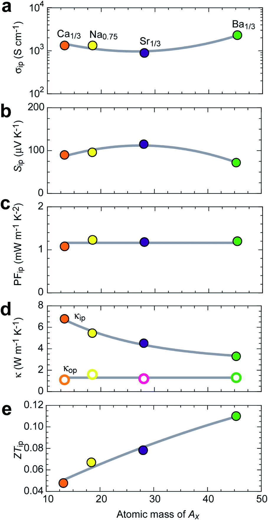 | ||
| Fig. 5 Thermoelectric properties of AxCoO2 epitaxial films at room temperature. (a) In-plane electrical conductivity (σip), (b) in-plane thermopower (Sip), (c) in-plane power factor (PFip), (d) in-plane and out-of-plane thermal conductivity (κip, κop), and (e) in-plane figure of merit (ZTip) as a function of the atomic mass of Ax in AxCoO2. The κip shows a clear decreasing tendency whereas the PF shows a slightly increasing tendency. These resulted in an increasing tendency of ZT. The ZT reached 0.11 when Ax = Ba1/3. | ||
Conclusions
In summary, we have shown that substitution of the Na+ ion with the Ba2+ ion in Na0.75CoO2 significantly reduces the in-plane κ while keeping the large power factor, resulting in a large enhancement of ZT. We fabricated the epitaxial films of Ba1/3CoO2 from Na0.75CoO2 epitaxial films by ion-exchange between Na+ and Ba2+. The σ, S, and power factor of the c-axis oriented Ba1/3CoO2 films along the in-plane were 2310 S cm−1, +72 μV K−1, and 1.2 mW m−1 K−2, respectively. The κ along the in-plane, which was clarified by measuring the κ of the c-axis inclined (55°) film, was 3.29 W m−1 K−1. The ZT along the in-plane was as large as 0.11 at room temperature, which is the highest among those reported for oxide thermoelectric materials except oxychalcogenide (BiO)(CuSe).Author contributions
Y. T. and Y. Z. performed the sample preparation, measurements, and analyses. J. W., B. F., and Y. I. performed the STEM analyses. H. J. C. analyzed and interpreted the data. H. O. planned and supervised the project. All authors discussed the results and commented on the manuscript.Conflicts of interest
There are no conflicts to declare.Acknowledgements
This research was supported by Grants-in-Aid for Innovative Areas (19H05791 and 19H05788) and Grants-in-Aid for Scientific Research A (17H01314) from the JSPS. A part of this work was supported by Dynamic Alliance for Open Innovation Bridging Human, Environment, and Materials, and by the Network Joint Research Center for Materials and Devices. A part of this work was conducted at the Advanced Characterization Nanotechnology Platform of the University of Tokyo, supported by the “Nanotechnology Platform” of the Ministry of Education, Culture, Sports, Science and Technology (MEXT), Japan, Grant Number JPMXP09A20UT0090. H. J. C. acknowledges the support from the Nippon Sheet Glass Foundation for Materials Science and Engineering. Y. Z. acknowledges the support from the International Research Fellowship from the JSPS (19F19049).References
- G. J. Snyder and E. S. Toberer, Nat. Mater., 2008, 7, 105–114 CrossRef CAS.
- J. He and T. M. Tritt, Science, 2017, 357, eaak9997 CrossRef.
- D. Griggs, M. Stafford-Smith, O. Gaffney, J. Rockstrom, M. C. Ohman, P. Shyamsundar, W. Steffen, G. Glaser, N. Kanie and I. Noble, Nature, 2013, 495, 305–307 CrossRef CAS.
- S. LeBlanc, Sustainable Mater. Technol., 2014, 1–2, 26–35 CrossRef.
- K. Biswas, J. Q. He, I. D. Blum, C. I. Wu, T. P. Hogan, D. N. Seidman, V. P. Dravid and M. G. Kanatzidis, Nature, 2012, 489, 414–418 CrossRef CAS.
- L. D. Zhao, G. J. Tan, S. Q. Hao, J. Q. He, Y. L. Pei, H. Chi, H. Wang, S. K. Gong, H. B. Xu, V. P. Dravid, C. Uher, G. J. Snyder, C. Wolverton and M. G. Kanatzidis, Science, 2016, 351, 141–144 CrossRef CAS.
- K. F. Hsu, S. Loo, F. Guo, W. Chen, J. S. Dyck, C. Uher, T. Hogan, E. K. Polychroniadis and M. G. Kanatzidis, Science, 2004, 303, 818–821 CrossRef CAS.
- Y. He, T. Day, T. S. Zhang, H. L. Liu, X. Shi, L. D. Chen and G. J. Snyder, Adv. Mater., 2014, 26, 3974–3978 CrossRef CAS.
- K. Koumoto, R. Funahashi, E. Guilmeau, Y. Miyazaki, A. Weidenkaff, Y. F. Wang and C. L. Wan, J. Am. Ceram. Soc., 2013, 96, 1–23 CrossRef CAS.
- L. D. Zhao, J. Q. He, D. Berardan, Y. H. Lin, J. F. Li, C. W. Nan and N. Dragoe, Energy Environ. Sci., 2014, 7, 2900–2924 RSC.
- J. H. Sui, J. Li, J. Q. He, Y. L. Pei, D. Berardan, H. J. Wu, N. Dragoe, W. Cai and L. D. Zhao, Energy Environ. Sci., 2013, 6, 2916–2920 RSC.
- H. Ohta, K. Sugiura and K. Koumoto, Inorg. Chem., 2008, 47, 8429–8436 CrossRef CAS.
- J. W. Fergus, J. Eur. Ceram. Soc., 2012, 32, 525–540 CrossRef CAS.
- I. Terasaki, Y. Sasago and K. Uchinokura, Phys. Rev. B: Condens. Matter Mater. Phys., 1997, 56, 12685–12687 CrossRef.
- B. C. Sales, R. Jin, K. A. Affholter, P. Khalifah, G. M. Veith and D. Mandrus, Phys. Rev. B: Condens. Matter Mater. Phys., 2004, 70, 174419 CrossRef.
- K. Fujita, T. Mochida and K. Nakamura, Jpn. J. Appl. Phys., 2001, 40, 4644–4647 CrossRef CAS.
- H. J. Cho, Y. Takashima, Y. Nezu, T. Onozato and H. Ohta, Adv. Mater. Interfaces, 2019, 7, 1901816 CrossRef.
- H. Ohta, S. W. Kim, S. Ohta, K. Koumoto, M. Hirano and H. Hosono, Cryst. Growth Des., 2005, 5, 25–28 CrossRef CAS.
- H. Ohta, A. Mizutani, K. Sugiura, M. Hirano, H. Hosono and K. Koumoto, Adv. Mater., 2006, 18, 1649–1652 CrossRef CAS.
- K. Sugiura, H. Ohta, S. Nakagawa, R. Huang, Y. Ikuhara, K. Nomura, H. Hosono and K. Koumoto, Appl. Phys. Lett., 2009, 94, 152105 CrossRef.
- K. Sugiura, H. Ohta, Y. Ishida, R. Huang, T. Saito, Y. Ikuhara, K. Nomura, H. Hosono and K. Koumoto, Appl. Phys. Express, 2009, 2, 035503 CrossRef.
- K. Sugiura, H. Ohta, K. Nomura, M. Hirano, H. Hosono and K. Koumoto, Appl. Phys. Lett., 2006, 89, 032111 CrossRef.
- K. Sugiura, H. Ohta, K. Nomura, M. Hirano, H. Hosono and K. Koumoto, Appl. Phys. Lett., 2006, 88, 082109 CrossRef.
- J. Liu, X. Huang, D. Yang, S. Wan and G. Xu, Scr. Mater., 2015, 100, 63–65 CrossRef CAS.
- J. Liu, X. Huang, D. Yang, G. Xu and L. Chen, Dalton Trans., 2014, 43, 15414 RSC.
- H. Ohta, S. W. Kim, S. Kaneki, A. Yamamoto and T. Hashizume, Adv. Sci., 2018, 5, 201700696 Search PubMed.
- H. Ohta, T. Mizuno, S. Zheng, T. Kato, Y. Ikuhara, K. Abe, H. Kumomi, K. Nomura and H. Hosono, Adv. Mater., 2012, 24, 740–744 CrossRef CAS.
- H. J. Cho, G. Kim, T. Onozato, H. Jeen and H. Ohta, Int. J. Heat Mass Transfer, 2019, 137, 263–267 CrossRef CAS.
- Y. Isosaki, Y. Yamashita, T. Yagi, J. Jia, N. Taketoshi, S. Nakamura and Y. Shigesato, J. Vac. Sci. Technol., A, 2017, 35, 041507 CrossRef.
Footnote |
| † Electronic supplementary information (ESI) available. See DOI: 10.1039/d0ta07565e |
| This journal is © The Royal Society of Chemistry 2021 |