
An ultrathin TiO2 interfacial layer enhancing the performance of an FeVO4 photoanode for water splitting†
Jiancong
Wu
,
Wenya
Guo
,
Zhengxin
Ding
 ,
Jinshui
Zhang
and
Yidong
Hou
*
,
Jinshui
Zhang
and
Yidong
Hou
*
State Key Laboratory of Photocatalysis on Energy and Environment, College of Chemistry, Fuzhou University, Fuzhou, 350002, People's Republic of China. E-mail: ydhou@fzu.edu.cn
First published on 12th November 2020
Abstract
Iron vanadate (FeVO4) is a promising photoanode for photoelectrochemical (PEC) water splitting because of its unique electronic band structure, in particular the bandgap of 2.1 eV. However, its PEC performance is limited by the charge recombination at transparent conducting substrate/photoanode interface. Herein, we demonstrate that the introduction of an ultrathin (1.1 nm) TiO2 layer between FTO and an FeVO4 photoanode by atomic layer deposition (ALD) technology can well address the issue of interfacial charge recombination, this is because the large valence band offset between TiO2 and FeVO4 can effectively suppress back hole transfer and subsequently improve charge separation. As expected, the modified photoanode exhibited an enhanced PEC water splitting performance. We believe that the strategy of fabricating an ultrathin TiO2 interfacial layer as a hole blocking barrier can also benefit other photoanodes.
Introduction
Since the discovery of TiO2 photoelectrode for water splitting under ultraviolet light irradiation, photoelectrochemical (PEC) water splitting has been viewed as a promising strategy to produce solar hydrogen, converting solar energy into chemical fuel sustainably.1–3 Until now, various kinds of semiconductors have been developed as photoelectrodes for PEC water splitting,4–10 including metal oxides, metal nitrides, metal oxynitrides and polymers. Although much effort has been devoted to the development of visible-light-responsive semiconductors for photoelectrodes in PEC water splitting,11–13 no efficient semiconductor has been verified to be of practical use under visible light with respect to the light absorption, charge separation, photocurrent–potential dependence, band energy level, and chemical stability.13 To utilize solar light efficiently, it is highly desirable to advance novel semiconductor photoelectrodes that work under visible light with high efficiency in PEC water splitting system.FeVO4 is a promising candidate to construct photoanode for PEC water splitting,14–19 because of its unique electronic band structure, in particular a semiconductor with a bandgap of 2.1 eV. This enables it to harvest visible light up to 600 nm, which makes it theoretically collect 45% of the incident solar spectrum energy. In addition, its robust stability and earth-abundant nature also allows for the scale-up application in PEC water splitting. However, the PEC performance of FeVO4 is moderate, due to its intrinsic drawbacks, including low absorption coefficient, poor charge carrier mobility and short hole-diffusion length.20 To advance FeVO4 photoanode, several synthetic strategies have been developed. For example, the incorporation of foreign atoms into an FeVO4 lattice via elemental doping can enhance the conductivity.16,18 Nanostructure engineering of FeVO4 with porous structure not only improves the light absorption coefficient, but also facilities electrolyte penetration to promote charge transfer.14 In addition, surface decoration of cocatalysts can accelerate surface charge separation and favor kinetic control of water oxidation reaction.21 Even though significant progress has been achieved through these approaches, the PEC performance of FeVO4 is still limited by the charge recombination occurring at the defect trapping states (DTS) at the interface between the transparent conducting substrate and photoanode (Fig. 1a), in particular when FTO is employed as the conducting substrate for charge collection.22 The development of a facile strategy to well suppress this interfacial charge recombination therefore is very essential for the fabrication of FeVO4 photoanode for PEC water splitting.
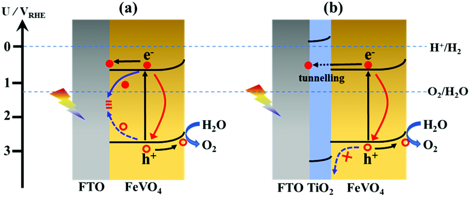 | ||
| Fig. 1 Schematic band alignment of charge transport and recombination models in (a) FeVO4/FTO and (b) FeVO4/TiO2/FTO photoanodes. | ||
Recently, the introduction of an interfacial layer between a transparent conducting substrate and photoanode has been demonstrated as a promising approach to address the issue of charge recombination at the transparent conducting substrate|photoanode interface.23–26 Toward this end, TiO2 was employed as the interfacial layer between FTO and FeVO4 in this study, owing to its unique electronic features (Fig. S1†). In Fig. 1b, the TiO2 interfacial layer can be seen to be functionalized as an effective hole blocking barrier to suppress back hole transfer from FeVO4 to FTO, as a result of a large valence band offset between TiO2 and FeVO4. This is rather beneficial to reduce the charge recombination at the FeVO4|FTO interface, and thus significantly improves the charge collection efficiency. However, the fabrication of a TiO2 blocking layer is very challenging, because its relatively higher conduction band position over FeVO4 is unfavorable for electron transfer and collection. To make sure that the photogenerated electrons can freely tunnel from the FeVO4 photoanode to the FTO collector, an ultrathin and conformal TiO2 interfacial layer is highly essential. If its thickness is beyond the electron tunnelling distance, the TiO2 interfacial layer would bring about a negative effect and alleviate the PEC water splitting performance. Herein, to better achieve the atomic-scale control of the TiO2 thickness as well as its conformal covering on the FTO substrate, an atomic layer deposition (ALD) method was employed for the fabrication of the TiO2 interfacial layer. Incident photocurrent conversion efficiency (IPCE), electrochemical impedance spectroscopy (EIS) and Mott–Schottky (M–S) measurements were carried out to study the promotional effect of the TiO2 interfacial layer. These results indicated that a 1.1 nm TiO2 interfacial layer can efficiently block the back transfer hole and suppress the charge recombination at the FTO|FeVO4 interface, leading to the enhancement in the PEC water splitting performance over the FeVO4 photoanode. We believe that the strategy of fabricating an ultrathin TiO2 interfacial layer as a hole blocking barrier can also benefit other photoanodes.
Experimental section
Materials
Iron(III) nitrate nonahydrate (Fe(NO3)3·9H2O), ammonium metavanadate (NH4VO3), nitric acid (HNO3, 68%), and ethylene glycol were purchased from Sinopharm Chemical Reagent Co. Ltd. (China). Succinic acid was provided by Aladdin Industrial Corporation. The ALD source of titanium(IV) isopropoxide was provided by J&K Scientific Ltd. All chemical reagents were of analytical grade and used without further purification.Electrode preparation
Conductive fluorine-doped tin oxide (FTO)-coated glass (1 cm × 4 cm) was cleaned using acetone, ethanol, isopropanol and deionized water respectively. It was then transferred into an ALD chamber heated to 150 °C with the conductive side facing up. Titanium(IV) isopropoxide and deionized water were used as sources of ALD and kept in customized containers. The titanium source was heated to 80 °C. Each cycle was completed in 0.8 s and 0.1 s pulse time for the titanium source and water source. The purge durations of the titanium and water sources were 20 s and 25 s respectively. The TiO2 underlayers with different thicknesses were obtained by depositing with different cycles.The fabrication of the FeVO4 film was modified according to a previously reported sol–gel procedure.20 Typically, 0.5 mmol Fe(NO3)3·9H2O, 0.5 mmol NH4VO3 and 0.5 mmol succinic acid were dissolved in 9.6 mL ethylene glycol and 0.4 mL HNO3 under sonication. 20 μL precursor solution was dropped on bare FTO or as-prepared TiO2 modified FTO with an area of 1 cm × 2 cm and subsequently dried on a hot plate at 70 °C for 20 min. The films then were annealed in a furnace in air at 500 °C for 1 h.
Characterization and analysis
X-ray diffraction (XRD) patterns were obtained on a Bruker D8 Advance X-ray diffractometer (Cu K1 irradiation, λ = 1.5406 Å). The morphology of samples and corresponding EDX data were obtained by using a field-emission scanning electron microscope (SEM, Helios G4 CX). A detailed microscopic structure was observed by using a high-resolution scanning transmission electron microscope (HRTEM, FEI TECNAI G2 F20). X-ray photoelectron spectroscopy (XPS) measurement was performed on an X-ray photoelectron spectrometer (XPS, Thermo Scientific ESCA Lab250), with monochromatic Al Kα as the X-ray source. The ultraviolet-visible light absorbance spectrum was measured using a Thermo Scientific GENEYSY 10S UV-vis spectrometer. Raman spectrum measurement was performed with a multichannel modular triple Raman system (LabRAM HR Evolution) using a confocal microscope with a 532 nm excitation laser. The electrochemical measurement was carried out using a potentiostat (Bio-Logic SP-150). Mott–Schottky (M–S) spectra were obtained in the potential range of 0.4–1.6 VRHE at a frequency of 1 kHz in the dark. Electrochemical impedance spectrum (EIS) measurement was carried out with an amplitude of 10 mV at a potential of 1.6 VRHE with simulated solar illumination over a frequency range from 0.1–100![[thin space (1/6-em)]](https://www.rsc.org/images/entities/char_2009.gif) 000 Hz.
000 Hz.
PEC performance measurements
The PEC performance measurements of the photoanodes were carried out by using a CHI 660E electrochemical workstation using a typical three-electrode configuration, with the FeVO4 photoanode as the working electrode, platinum foil as the counter electrode, and Ag/AgCl (3 M KCl) as the reference electrode. The potential of the electrode was converted into the reversible hydrogen electrode (RHE) potential according to the formula ERHE = EAg/AgCl + 0.059 pH + EAg/AgClθ (0.1976 V). PEC performance and IPCE measurements were achieved in 0.1 M potassium phosphate buffer solution (pH 7.0) with back-side illumination, and the irradiance intensity was about 70 mW cm−2 measured by using a spectroradiometer. IPCE was measured under a xenon lamp equipped with band pass filters to provide approximate monochromatic light.Results and discussion
In Fig. 2a and b, the SEM images were collected to study the morphology of the FTO substrate before and after ALD modification. There was no obvious change observed on the surface of FTO after being deposited with a 15-cycle TiO2 layer. This could be because a 15-cycle TiO2 layer is too thin to be discerned. To better determine the thickness of the TiO2 interfacial layer, a control experiment of depositing a 300-cycle TiO2 layer was conducted to calculate the growth rate of TiO2 on the FTO substrate. According to the cross-sectional SEM image in Fig. S2,† the thickness of a 300-cycle TiO2 layer was determined to be 22 nm, indicating that the growth rate of TiO2 was around 0.07 nm per deposition cycle. Based on this calculation, the thickness of a 15-cycle TiO2 layer was determined to be 1.1 nm. This is an ultrathin interfacial layer that can allow free tunnelling for photogenerated electrons from FeVO4 to FTO. To better identify this ultrathin TiO2 layer on the FTO substrate, the XPS spectrum was obtained. As shown in Fig. 2c, two evident peaks at 458.7 and 463.8 eV were observed in the Ti 2p spectrum for ALD modified FTO. These binding energies correspond to Ti 2p3/2 and Ti 2p1/2, respectively,27 suggesting the existence of TiO2 on the FTO substrate. To further demonstrate the presence of the TiO2 interfacial layer on FTO and study its influence on the surface properties of the FTO substrate, the contact angles were examined. In Fig. 2d, the contact angles of bare FTO are determined to be 87.0° in the dark and 85.9° after being irradiated by using a UV lamp for 20 min, respectively, indicative of the hydrophobic nature of the FTO surface. After being modified with a 1.1 nm-thick TiO2 interfacial layer, the contact angles decrease to 40.3° in the dark and 32.1° after UV lamp irradiation, respectively. This finding indicates that the TiO2 interfacial layer can significantly improve the surface hydrophilicity of FTO, even when its thickness is as small as 1.1 nm. This improved hydrophilic surface could be advantageous to construct an FeVO4 overlayer on it with good adherence. | ||
| Fig. 2 (a and b) SEM images of the samples, (c) XPS spectra and (d) surface contact angle of a water droplet on the surface of FTO and TiO2/FTO. | ||
The TiO2 modified FTO substrate (TiO2/FTO) was then used for the fabrication of the FeVO4 photoanode. Fig. 3a shows the XRD patterns of the FeVO4/TiO2/FTO photoanode, together with FeVO4/FTO as the control sample. Along with the feature of SnO2 from the FTO substrate, some weak diffraction peaks can be assigned to the characteristics of triclinic phase FeVO4 (JCPDS no. 38-1372), which is also present in the XRD patterns. The poor crystallinity could be caused by insufficient high annealing temperature; this can be confirmed from the higher crystallinity of FeVO4 obtained at higher temperature (Fig. S3†). As shown in Fig. S4a,† the powder scraped from the FeVO4/TiO2/FTO photoanode was subjected to TEM analysis. The interplanar spacing of 0.32 nm and 0.38 nm can be identified as (−220) and (200) planes of FeVO4, respectively.20 The electron diffraction pattern displays multiple-ring diffraction (Fig. S4b†). These observations illustrate the polycrystalline feature of FeVO4 particles.
 | ||
| Fig. 3 (a) XRD patterns and (b) Raman spectra of the samples. | ||
As shown in Fig. 3b, the crystalline structure of the FeVO4/TiO2/FTO photoanode was further characterized using the Raman spectrum. Similar to the results of XRD patterns, both FeVO4/TiO2/FTO and FeVO4/FTO photoanodes exhibit the characteristic modes of triclinic FeVO4. For example, the broad peak at ∼308 cm−1 can be assigned to the stretching vibration in non-equivalent Fe–O bonds.28 The peaks at 355 and 445 cm−1 can be attributed to V–O–V deformation. The peak of 640 cm−1 possibly arises from Fe–O stretching vibrations in FeO5 distorted trigonal bipyramids.17 The peaks at 884, 912 and 944 cm−1 correspond to the stretching vibrations of the terminal V![[double bond, length as m-dash]](https://www.rsc.org/images/entities/char_e001.gif) O bonds in the VO4 polyhedron.29 No peaks found in the range of 1000–1026 cm−1 rule out the extra V2O5 impurity phase.30 Clearly, no evident difference in Raman spectra can be found between FeVO4/TiO2/FTO and FeVO4/FTO photoanodes, indicating that the introduction of the TiO2 interfacial layer on the FTO substrate could not influence the crystalline structure of the FeVO4 film.
O bonds in the VO4 polyhedron.29 No peaks found in the range of 1000–1026 cm−1 rule out the extra V2O5 impurity phase.30 Clearly, no evident difference in Raman spectra can be found between FeVO4/TiO2/FTO and FeVO4/FTO photoanodes, indicating that the introduction of the TiO2 interfacial layer on the FTO substrate could not influence the crystalline structure of the FeVO4 film.
As shown in Fig. 4a and b, the FeVO4/FTO and FeVO4/TiO2/FTO photoanodes were imaged by SEM. It can be observed that both electrodes have a similar morphology, with 260–270 nm thickness of porous FeVO4. The porous structure is caused by the removal of organic compounds after the calcination of the metal–organic unit involved in the electrode preparation. This could increase the interfacial area between the photoelectrode and electrolyte, which is favourable for the water oxidation reaction. The electric double layer capacitance is often employed to assess the electrochemical surface area (ECSA) of an electrode.31,32 The CV curves for the electrodes were recorded at different scan rates in the region of 1.2–1.4 VRHE (Fig. S5†), and the differences between the anodic and cathodic current densities {ΔJ = (Ja − Jc)} at a potential of 1.3 VRHE were plotted against the scan rate to obtain the measured capacitance (Fig. 4c). FeVO4/TiO2/FTO (168 μF cm−2) has a comparable electrochemically active surface area to FeVO4/FTO (173 μF cm−2). As shown in Fig. 4d, UV-vis absorption spectroscopy was carried out to investigate the optical properties of the electrodes. The electrodes exhibit an absorption onset of about 590 nm, in agreement with a reported value.18 Compared to those of FeVO4/FTO, no evident change in optical properties happens to FeVO4/TiO2/FTO, indicating that the ultrathin TiO2 interfacial layer cannot obviously affect the light harvesting ability of the FeVO4 photoanode.
 | ||
| Fig. 4 (a and b) SEM images, (c) the differences in current density variation plotted against the scan rate curves, (d) UV-vis absorption spectra, (e) Mott–Schottky plots and (f) Nyquist plots of the samples. | ||
To study the effect of the thin TiO2 underlayer on the semiconductor band structure and conductivity in the FeVO4 photoelectrode, M–S analysis for the electrodes was carried out in the dark. On the basis of the M–S plots, the carrier density (ND) and flat band potential (Efb) for the photoelectrodes can be calculated using the M–S equation.32 It is noted that the M–S equation is derived from the plate electrode, and thus the deduced carrier density is only used for comparison in this study.33 In Fig. 4e, the M–S curves have positive slopes, indicative of n-type conductivity. The comparable linear slope of FeVO4/FTO and FeVO4/TiO2/FTO means their similar ND value; this can rule out the diffusion of Ti from the interfacial TiO2 layer into the FeVO4 film during the electrode preparation. Additionally, the flat-band potential for the electrodes is determined to be 0.7 VRHE, which is in good agreement with a reported value.25 In Fig. 4f, Nyquist plots recorded under illumination were obtained to study the charge transfer behaviour of the photoanodes. The obtained Nyquist plots (Fig. 4f) can be fitted with an equivalent circuit diagram (the inset in Fig. 4f),34,35 which consists of three parts of resistances: the series resistance in the PEC cell (Rs), the charge transport resistance in the bulk related to the charge trapping (RB) and the charge transfer resistance at the electrode–electrolyte interface associated with the hole transfer process (RI). In Table S1,† FeVO4/TiO2/FTO has much lower RB and RI than FeVO4/FTO, indicating that the thin TiO2 layer acts an efficient blocking layer on the FTO to reduce the recombination of photoinduced electron–hole pairs in the bulk while enhancing the charge transfer in the photoanode. The photogenerated carrier recombination properties of the electrodes were also investigated using the photoluminescence spectrum. In Fig. S6,† FeVO4/TiO2/FTO has a much lower photoluminescence intensity in comparison to FeVO4/FTO; this further confirms that the introduction of the ultrathin TiO2 layer significantly inhibits the recombination of the photogenerated electron/hole pairs. This will lead to an enhanced PEC performance of the FeVO4 photoanode.
To investigate the effect of the TiO2 underlayer on the PEC performance of FeVO4 electrodes, linear sweep voltammetry (LSV) curves were obtained under dark conditions or simulated solar light irradiation. In Fig. 5a, TiO2/FTO shows a negligible photocurrent due to the ultrathin TiO2 film on FTO; this rules out the contribution of TiO2 to the PEC performance of FeVO4/FTO. Both FeVO4/FTO and FeVO4/TiO2/FTO display a similar onset potential of 1.1 VRHE. Interestingly, the introduction of the TiO2 underlayer obviously enhances the photocurrent of the FeVO4 photoanode, and FeVO4/TiO2/FTO displays a photocurrent density of 0.35 mA cm−2 at 1.6 VRHE, which is about 35% higher than that of FeVO4/FTO (0.26 mA cm−2). We also calculated the ECSA-normalized photocurrent for the electrodes; the value at 1.6 VRHE is 2.1 A F−1 for FeVO4/TiO2/FTO, which is about 40% higher than that of FeVO4/FTO (1.5 A F−1). This also confirms the promotion effect of the TiO2 interfacial layer. The PEC performance of FeVO4/TiO2/FTO with different TiO2 deposition cycles was also studied (Fig. S7†), and the result indicates that the photocurrent density increases initially, and then reaches a maximum when the deposition cycle number is 15. A further increase in the thickness of TiO2 results in a decrease in the photocurrent density. The reason is that a thicker TiO2 interfacial layer is not favourable for free electron tunnelling. This can be confirmed from the higher RB value of FeVO4/TiO2/FTO when the TiO2 deposition cycle number increases to 100 (Fig. S8 and Table S1†).
 | ||
| Fig. 5 (a) The photocurrent density–potential curves for the PEC water oxidation reaction, (b) IPCE spectra measured at a potential of 1.6 VRHE, (c) the charge-injection efficiency (ηinj) and the charge-separation efficiency (ηsep) versus applied potential curves, and (d) photocurrent density–time curves for the electrodes. | ||
To further investigate the relationship between PEC performance and optical absorption properties of the photoanodes, the incident-photon-to-current-efficiency (IPCE) test was carried out to evaluate the spectral response in the range of 340–630 nm at 1.6 VRHE. As displayed in Fig. 5b, the profile for the IPCE curve mostly follows the trend of the UV-vis optical absorption spectrum shown in Fig. 4d. This indicates that the PEC performance is closely related to the light absorption due to band–band transition in the FeVO4 film. In comparison to FeVO4/FTO, FeVO4/TiO2/FTO shows a higher IPCE value. Additionally, we also investigated the charge-separation and charge-injection efficiency differences between TiO2/FTO and FeVO4/FTO photoanodes (Fig. S9†). As shown in Fig. 5c, the introduction of the TiO2 interfacial layer obviously increases the charge separation efficiency for water oxidation over the FeVO4 electrode, while it has negligible effect on the charge-injection efficiency. Photocurrent stability is very important for future practical application of photoelectrode materials. In Fig. 5d, the decrease in the photocurrent is observed for the electrodes in the stability test of 2 h, with the losses of 21% and 23% over FeVO4/FTO and FeVO4/TiO2/FTO, respectively. This could be due to the intrinsic photocorrosion related to the loss of vanadium ions from metal vanadate photoanodes.36,37 Of course, the improvement in the stability is needed in the next step. Furthermore, the TiO2 underlayer can also promote the PEC performance of the BiVO4 photoanode grown on the FTO substrate (Fig. S10†), as a result of suppressing recombination of electron–hole pairs at the interface. This indicates that the advantage of the thin TiO2 underlayer could be extended to improve other photoanodes grown on a conducting substrate.
Conclusions
In summary, we have demonstrated that the introduction of an ultrathin TiO2 layer between the FTO substrate and FeVO4 photoanode by ALD technology is a promising strategy to address the issue of interfacial charge recombination. As a result of its unique electronic features, in particular its band structure, the ultrathin TiO2 interfacial layer can function as an effective hole blocking barrier to suppress back hole transfer from FeVO4 to FTO, and thus reduces the charge recombination at the FTO/FeVO4 interface. Compared with the sample synthesized by directly growing FeVO4 on FTO, FeVO4/TiO2/FTO exhibited enhanced PEC water splitting performance. Furthermore, we believe that the strategy of fabricating an ultrathin TiO2 interfacial layer as a hole blocking barrier can also benefit other photoanodes.Conflicts of interest
There are no conflicts to declare.Acknowledgements
The work was supported by NSFC (U1805255, 21972022, and 22072021), Natural Science Foundation of Fujian Province (2018J01681), the Award Program for Outstanding Young Innovative Talents of Fujian province (00332111), and the Independent Research Project of State Key Laboratory of Photocatalysis on Energy and Environment (SKLPEE-2017A03).Notes and references
- A. Fujishima and K. Honda, Nature, 1972, 238, 37–38 CrossRef CAS.
- Z. S. Li, W. J. Luo, M. L. Zhang, J. Y. Feng and Z. G. Zou, Energy Environ. Sci., 2013, 6, 347–370 RSC.
- M. G. Walter, E. L. Warren, J. R. McKone, S. W. Boettcher, Q. X. Mi, E. A. Santori and N. S. Lewis, Chem. Rev., 2010, 110, 6446–6473 CrossRef CAS.
- K. Sivula, F. Le Formal and M. Gratzel, Chemsuschem, 2011, 4, 432–449 CrossRef CAS.
- J. W. Huang, P. F. Yue, L. Wang, H. D. She and Q. Z. Wang, Chin. J. Catal., 2019, 40, 1408–1420 CrossRef CAS.
- Y. Park, K. J. McDonald and K. S. Choi, Chem. Soc. Rev., 2013, 42, 2321–2337 RSC.
- C. R. Liang, J. L. Xie, J. Y. Xiong, L. P. Gong and C. M. Li, Sustainable Energy Fuels, 2018, 2, 2053–2509 RSC.
- T. Higashi, H. Nishiyama, Y. Suzuki, Y. Sasaki, T. Hisatomi, M. Katayama, T. Minegishi, K. Seki, T. Yamada and K. Domen, Angew. Chem., Int. Ed., 2019, 58, 2300–2304 CrossRef CAS.
- E. S. Kim, N. Nishimura, G. Magesh, J. Y. Kim, J. W. Jang, H. Jun, J. Kubota, K. Domen and J. S. Lee, J. Am. Chem. Soc., 2013, 135, 5375–5383 CrossRef CAS.
- W. Xiong, F. Huang and R. Q. Zhang, Sustainable Energy Fuels, 2020, 4, 485–503 RSC.
- J. H. Yang, D. G. Wang, H. X. Han and C. Li, Acc. Chem. Res., 2013, 46, 1900–1909 CrossRef.
- R. Liu, Z. Zheng, J. Spurgeon and X. G. Yang, Energy Environ. Sci., 2014, 7, 2504–2517 RSC.
- C. R. Jiang, S. J. A. Moniz, A. Q. Wang, T. Zhang and J. W. Tang, Chem. Soc. Rev., 2017, 46, 4645–4660 RSC.
- T. Arai, Y. Konishi, Y. Iwasaki, H. Sugihara and K. Sayama, J. Comb. Chem., 2007, 9, 574–581 CrossRef.
- C. D. Morton, I. J. Slipper, M. J. K. Thomas and B. D. Alexander, J. Photochem. Photobiol., A, 2010, 216, 209–214 CrossRef.
- S. K. Biswas and J. O. Baeg, Int. J. Hydrogen Energy, 2013, 38, 14451–14457 CrossRef.
- H. Mandal, S. Shyamal, P. Hajra, A. Bera, D. Sariket, S. Kundu and C. Bhattacharya, RSC Adv., 2016, 6, 4992–4999 RSC.
- W. Wang, Y. J. Zhang, L. Wang and Y. P. Bi, J. Mater. Chem. A, 2017, 5, 2478–2482 RSC.
- M. Y. Zhang, Y. M. Ma, D. Friedrich, R. van de Krol, L. H. Wong and F. F. Abdi, J. Mater. Chem. A, 2018, 6, 548–555 RSC.
- J. Y. Feng, Z. Q. Wang, X. Zhao, G. Yang, B. W. Zhang, Z. Chen and Y. Z. Huang, J. Phys. Chem. C, 2018, 122, 9773–9782 CrossRef CAS.
- J. Quinonero and R. Gomez, Appl. Catal., B, 2017, 217, 437–447 CrossRef CAS.
- B. Lamm, L. T. Zhou, P. Rao and M. Stefik, Chemsuschem, 2019, 12, 1916–1924 CrossRef CAS.
- T. Hisatomi, H. Dotan, M. Stefik, K. Sivula, A. Rothschild, M. Gratzel and N. Mathews, Adv. Mater., 2012, 24, 2699–2702 CrossRef CAS.
- A. Annamalai, P. S. Shinde, A. Subramanian, J. Y. Kim, J. H. Kim, S. H. Choi, J. S. Lee and J. S. Jang, J. Mater. Chem. A, 2015, 3, 5007–5013 RSC.
- D. G. Wang, G. L. Chang, Y. Y. Zhang, J. Chao, J. Z. Yang, S. Su, L. H. Wang, C. H. Fan and L. H. Wang, Nanoscale, 2016, 8, 12697–12701 RSC.
- Z. W. Fan, Z. Xu, S. C. Yan and Z. G. Zou, J. Mater. Chem. A, 2017, 5, 8402–8407 RSC.
- C. Zheng, Z. Z. Zhu, S. B. Wang and Y. D. Hou, Appl. Surf. Sci., 2015, 359, 805–811 CrossRef CAS.
- D. P. Dutta, M. Ramakrishnan, M. Roy and A. Kumar, J. Photochem. Photobiol., A, 2017, 335, 102–111 CrossRef CAS.
- Z. D. Liu, Q. F. Lu, M. Z. Wei and E. Y. Guo, J. Sol-Gel Sci. Technol., 2017, 82, 67–74 CrossRef CAS.
- N. L. Wang, J. E. Qiu, J. Wu, K. Y. You and H. A. Luo, Catal. Lett., 2015, 145, 1792–1797 CrossRef CAS.
- M. W. Louie and A. T. Bell, J. Am. Chem. Soc., 2013, 135, 12329–12337 CrossRef CAS.
- Y. D. Hou, C. Zheng, Z. Z. Zhu and X. C. Wang, Chem. Commun., 2016, 52, 6888–6891 RSC.
- K. Zhang, T. J. Dong, G. C. Xie, L. M. Guan, B. D. Guo, Q. Xiang, Y. W. Dai, L. Q. Tian, A. Batool, S. U. Jan, R. Boddula, A. A. Thebo and J. R. Gong, ACS Appl. Mater. Interfaces, 2017, 9, 42723–42733 CrossRef CAS.
- C. C. Li, A. Li, Z. B. Luo, J. J. Zhang, X. X. Chang, Z. Q. Huang, T. Wang and J. L. Gong, Angew. Chem., Int. Ed., 2017, 56, 4150–4155 CrossRef CAS.
- T. L. Kim, M. J. Choi, T. H. Lee, W. Sohn and H. W. Jang, Nano Lett., 2019, 19, 5897–5903 CrossRef CAS.
- D. K. Lee and K. S. Choi, Nat. Energy, 2018, 3, 53–60 CrossRef CAS.
- L. Zhou, A. Shinde, D. Guevarra, F. M. Toma, H. S. Stein, J. M. Gregoire and J. A. Haber, ACS Appl. Energy Mater., 2018, 1, 5766–5771 CAS.
Footnote |
| † Electronic supplementary information (ESI) available. See DOI: 10.1039/d0se01546f |
| This journal is © The Royal Society of Chemistry 2021 |