
Unravelling the theoretical window to fabricate high performance inorganic perovskite solar cells
Yassine
Raoui
ac,
Hamid
Ez-Zahraouy
c,
Shahzada
Ahmad
 *ab and
Samrana
Kazim
*ab
*ab and
Samrana
Kazim
*ab
aBCMaterials, Basque Center for Materials, Applications and Nanostructures, Bld. Martina Casiano, UPV/EHU Science Park, Barrio Sarriena s/n, 48940 Leioa, Spain. E-mail: samrana.kazim@bcmaterials.net; shahzada.ahmad@bcmaterials.net
bIKERBASQUE, Basque Foundation for Science, Bilbao 48013, Spain
cLaboratory of Condensed Matter and Interdisciplinary Sciences, Faculty of Sciences, Mohammed V University in Rabat, Morocco
First published on 4th November 2020
Abstract
Perovskite solar cells (PSCs) have experienced a decade of intense investigation as a promising photovoltaic technology, having a power conversion efficiency of 25.5% with the use of lead based light harvesters. Recently, inorganic cesium cation based mixed halide perovskites (CsMI3−xBrx, M = Pb or Sn) as absorbers in PSCs gave promising results; in particular CsPbI2Br demonstrated improved thermal stability and carrier transport properties. However, the performance is far-off from the theoretical limit due to intriguing issues such as high defect density (Nt) and energy level mismatch. Such barriers can be overcome through device modelling and unraveling the kinetics. Here we have employed a computational approach to design and investigate CsPbI2Br based solar cells by elucidating the role of defect density in the performance and further different types of hole transport layers via optimizing their valence band offset and the barrier height at the back contact was also probed. By optimizing such parameters for CsPbI2Br, power conversion efficiencies of 17.71, 17.44 and 17.54% using CuSCN, PTAA and spiro-OMeTAD as hole selective layers respectively can be reached. Furthermore, lead free CsSnI3−xBrx (0 < x < 3) based PSCs were simulated and the effect of band gap variation as a result of the Br content was studied on the performance. The influence of the defect density of the absorber layer (CsSnIBr2) at interfaces was studied, and with optimized defect density CsSnIBr2 based PSCs gave an efficiency of 20.32% with a Voc of 1.35 V when SnO2 was used as the electron transport layer and spiro-OMeTAD as the HTM. Our approach suggests ways for experimental design protocols to achieve high performance inorganic Pb and Sn based PSCs.
1. Introduction
Solar energy is one of the most promising sources of energy to counter the adverse effect of climate change on our planet. Emerging photovoltaic technologies can potentially reach the masses, particularly perovskite solar cells (PSCs). Hybrid organic–inorganic lead (Pb) based perovskites as light absorbers are the most investigated due to their excellent electro-optical properties1–5 and gave record performance.6,7 However, hybrid organic–inorganic lead halide perovskites suffer from challenges such as inadequate efficiency8 and thermal instability at high temperature, originating due to the volatile nature of organic cations (FA and MA).9,10 Replacement of organic cations with inorganic cations such as Cs is found to be an effective approach to overcome such bottlenecks.11,12 However, CsPbI3 was noted to be stable only in the form of a cubic perovskite (α-phase) at high temperature, which can be easily converted to an orthorhombic non-perovskite (δ) phase.13 In this context, CsPbI3−xBrx evolved as a promising absorber for PSCs in terms of phase stability. CsPbI2Br stability in the cubic phase at room temperature with a band gap of 1.82–1.92 eV was reported.14 Partial substitution of I with Br in CsPbI3 stabilizes the cubic phase, led to intense investigation and a performance of CsPbI2Br based PSCs up to 16.07% was reported.15 Such results were obtained by reducing the defect density in the active layer, growth control of CsPbI2Br through optimized annealing temperature,16 using an effective anti-solvent approach17 or minimizing the energy level gap at charge selective layers,18 similar to that in hybrid lead halide PSCs.19 However, the performance remains lower than the 22.1% theoretical limit of PCE with 1.65 Voc, when 500 nm thick CsPbI2Br was used.20 To achieve the theoretical efficiency limit, the strategy should be to focus on reducing the defect density of the active layer, which should be less than 3.64 × 1015 cm−3.21 The energetic alignment at charge selective layers needs further optimization using p-type conducting polymers or inorganic semiconductors to minimize energy loss (Eloss = Eg − eVoc, Eg is the band gap and e is the elementary charge). Arguably, efficient CsPbI2Br based PSCs should focus on reducing Eloss as much as possible by improving Voc and Jsc, and this target can be achieved through band alignment and high quality CsPbI2Br crystal formation. The efficient CsPbI2Br based PSCs yielded a PCE of 16.79% with a Voc of 1.32 V, i.e. Eloss = 0.59 eV.22The toxicity of the lead (Pb) metal is visualized as a barrier for potential commercial success of inorganic PSCs. The use of tin (Sn) as a possible metal to replace the problematic Pb is being investigated.23 Compared to Pb-based perovskites, Sn-based perovskites showed high optical absorption coefficients,24,25 narrow optical band gaps and high charge carrier mobilities.26 In accordance with the perovskite structure (ABX3), the A cation can be MA, FA and Cs, and in the case of the MA cation an efficiency of 6.4% was achieved by using MASnI3 as the light harvester having a band gap of 1.3 eV.27 Further, using the FA cation (a slightly larger cation than MA), Koh et al. prepared FASnI3 with the incorporation of 20% SnF2, and a PCE of 2.10% was reported with a band gap of 1.41 eV.28 However, the instability of organic–inorganic halide perovskites is of concern, due to the use of organic cations under outdoor conditions.29 To resolve this stability issue, Cs as an A cation was opted for all inorganic Sn-based perovskites with X = I and Br, which have similar electro-optical properties to FASnI3 and MASnI3. The first report using Sn-based perovskites was with CsSnI3 that acted as a hole transport layer (HTL) and yielded a PCE of 0.9%.30 However, the instability of Sn in the +2 oxidation state, allowing easy conversion to the +4 state in the presence of moisture and oxygen,31 was a limiting factor. To resolve the oxidation issues of Sn, SnCl2 and SnF2 as reducing agents were exploited to minimize the extent of p-type self-doping of perovskites and to reduce the hole carrier density, in order to improve the performance.32,33 Besides, a mixed anion containing CsSnI3−xBrx as the light harvester has been studied, and its band gap was tuned from 1.27–1.74 eV by varying the percentage of Br from x = 0–1.34
Although these inorganic Sn-based PSCs show lower performance compared to their Pb based counterparts, their low band gap exhibits high potential for perovskite–perovskite tandem solar cells. Further, investigation of a macroscopic device model of inorganic Sn-based PSCs is still obscure and issues need to be resolved to improve Sn-based PSCs, such as prevention of bulk and interface recombination due to tin vacancies, and rational designing of charge selective contacts to efficiently extract carriers from perovskites. The issue of high hole carrier density as a result of self p-doping can be controlled by SnF2 addition, which will allow reduction of the defect density from a pristine value of 1.1 × 1019 cm−3 to 5.7 × 1017 cm−3 for CsSnI3. It can be further reduced by substitution of I with Br. Taking this into account, we performed theoretical investigation for CsPbI2Br and CsSnI3−xBrx based PSCs. Firstly, we focus on CsPbI2Br by studying the effect of interface engineering at the HTL and perovskite interface by employing different HTLs such as organic (spiro-OMeTAD), inorganic (CuSCN) and polymeric (PTAA) materials. Additionally, the influence of the defect density of the CsPbI2Br absorber layer on performance was studied. The HTL is a channel to transfer the holes from the active layer to the back contact that needs to be optimized for alignment. Most of the studies on PSCs are focused on optimizing the valence and conduction band offset, which is critical for transport and extraction of charges as the height of the energy barrier regulates the contact resistance. However, reports showing the effect of energy band alignment between a HTM and back contact are scarce. We reported how the valence band offset (VBO) can be optimized to boost the performance of PSCs.35 Thus to address the mismatch alignment at the perovskite/HTM/back contact, firstly, we elucidated the impact of the valence band maximum (VBM) of HTMs (spiro-OMeTAD, CuSCN & PTAA) on the performance of CsPbI2Br based PSCs and also on the interface between the HTM and back contact. During this process, we discovered that modulating the Ev (i.e. varying the electron affinity) of the HTM leads to formation of arc shape at the HTM/back contact, its curvature changes with the variation of Ev and has strong influence on the performance of PSCs. Such optimizations led to an efficiency of 17.73, 17.45 and 17.44% using CuSCN, PTAA and spiro-OMeTAD as HTMs respectively.
Secondly, we ran simulation for lead free Sn-based inorganic PSCs, where the effect of I anion substitution with Br in the CsSnI3 absorber was investigated to clarify its impact on the conduction band offset (CBO), i.e., the difference between the conduction band minimum (CBM) energy levels of the ETL and those of the perovskite layer, ΔEc = Ec_ETL − Ec_absorber.
To our knowledge, there are no theoretical or experimental studies on lead free inorganic PSCs are reported in detailed. The “self-doping” in Sn-based inorganic PSCs allows lowering the trap density and its impact on the solar cell performance was studied. We studied the influence of defect density variation in the absorber layer and at its interfaces to elucidate the optimum values that can boost the efficiency, we computed a 20.35% PCE with a Voc of 1.35 V.
2. Theory and computational details
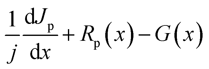
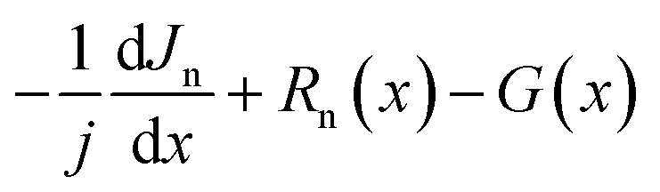
The simulations were performed using SCAPS 3.3.07 software,19 based on the Poisson equation (1), and continuity equations for electrons (2) and holes (3):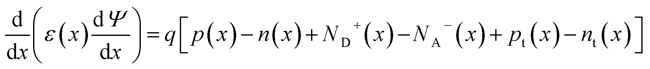 | (1) |
 | (2) |
 | (3) |
The symbols presented in Tables 1 and 4 can be described as follows: NA and ND denote acceptor and donor densities, εr is relative permittivity, χ is electron affinity, Eg is the band gap energy, Nt is defect density, and μn and μp are the mobility of electrons and holes respectively. Computational studies were performed on a planar PSC with an architecture of FTO/SnO2/interfacial layer 1 (IL1)/inorganic perovskite/interfacial layer 2 (IL2)/HTM/Au. The defect type in the bulk perovskite is considered neutral with a cross section of electrons and holes of 2 × 10⁻¹⁴ cm2. The electron and hole thermal velocity was 107 cm s−1. Gold (Au) was used as the back contact while fluorine doped tin oxide (FTO) as the front contact.
| Parameter | IL1 | CsPbI2Br | IL2 | PTAA | CuSCN19 |
|---|---|---|---|---|---|
| Thickness (nm) | 10 | 500 | 10 | 150 | 150 |
| E g (eV) | 1.86 (ref. 37) | 1.86 (ref. 37) | 1.86 (ref. 37) | 2.95 (ref. 38) | 3.6 |
| χ | 3.8 (ref. 37) | 3.8 (ref. 37) | 3.8 (ref. 37) | 2.3 (ref. 38) | 1.7 |
| ε r | 8.6 | 8.6 | 8.6 | 3.5 (ref. 39) | 10 |
| N c (1/cm3) | 2.2 × 10¹⁸ | 2.2 × 10¹⁸ | 2.2 × 10¹⁸ | 2.2 × 10¹⁸ | 2.5 × 10¹⁸ |
| N v (1/cm3) | 1.8 × 10¹⁹ | 1.8 × 10¹⁹ | 1.8 × 10¹⁹ | 1.8 × 10¹⁹ | 1.8 × 10¹⁹ |
| μ n (cm2 V−1 s−1) | 200 (ref. 40) | 200 (ref. 40) | 200 (ref. 40) | 1 × 10⁻⁴ (ref. 41) | 100 |
| μ p (cm2 V−1 s−1) | 200 | 200 | 200 | 1 × 10⁻⁴ | 25 |
| N A (1/cm3) | — | — | — | — | 1 × 10¹⁸ |
| N D (1/cm3) | 1 × 10¹⁵ | 1 × 10¹⁵ | 1 × 10¹⁵ | 1 × 10¹⁸ | — |
| N t (1/cm3) | 3.64 × 10¹⁶ | 3.64 × 10¹⁵ (ref. 21) | 3.64 × 10¹⁶ | 1 × 10¹⁵ | 1 × 10¹⁵ |
Before detailing the band alignment at the HTM–back contact, it is imperative to understand the condition for the formation of the junction between the p-type semiconductor (HTM) and metal for the flow of holes.36
Fig. 1 shows the energy band diagrams for semiconductor–metal interfaces, where ϕ is the work function and sp and m refer to the p-type semiconductor and metal respectively. EF is the Fermi-energy and χ is the electron affinity. If the metal and semiconductor are brought together, two types of contacts can be formed depending on the difference of the work function of the metal and semiconductor: Schottky and ohmic junctions (Fig. 1a and b). The type of interface is a result of the levelling of work functions to balance the chemical potential. When the work function of the p-type semiconducting HTM (ϕsp) is higher than that of the metal (Fig. 1a), an energy barrier is formed for holes and a Schottky contact is created. In contrast, if the work function of the HTM (ϕsp) is lower than that of the metal (ϕm), an ohmic contact will be formed (Fig. 1b). To analyze the effect of these two interfacial contacts on the performance of PSCs, we will vary the valence energy level (Ev_HTM) of spiro-OMeTAD and PTAA as HTMs (by changing the electron affinity) with respect to the valence energy level of the absorber (Ev_absorber), and interfaces at the HTM/metal. The optimized VBO of each HTM will be the point where the performance of CsPbI2Br PSCs is maximized. The VBO is the difference between the valence band energy of the perovskite layer and those of HTMs, ΔEv = Ev_absorber − Ev_HTM.
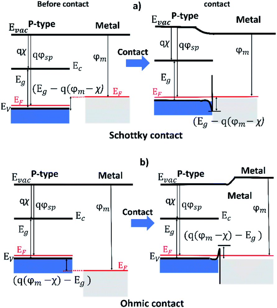 | ||
| Fig. 1 Energy band diagrams for semiconductor–metal interfaces for (a) Schottky contact and (b) ohmic contact. | ||
The barrier height between a p-type semiconductor and metal can be given by {(ϕBp = Eg − q(Φm − χ)) or ϕBp = (q(Φm − χ) − Eg)}; Schottky and ohmic contacts respectively.
3. Results and discussion
3.1 All inorganic CsPbI2Br based PSCs
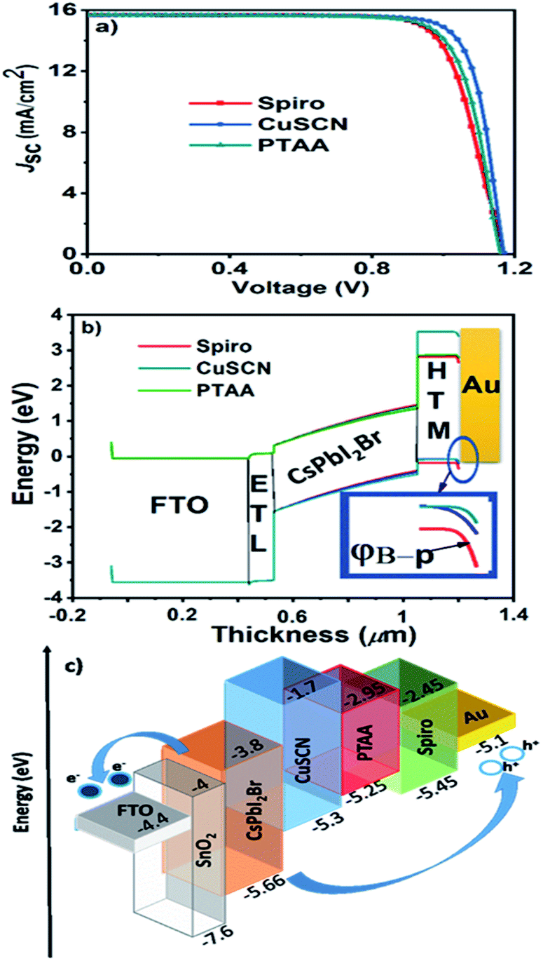 | ||
| Fig. 2 (a) J–V curves of PSCs based on different HTMs using parameters shown in Table 1, (b) corresponding energy band diagrams of the CsPbI2Br based PSCs using HTMs illustrating the energy barrier at the HTM and gold (back contact) and (c) corresponding energy band diagrams for the device structure used in the simulation. | ||
The value of the defect density for CsPbI2Br is equal to 3.64 × 1015 cm−3 which is the finest value21 while the work function of the back contact is −5.1 eV (Au). The difference in the performance between HTMs can be related to (i) the effect of the VBO and (ii) to the barrier height (ϕBp). From Table 3 we can deduce that the efficient PSCs must have balanced values between the VBO and ϕBp to facilitate the extraction of the holes from the perovskite layer and also to make an efficient transfer of the holes from the HTM to the load.
| HTMs | PCE (%) | V oc (V) | J sc (mA cm−2) | FF (%) | VBO (eV) | ϕ Bp |
|---|---|---|---|---|---|---|
| Spiro | 14.09 | 1.17 | 15.67 | 76.66 | −0.21 | −0.35 |
| PTAA | 14.28 | 1.15 | 15.67 | 79.01 | −0.41 | −0.15 |
| CuSCN | 14.90 | 1.16 | 15.68 | 81.94 | −0.36 | −0.2 |
| S–Q limit43 | 25.86 | 1.56 | 17.99 | 91.69 | — | — |
Fig. 2a and b represent the corresponding energy band diagrams of simulated PSCs with diverse HTMs. The inset depicts the formation of an “arc shaped” structure at the HTM/back contact, and this curvatures changes depending on the energy level of the valence band for each HTM that can act as a barrier to slow down the movement of holes towards the back contact. This in turn increases the recombination rate thus reducing the open circuit voltage. The Schottky contact is dominant for all three HTMs with different levels as presented with the “arc shape” (Fig. 1a).
 | (4) |
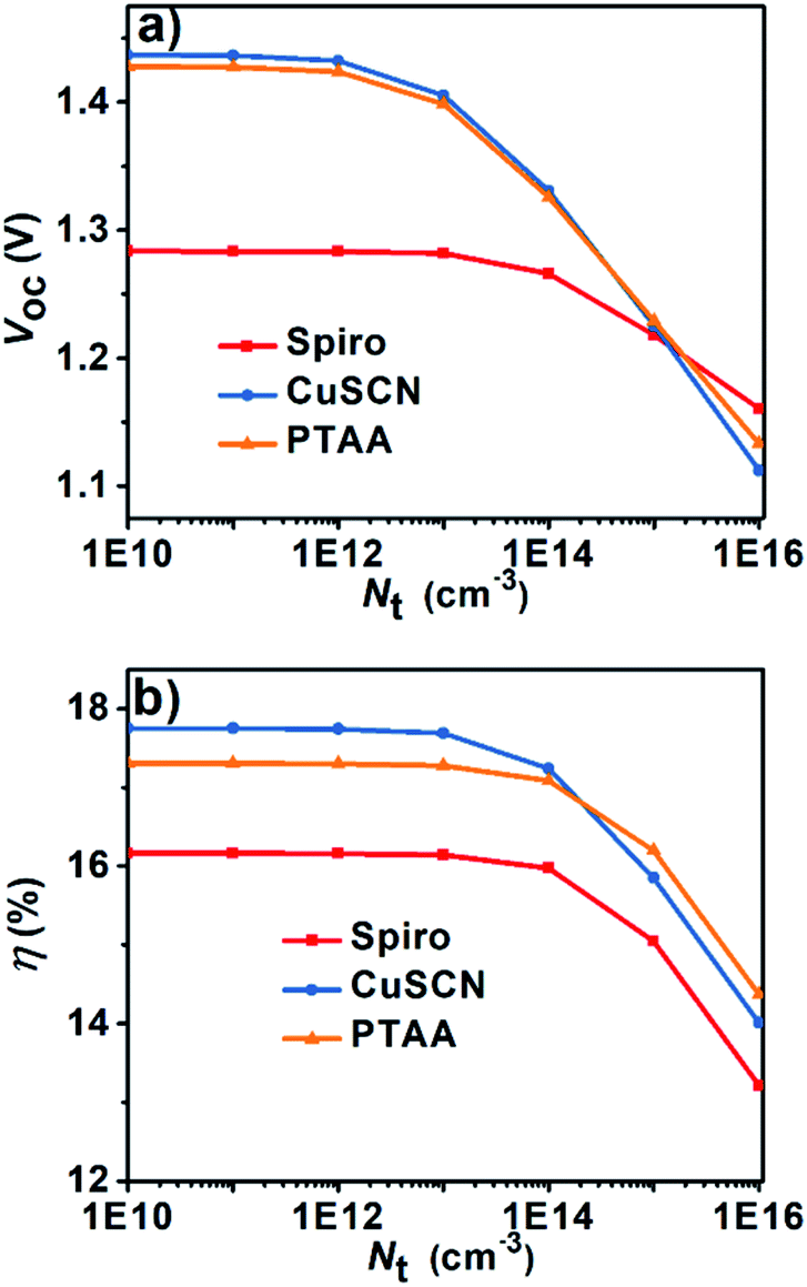 | ||
| Fig. 3 Influence of defect density in the absorber layer using different HTMs on (a) open circuit voltage and (b) efficiency. | ||
It can be deduced (Fig. 3b) that by decreasing the Nt of the absorber layer up to a certain value (Nt = 1 × 1013 cm−3), enhancement in the PCE was noted for all the HTMs studied. The lower defect density resulted in the increase of the lifetime due to the increase in the diffusion length (measure of the absorber quality) which reduces the rate of recombination.3
By comparing the PCE value (Table 3) with high defect density (3.64 × 1015 cm−3) and the optimized defect density (1 × 1013 cm−3), the increase in the PCE was noted to be 16.16, 17.44 and 17.71% for spiro-OMeTAD, PTAA and CuSCN respectively (Fig. 3b). A similar trend was observed for Voc with decreasing Nt until an optimized value of 1 × 1013 cm−3 (Fig. 3a). However, the improvement in Voc was higher in the case of CuSCN and PTAA use and 1.43 and 1.42 V respectively were achieved, compared to that for spiro-OMeTAD of 1.28 V. In the case of spiro-OMeTAD (Table 3), the VBO is lower but the barrier height is large in contrast to those of other HTMs. Taking into consideration a low defect density of the absorber layer (Nt = 1 × 1013 cm−3, for high quality layers) and a low VBO value, the theoretical value of Voc in the case of spiro-OMeTAD cannot be reached. However, if the barrier height is low with a large VBO, the performance can be close to the Shockley limit as shown for CuSCN and PTAA.
To validate these assumptions, Table 5, depicts the effect of the VBO and barrier height. The valence band energy level of spiro-OMeTAD and PTAA is optimized by varying their electron affinity and keeping it closer, to the VBO and ϕBp values of CuSCN, which can be experimentally achieved (Table 5).
| Parameter | FTO | SnO2 | IL1 | CsSnI3−xBrx | IL2 | Spiro-OMeTAD |
|---|---|---|---|---|---|---|
| Thickness (nm) | 400 | 90 | 10 | 350 | 10 | 150 |
| E g (eV) | 3.5 | 3.6 (ref. 44) | Wide range | Wide range | Wide range | 3 (ref. 37 and 38) |
| χ | 4 | 4 | 4.47 | 4.47 (ref. 47) | 4.47 | 2.45 (ref. 46) |
| ε r | 30 | 100 | 48 | 48 (ref. 48) | 48 | 3 (ref. 46) |
| N c (1 cm−3) | 2.2 × 10¹⁸ | 2.2 × 10¹⁸ | 2.2 × 10¹⁸ | 2.2 × 10¹⁸ | 2.2 × 10¹⁸ | 2.2 × 10¹⁸ |
| N v (1 cm−3) | 1.8 × 10¹⁹ | 1.8 × 10¹⁹ | 1.8 × 10¹⁹ | 1.8 × 10¹⁹ | 2.5 × 10¹⁹ | 1.8 × 10¹⁹ |
| μ n (cm2 Vs−1) | 20 | 240 (ref. 41) | 6 | 6 (ref. 33) | 6 | 2 × 10⁻³ (ref. 46) |
| μ p (cm2 Vs−1) | 10 | 240 | 6 | 6 | 6 | 2 × 10⁻³ |
| N A (1 cm−3) | — | — | 1 × 10¹³ | 1 × 10¹³ | 1 × 10¹³ | 1 × 10¹⁸ |
| N D (1 cm−3) | 2 × 10¹⁹ | 1 × 10¹⁷ | — | — | — | — |
| N t (1 cm−3) | 1 × 10¹⁵ | 1 × 10¹⁵ | Wide range | Wide range | Wide range | 1 × 10¹⁵ |
| HTMs | E v (eV) | VBO (Ev_HTM − Ev_absorber) (eV) | ϕ Bp (eV) | PCE (%) |
|---|---|---|---|---|
| Spiro-OMeTAD | −4.7 | −0.96 | −0.4 | 9.82 |
| −5 | −0.66 | −0.1 | 14.28 | |
| −5.1 | −0.56 | 0 | 15.79 | |
| −5.25 | −0.41 | −0.15 | 17.57 | |
| −5.4 | −0.26 | −0.3 | 16.29 | |
| −5.55 | −0.11 | −0.45 | 14.28 | |
| PTAA | −4.55 | −1.11 | −0.55 | 7.95 |
| −4.85 | −0.81 | −0.25 | 12.03 | |
| −5.15 | −0.51 | −0.05 | 16.52 | |
| −5.25 | −0.41 | −0.15 | 17.44 | |
| −5.3 | −0.36 | −0.2 | 17.36 | |
| −5.4 | −0.26 | −0.3 | 16.25 |
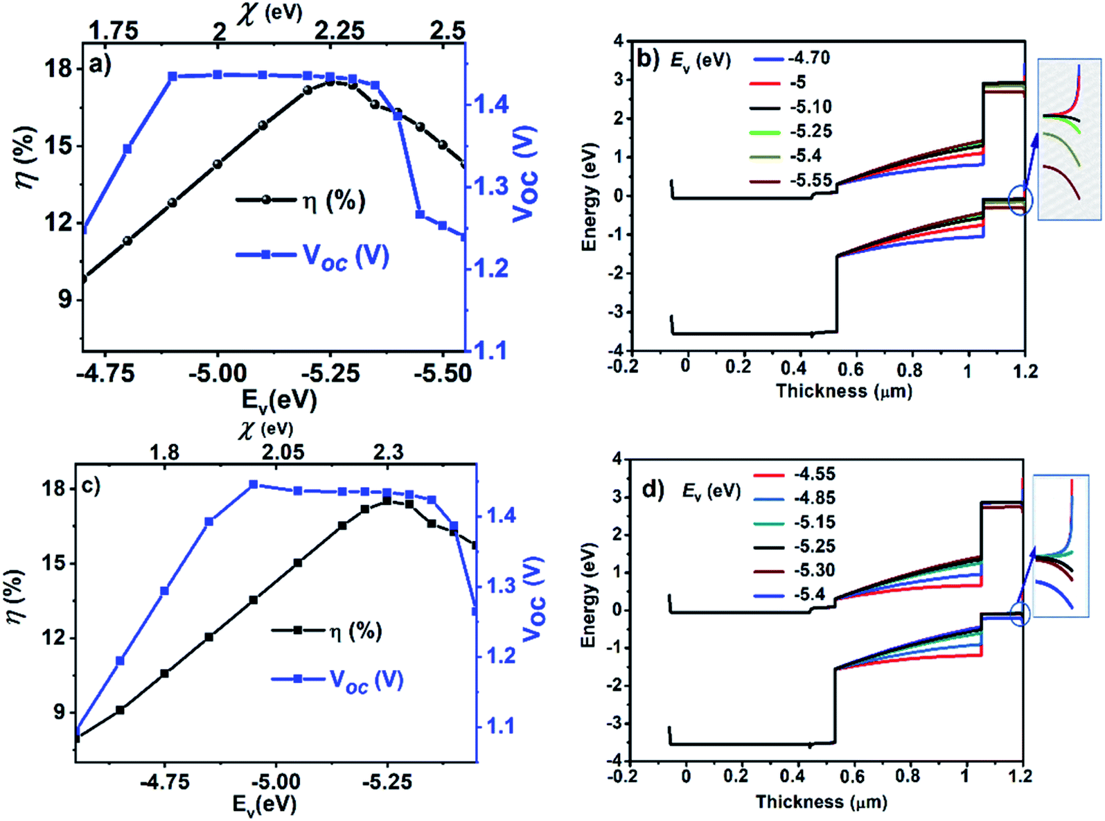 | ||
| Fig. 4 (a) Influence of the valence band of spiro-OMeTAD on the performance of CsPbI2Br PSCs, (b) corresponding energy band diagram, (c) effect of the valence band of PTAA on the performance of CsPbI2Br PSCs and (d) corresponding energy band diagram. | ||
In the context of interface engineering in optoelectronic devices, we can explain these results in two aspects, when the VBM of HTMs affects directly and/or at the same time the VBO and the barrier height (ϕBp) of the HTM–back contact affect. This implies that an optimized VBO value and ϕBp should be established for each HTM.
To further elucidate this, we analyzed the band diagram of devices with different values of Ev for each HTM (Fig. 4b and d). By changing the Ev of HTMs at the interface between the HTM and the back contact, the PCE increases with increasing the VBO value until −0.41 eV. This corresponds to the electron affinity of 2.25 and 2.3 eV for spiro and PTAA respectively, and beyond these optimized values of the VBO (corresponds to an Ev_HTM of −5.25 eV), a drop in the performance was noted due to the formation of a Schottky barrier with ϕBp for holes. The value of ϕBp was calculated using the equation described in Section 2 and increased with the increasing Ev_HTM as shown in (inset of Fig. 4b and d) Table 4. If the Schottky barrier height is greater than −0.15 eV, it will hinder the transfer of the holes to the back contact, which decreases the PCE of CsPbI2Br based PSCs. Thus the Schottky contact is preferable with a −0.15 eV barrier height. Table 6 illustrates the performance of CsPbI2Br PSCs with the optimized parameters. Nt = 1 × 1013 cm−3 for the absorber layer, VBO = −0.41 eV and (ϕBp) = −0.15 eV.
| HTMs | PCE (%) | V oc (V) | J sc (mA cm−2) | FF (%) |
|---|---|---|---|---|
| CuSCN | 17.71 | 1.43 | 15.90 | 78.90 |
| PTAA | 17.44 | 1.43 | 15.69 | 77.76 |
| Spiro | 17.57 | 1.43 | 15.69 | 78.31 |
3.2 Lead free CsSnI3−xBrx PSCs
 | ||
| Fig. 5 (a) Energy level diagram (relative to the vacuum level) of CsSnI3−xBrx by varying its electron affinity with respect to that of SnO2 as the ETL and (b) the influence. | ||
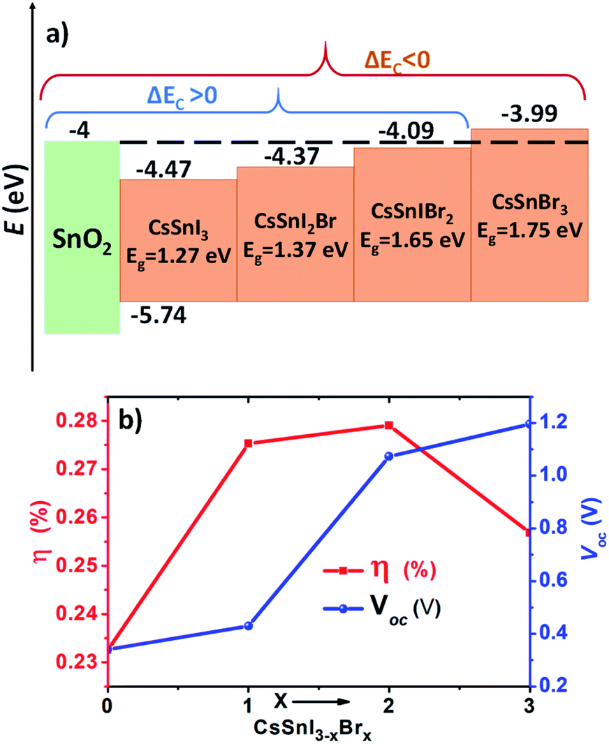
Corresponding to the Br/(I + Br) ratio, (x) ranging from 0–3, the band gap was varied from 1.27–1.75 eV (Fig. 5a). A similar trend was noted for CH3NH3PbI3 and CsSnI3,34,53 experimentally validating our investigation. The Voc increases with the increase in the band gap due to the increased Br fraction, while the PCE starts to drop beyond x = 2 (Fig. 5b). However, it reduces the absorption in the visible region. To emphasize this, here, SnO2 was employed as the ETL. The charge selective layer plays a crucial role in reducing the recombination rate and band alignments at the ETL/perovskite interface. This could be explained using the conduction band offset (CBO), i.e. the difference between the conduction band minimum (CBM) of the ETL and those of the perovskite layer (±ΔEc),54 and the (+) sign represents the spike structure and the (−) sign represents the cliff structure.35 The spike structure is shown to be favorable for improving the performance of PSCs, which can build a potential barrier at the ETL/perovskite to reduce the recombination rate.55
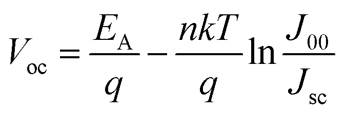
From our theoretical and experimental observation, with the increase in the band gap of perovskites, only Ec is assumed to shift upwards and thus, the CBO becomes smaller with an optimum value of +0.09 eV (spike structure) for CsSnIBr2 and gives the best performance (Fig. 5a). The PCE decreases significantly after x = 2 and the Voc can be described by the following equation.56,57
V oc is open circuit voltage, EA is activation energy, n is the diode ideality factor, K is the Boltzmann constant, T is the temperature, J00 is the current prefactor and Jsc is the short circuit current density. For T = 0 K, and Voc = EA/q, the CBM of bulk CsSnI3 compared to the CBM of the ETL is much deeper; thus a large energy barrier with ΔEc = +0.47 eV affects the performance of the PSC. By adding Br to the CsSnI3 the band gap increases by shifting the conduction band upwards. This enhances the energy level with the ETL and the ΔEc becomes small enough to facilitate the transfer of electrons toward the front side of the load with the increase of the activation energy as well as Voc. The performance of our first model using CsSnIBr2 is still low and matches with the experimental finding, which can be ascribed to the high defect density in the absorber and at the selective layer interfaces.
 | (5) |
| EA = Eg − ΔEc | (6) |
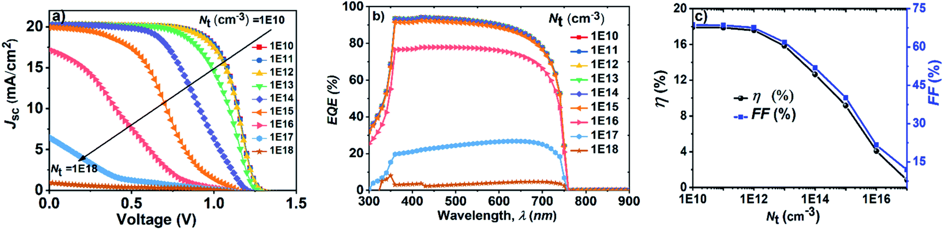 | ||
| Fig. 6 Influence of the defect density in the absorber layer on (a) J–V curve, (b) the external quantum efficiency and (c) efficiency and fill factor. | ||
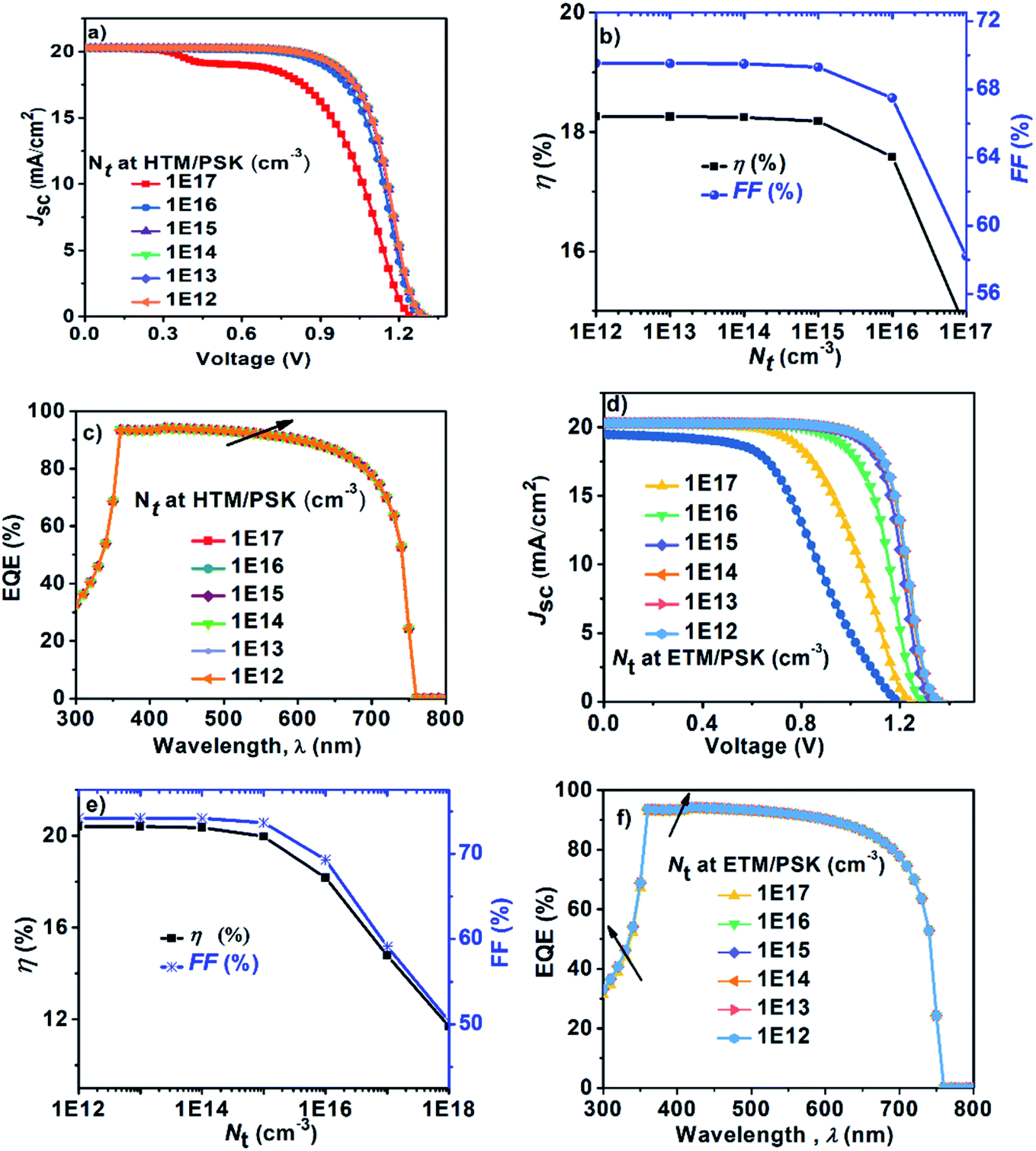 | ||
| Fig. 7 Influence of the defect density at the CsSnIBr2/HTM on (a) J–V curve, (b) efficiency and fill factor and (c) the external quantum efficiency and influence of the defect density at ETM/CsSnIBr2 on (d) J–V curve, (e) efficiency and fill factor and (f) the external quantum efficiencies. | ||
 | (7) |
 | (8) |
 | (9) |
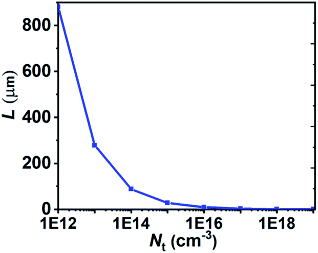 | ||
| Fig. 8 Carrier diffusion length as a function of defect density in our modelled inorganic CsSnIBr2 based PSC. | ||
As discussed (Section 3.2), PSCs based on the n–i–p configuration, FTO/SnO2/CsSnIBr2/spiro-OMeTAD/Au were optimized through studying the impact of defect density in CsSnIBr2 and at its interfaces. By using the optimum values of the defect densities for CsSnIBr2 (1012 cm−3), CsSnIBr2/HTM (1015 cm−3) and ETM/CsSnIBr2 (1014 cm−3) respectively, we can estimate a value of 278 μm as the diffusion length for the charge carriers in the absorber layer, and 27.84 μm and 88.06 μm in the case of CsSnIBr2/HTM and ETM/CsSnIBr2 interface layers respectively. Further using these optimum values of Nt, a theoretical value of PCE = 20.32%, Voc = 1.35 V, Jsc = 20.30 mA cm−2 and FF of 74.17% can be achieved (Table 7).
The Table 7 summarizes the experimental studies reported and compared to our first model and the optimized model. The optimized model shows promising results in the field of lead-free inorganic PSCs close to the Shockley–Queisser-limit.43 Adopting a new experimental protocol for syntheses of tin based materials in a Pyrex-tube at high temperature under vacuum can avoid the oxidation and improve the quality (crystallinity) of the absorber to harvest additional light with low defect density.62 Further, the passivation mechanism could be a helpful strategy to minimize the trap density at the interfaces of selective layers.
4. Conclusions
To summarize, using a one dimensional computational approach, the device structure of FTO/SnO2/CsPbI2Br/HTMs/Au was designed by selecting different organic, polymeric and inorganic hole transport materials such as spiro-OMeTAD, PTAA and CuSCN. The defect density of the absorber layer has significant influence on the performance of PSCs. Tuning the valence band maximum of spiro-OMeTAD and PTAA gave a high performance as compared to that for CuSCN. An optimized value of the VBO (−0.41 eV) and the barrier height between the HTM and back contact (−0.15 eV) with the Schottky contact was noted to be beneficial to achieve high performance. We further studied lead free inorganic PSCs based on CsSnI3−xBrx and found that the addition of Br to substitute I in CsSnI3 also allows the improvement of the band alignment with the ETL. The quality of the absorber layer and its interface is paramount to design efficient inorganic Pb-free PSCs that can be controlled by optimizing the defect density. We put forward the design of high performance Pb-free PSCs having the structure of FTO/SnO2/CsSnIBr2/spiro-OMeTAD/Au, with Nt = 1012 cm−3 for the absorber layer, Nt = 1015 cm−3 in the case of the CsSnIBr2/HTM and Nt = 1014 cm−3 for the ETM/CsSnIBr2 yielding a PCE of 20.32%. Our computational approach can pave the way to boost the performance of inorganic Pb and Pb-free PSCs by taking into account the developed parameters.Conflicts of interest
There are no conflicts to declare.Acknowledgements
This work has received funding from the European Union H2020 Programme under European Research Council Consolidator grant [MOLEMAT, 726360] and PARASOL (RTI2018-102292-B-I00) from Spanish Ministry of Science and Innovation. The authors would like to thank Professor Marc Burgelman, Department of Electronic and Information Systems, University of Gent for the development of the SCAPS software package and allowing its use.References
- S. Kazim, M. K. Nazeeruddin, M. Graetzel and S. Ahmad, Angew. Chem., Int. Ed., 2014, 53, 2812–2824 ( Angew. Chem. , 2014 , 126 , 2854–2867 ) CrossRef CAS.
- J. Huang, Y. Yuan, Y. Shao and Y. Yan, Nat. Rev. Mater., 2017, 2, 17042 CrossRef CAS.
- L. Calió, S. Kazim, M. Grätzel and S. Ahmad, Angew. Chem., Int. Ed., 2016, 55, 14522–14545 ( Angew. Chem. , 2016 , 128 , 14740–14764 ) CrossRef.
- S. Kazim, F. J. Ramos, P. Gao, M. K. Nazeeruddin, M. Grätzel and S. Ahmad, Energy Environ. Sci., 2015, 8, 1816–1823 RSC.
- A. Kojima, K. Teshima, Y. Shirai and T. Miyasaka, J. Am. Chem. Soc., 2009, 131, 6050–6051 CrossRef CAS.
- J.-P. Correa-Baena, M. Saliba, T. Buonassisi, M. Grätzel, A. Abate, W. Tress and A. Hagfeldt, Science, 2017, 358, 739–744 CrossRef CAS.
- G. Bai, Z. Wu, J. Li, T. Bu, W. Li, W. Li, F. Huang, Q. Zhang, Y. B. Cheng and J. Zhong, Sol. Energy, 2019, 183, 306–314 CrossRef CAS.
- M. Lazemi, S. Asgharizadeh and S. Bellucci, Phys. Chem. Chem. Phys., 2018, 20, 25683–25692 RSC.
- N. J. Jeon, J. H. Noh, W. S. Yang, Y. C. Kim, S. Ryu, J. Seo and S. Il Seok, Nature, 2015, 517, 476–480 CrossRef CAS.
- W. Travis, E. N. K. Glover, H. Bronstein, D. O. Scanlon and R. G. Palgrave, Chem. Sci., 2016, 7, 4548–4556 RSC.
- M. A. Green, A. Ho-Baillie and H. J. Snaith, Nat. Photonics, 2014, 8, 506–514 CrossRef CAS.
- M. Kulbak, S. Gupta, N. Kedem, I. Levine, T. Bendikov, G. Hodes and D. Cahen, J. Phys. Chem. Lett., 2016, 7, 167–172 CrossRef CAS.
- A. Marronnier, G. Roma, S. Boyer-Richard, L. Pedesseau, J. M. Jancu, Y. Bonnassieux, C. Katan, C. C. Stoumpos, M. G. Kanatzidis and J. Even, ACS Nano, 2018, 12, 3477–3486 CrossRef CAS.
- R. J. Sutton, G. E. Eperon, L. Miranda, E. S. Parrott, B. A. Kamino, J. B. Patel, M. T. Hörantner, M. B. Johnston, A. A. Haghighirad, D. T. Moore and H. J. Snaith, Adv. Energy Mater., 2016, 6, 1502458 CrossRef.
- W. Chen, H. Chen, G. Xu, R. Xue, S. Wang, Y. Li and Y. Li, Joule, 2019, 3, 191–204 CrossRef CAS.
- H. Rao, S. Ye, F. Gu, Z. Zhao, Z. Liu, Z. Bian and C. Huang, Adv. Energy Mater., 2018, 8, 1800758 CrossRef.
- W. Chen, H. Chen, G. Xu, R. Xue, S. Wang, Y. Li and Y. Li, Joule, 2019, 3, 191–204 CrossRef CAS.
- L. Yan, Q. Xue, M. Liu, Z. Zhu, J. Tian, Z. Li, Z. Chen, Z. Chen, H. Yan, H.-L. Yip and Y. Cao, Adv. Mater., 2018, 30, 1802509 CrossRef.
- Y. Raoui, H. Ez-Zahraouy, N. Tahiri, O. El Bounagui, S. Ahmad and S. Kazim, Sol. Energy, 2019, 193, 948–955 CrossRef CAS.
- Q. Zeng, X. Zhang, C. Liu, T. Feng, Z. Chen, W. Zhang, W. Zheng, H. Zhang and B. Yang, Sol. RRL, 2019, 3, 1800239 CrossRef.
- G. Yin, H. Zhao, H. Jiang, S. Yuan, T. Niu, K. Zhao, Z. Liu and S. (Frank) Liu, Adv. Funct. Mater., 2018, 28, 1803269 CrossRef.
- Y. Han, H. Zhao, C. Duan, S. Yang, Z. Yang, Z. Liu and S. (Frank) Liu, Adv. Funct. Mater., 2020, 1909972 CrossRef CAS.
- B. Saparov, J. P. Sun, W. Meng, Z. Xiao, H. S. Duan, O. Gunawan, D. Shin, I. G. Hill, Y. Yan and D. B. Mitzi, Chem. Mater., 2016, 28, 2315–2322 CrossRef CAS.
- W. J. Yin, T. Shi and Y. Yan, J. Phys. Chem. C, 2015, 119, 5253–5264 CrossRef CAS.
- W. J. Yin, T. Shi and Y. Yan, Adv. Mater., 2014, 26, 4653–4658 CrossRef CAS.
- P. Huang, S. Kazim, M. Wang and S. Ahmad, ACS Energy Lett., 2019, 4, 2960–2974 CrossRef CAS.
- F. Hao, C. C. Stoumpos, D. H. Cao, R. P. Chang and M. G. Kanatzidis, Nat. Photonics, 2014, 8, 489–494 CrossRef CAS.
- A. C. Grimsdale, T. M. Koh, T. Krishnamoorthy, N. Yantara, C. Shi, W. L. Leong, P. P. Boix, S. G. Mhaisalkar and N. Mathews, J. Mater. Chem. A, 2015, 3, 14996–15000 RSC.
- R. Wang, M. Mujahid, Y. Duan, Z.-K. Wang, J. Xue and Y. Yang, Adv. Funct. Mater., 2019, 1808843 CrossRef CAS.
- Z. Chen, J. J. Wang, Y. Ren, C. Yu and K. Shum, Appl. Phys. Lett., 2012, 101, 093901 CrossRef.
- I. Chung, J. H. Song, J. Im, J. Androulakis, C. D. Malliakas, H. Li, A. J. Freeman, J. T. Kenney and M. G. Kanatzidis, J. Am. Chem. Soc., 2012, 134, 8579–8587 CrossRef CAS.
- K. P. Marshall, M. Walker, R. I. Walton and R. A. Hatton, J. Mater. Chem. A, 2017, 5, 21836–21845 RSC.
- M. H. Kumar, S. Dharani, W. L. Leong, P. P. Boix, R. R. Prabhakar, T. Baikie, C. Shi, H. Ding, R. Ramesh, M. Asta, M. Graetzel, S. G. Mhaisalkar and N. Mathews, Adv. Mater., 2014, 26, 7122–7127 CrossRef CAS.
- D. Sabba, H. K. Mulmudi, R. R. Prabhakar, T. Krishnamoorthy, T. Baikie, P. P. Boix, S. Mhaisalkar and N. Mathews, J. Phys. Chem. C, 2015, 119, 1763–1767 CrossRef CAS.
- Y. Raoui, H. Ez-Zahraouy, S. Kazim and S. Ahmad, J. Energy Chem., 2021, 54, 822–829 CrossRef.
- D. A. Neamen, Semiconductor Physics and Devices Basic Principles, 4th edn, McGraw-Hill, New York NY, 2012 Search PubMed.
- J. Zhuang, Y. Wei, Y. Luan, N. Chen, P. Mao, S. Cao and J. Wang, Nanoscale, 2019, 11, 14553–14560 RSC.
- J. Wang, W. Fu, S. Jariwala, I. Sinha, A. K. Y. Jen and D. S. Ginger, ACS Energy Lett., 2019, 4, 222–227 CrossRef CAS.
- K. Masumura, I. Nakanishi, K. Van Thi Khuat, K. Kinashi, W. Sakai and N. Tsutsumi, Sci. Rep., 2019, 9, 1–9 CrossRef CAS.
- X. Meng, Z. Wang, W. Qian, Z. Zhu, T. Zhang, Y. Bai, C. Hu, S. Xiao, Y. Yang and S. Yang, J. Phys. Chem. Lett., 2018, 10, 194–199 CrossRef.
- H. J. Snaith and C. Ducati, Nano Lett., 2010, 10, 1259–1265 CrossRef CAS.
- H. Zai, D. Zhang, L. Li, C. Zhu, S. Ma, Y. Zhao, Z. Zhao, C. Chen, H. Zhou, Y. Li and Q. Chen, J. Mater. Chem. A, 2018, 6, 23602–23609 RSC.
- S. Rühle, Sol. Energy, 2016, 130, 139–147 CrossRef.
- T. J. Barr, R. N. Sampaio, B. N. DiMarco, E. M. James and G. J. Meyer, Chem. Mater., 2017, 29, 3919–3927 CrossRef CAS.
- W. Shockley and W. T. Read, Phys. Rev., 1952, 87, 835–842 CrossRef CAS.
- T. Minemoto and M. Murata, J. Appl. Phys., 2014, 116, 054505 CrossRef.
- J. Zhang, C. Yu, L. Wang, Y. Li, Y. Ren and K. Shum, Sci. Rep., 2014, 4, 6954 CrossRef CAS.
- L. Y. Huang and W. R. L. Lambrecht, Phys. Rev. B: Condens. Matter Mater. Phys., 2013, 88, 1–12 Search PubMed.
- S. Selberherr and S. Selberherr, The Physical Parameters. Analysis and Simulation of Semiconductor Devices, Springer Vienna, Vienna, 1984, pp. 80–126 Search PubMed.
- W. Shockley and W. T. Read, Phys. Rev., 1952, 87, 835–842 CrossRef CAS.
- S. Heo, G. Seo, Y. Lee, D. Lee, M. Seol, J. Lee, J. B. Park, K. Kim, D. J. Yun, Y. S. Kim, J. K. Shin, T. K. Ahn and M. K. Nazeeruddin, Energy Environ. Sci., 2017, 10, 1128–1133 RSC.
- J. M. Ball and A. Petrozza, Nat. Energy, 2016, 1, 1–13 Search PubMed.
- S. A. Kulkarni, T. Baikie, P. P. Boix, N. Yantara, N. Mathews and S. Mhaisalkar, J. Mater. Chem. A, 2014, 2, 9221–9225 RSC.
- T. Minemoto and M. Murata, Sol. Energy Mater. Sol. Cells, 2015, 133, 8–14 CrossRef CAS.
- C. Ding, Y. Zhang, F. Liu, Y. Kitabatake, S. Hayase, T. Toyoda, K. Yoshino, T. Minemoto, K. Katayama and Q. Shen, Nano Energy, 2018, 53, 17–26 CrossRef CAS.
- T. H. Lai, S. W. Tsang, J. R. Manders, S. Chen and F. So, Mater. Today, 2013, 16, 424–432 CrossRef CAS.
- K. Tvingstedt and C. Deibel, Adv. Energy Mater., 2016, 6, 1502230 CrossRef.
- S. Z. Haider, H. Anwar, Y. Jamil and M. Shahid, J. Phys. Chem. Solids, 2020, 136, 109147 CrossRef CAS.
- P. W. Liang, C. Y. Liao, C. C. Chueh, F. Zuo, S. T. Williams, X. K. Xin, J. Lin and A. K. Y. Jen, Adv. Mater., 2014, 26, 3748–3754 CrossRef CAS.
- L. Li, Y. Chen, Z. Liu, Q. Chen, X. Wang and H. Zhou, Adv. Mater., 2016, 28, 9862–9868 CrossRef CAS.
- D. Bi, C. Yi, J. Luo, J. D. Décoppet, F. Zhang, S. M. Zakeeruddin, X. Li, A. Hagfeldt and M. Grätzel, Nat. Energy, 2016, 1, 16142 CrossRef CAS.
- M. Chen, M.-G. Ju, H. F. Garces, A. D. Carl, L. K. Ono, Z. Hawash, Y. Zhang, T. Shen, Y. Qi, R. L. Grimm, D. Pacifici, X. C. Zeng, Y. Zhou and N. P. Padture, Nat. Commun., 2019, 10, 16 CrossRef CAS.
| This journal is © The Royal Society of Chemistry 2021 |