
 Open Access Article
 This Open Access Article is licensed under a Creative Commons Attribution-Non Commercial 3.0 Unported Licence
Au nanolenses for near-field focusing†
Sungwoo
Lee‡
a,
Soohyun
Lee‡
a,
Jae-Myoung
Kim
b,
Jiwoong
Son
b,
Eunbyeol
Cho
a,
Sungjae
Yoo
a,
Hajir
Hilal
a,
Jwa-Min
Nam
 b and
Sungho
Park
*a
b and
Sungho
Park
*a
aDepartment of Chemistry, Sungkyunkwan University, Suwon 440-746, South Korea. E-mail: spark72@skku.edu
bDepartment of Chemistry, Seoul National University, Seoul, 08826, South Korea
First published on 26th March 2021
Abstract
We report a novel strategy for the synthesis of Pt@Au nanorings possessing near-field focusing capabilities at the center through which single-particle surface enhanced Raman scattering could be readily observed. We utilized Pt@Au nanorings as a light-absorber; the absorbed light could be focused at the center with the aid of a Au nanoporous structure. We synthesized the Au nanolens structure through a Galvanic exchange process between Au ions and Ag block at the inner domain of the Pt@Au nanoring. For this step, Ag was selectively pre-deposited at the inner domain of the Pt@Au nanorings through electrochemical potential-tuned growth control and different surface energies with regard to the inner and outer boundaries of the nanoring. Then, the central nanoporous architecture was fabricated through the Galvanic exchange of sacrificial Ag with Au ions leading to the resulting Au nanoring with a Au nanoporous structure at the center. We monitored the shape-transformation by observing their corresponding localized surface plasmon resonance (LSPR) profiles. By varying the rim thickness of the starting Pt@Au nanorings, the inner diameter of the nanolens was accordingly tuned to maximize near-field focusing, which enabled us to obtain the reproducible and light-polarization independent measurements of single-particle SERS. Through theoretical simulation, the near-field electromagnetic field focusing capability was visualized and confirmed through single-particle SERS measurement showing an enhancement factor of 1.9 × 10⁸ to 1.0 × 10⁹.
Introduction
Localized surface plasmon resonance (LSPR) is a distinctive optical property of noble metallic nanoparticles (Au, Ag, or Cu nanoparticles) and is the collective oscillation of conduction electrons driven by irradiated electromagnetic waves at the surface of noble metal nanoparticles, enabling the utilization of noble metal nanoparticles for surface-enhanced Raman scattering (SERS) application.1,2 SERS is a powerful analytical technique providing ultrasensitive analysis at the single-molecule scale, which can be widely applied toward life science, chemical production, and environmental monitoring.3–7 It is now well understood that surface plasmons of noble metal nanoparticles, particularly at the narrow gaps or junctions between nanoparticles, localize and enhance the E-field near noble metal nanoparticles (referred to as “hot spots”) for amplifying the Raman scattering of target molecules.8–11To generate hotspots, nanostructures with interparticle gaps,12–14 intraparticle gaps,15–21 sharp tips,22–24 or rough surfaces25,26 were synthesized. Nanoparticles with intraparticle gaps have attracted considerable attention due to their homogeneity and tunability in hotspots, leading to enhanced SERS signal sensitivity and reproducibility.27–29 To fabricate nanostructures with intraparticle gaps, several synthetic strategies have been utilized: (1) the utilization of thiolated DNA to synthesize core–shell nanostructures,16,30 (2) the employment of polymer shells to fabricate long narrow junctions,17,31 and (3) porous structure formation through plasma-etching or dealloying with acids.32,33 In particular, porous Au nanoparticles were synthesized and utilized due to their large surface-to-volume ratio and high density of nanogaps, which enabled us to apply them to catalysis or SERS application.34–36 Nanorings were synthesized through several approaches including template-based synthesis and colloidal lithography.37,38 In a previous study, we reported Ag double nanorings for efficient single-particle SERS.19
Herein, we suggest a novel methodology for synthesizing Au nanolens nanostructures with a central “hot area” within a single entity. We synthesized Au nanolens structure by integrating Au nanoporous structure at the inner domain of a Pt@Au nanoring through an eccentric growth of Ag, and a subsequent nanoscale Galvanic exchange reaction. We adopted Pt nanorings as a rigid skeleton for Au wrapping and the resulting Au nanorings later played a role as a light absorber. The absorbed light was concentrated at the center with the aid of a central porous Au nanostructure, allowing for near-field electromagnetic focusing whose intensity varied as a function of rim-thickness and inner diameter of the Au nanorings. The resulting Au nanolens exhibited strong and uniform single-particle SERS signal, which was independent to incident light polarization.
Results and discussion
As represented in Scheme 1, we suggested an on-demand and multi-stepwise synthetic procedure for Au nanolenses. In our previous reports, we established unique synthetic pathways leading to circular Au nanorings.37 In the current work, we systematically varied the rim-thickness of Au nanorings and found a way to selectively deposit Ag within the inner domain of Au nanorings, namely in an eccentric fashion. The overall synthetic procedure is composed of six steps: (1) selective etching of Au, (2) rim-on deposition of Pt, (3) selective etching of Au, (4) concentric growth of Au, (5) eccentric growth of Ag, and (6) nanoscale Galvanic exchange reactions. It was noteworthy that the proposed synthetic strategy was highly efficient such that the resulting final product showed high homogeneity (∼90%) with regard to both size and shape. Briefly, we first synthesized Au nanoprisms (edge length ∼143 (±10) nm) as a starting material. In step 1 (selective etching of Au), we selectively etched the vertex sites of Au nanoprisms using Au3+ ions, inducing a shape transformation to Au nanodisks. The protruding tips were labile to the chemical etching environment because vertex sites (coordination number ≈ 6) have higher surface energy compared to flat terrace sites (coordination number ≈ 9). In step 2 (rim-on deposition of Pt), Pt rims were formed around the periphery of the Au nanodisks and were referred to as Au@Pt nanodisks. A detail mechanism for the chemical reaction has already been described in our previous literatures.37,39,40 In step 3 (selective etching of Au), we selectively etched inner gold using Au3+ ions through a comproportionation reaction (AuCl4− + 2Au + 2Cl− → 3AuCl2−), leading to Pt nanorings. In step 4 (concentric growth of Au), we wrapped the Pt rims with Au through the reduction of Au3+ ions using ascorbic acid, resulting in Pt@Au nanorings. The rim thickness of the Pt@Au nanorings was easily tuned by varying the total amount of Au3+ precursors during the Au deposition step.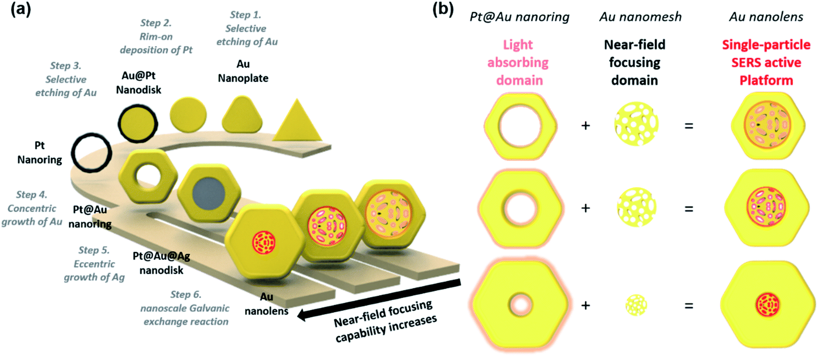 | ||
| Scheme 1 (a) Schematic illustration of a synthetic procedure for synthesizing Au nanolenses. The multistep synthetic procedure to synthesize Au nanolens structures included the selective etching of Au, rim-on deposition of Pt, selective etching of Au, concentric growth of Au, eccentric growth of Ag, and Galvanic exchange. (b) The Au nanolens structure is a single-particle SERS active platform with the support of both Pt@Au nanorings (light absorbing domain) and Au nanoporous structure (near-field focusing domain). | ||
In step 5 (eccentric growth of Ag), we asymmetrically reduced Ag+ ions on the Pt@Au nanorings in an eccentric growth pattern. It was noteworthy that this asymmetric growth was a key step toward constructing the final Au nanolenses. The controlled growth of Ag was achieved by tuning the standard reduction potential of Ag+ with halide counter ions. Under slow kinetic growth condition by adopting Br− ions (E°[AgBr/Ag] = 0.07 V), Ag+ ions were preferentially reduced at the inner periphery, which was driven by the high surface energy of the inner periphery compared to the outer boundary. The Au nanorings with empty inner holes exhibit structural differences between the inner and outer boundaries. The shape of the inner boundary was close to the circle, whereas the outer boundaries exhibited hexagonal shapes. This indicated that the inner boundaries were composed of higher index crystalline facets, implying the higher reactivity of inner boundary compared to the outer peripheries. When the driving electrochemical potential (ΔE) was higher than both Eouter-boundary and Einner-boundary, the Ag deposition on the inner and outer boundaries would occur simultaneously. By contrast, if the ΔE was in-between Eouter-boundary and Einner-boundary, the preferential growth of Ag on the inner-boundary would be expected. When Br− ions were adopted as counter ions (E°[AgBr/Ag] = 0.07 V), the estimated ΔE was ca. 0.04 V under the given experimental condition, leading to eccentric Ag growth. By contrast, when Cl− ions were employed, ΔE was ca. 0.19 V, leading to concentric Ag growth.
Finally, in step 6 (nanoscale Galvanic exchange reaction), we transformed the inner Ag domain into a Au nanoporous structure through a “nanoscale Galvanic exchange reaction” between Au3+ ions and sacrificial Ag blocks. First, a thin Au layer was formed on the surface of the Ag domain because there was a difference in the redox potentials of AuCl4−/Au and Ag+/Ag allowing oxidation of the Ag layer and reduction of Au3+ ions.41 As the Galvanic exchange reaction proceeded, voids were generated on the surface of the Ag template because three Ag atoms were oxidized for the reduction of one Au3+ ion. As a result, the extraction of more Ag than the replacement by Au proceeded and pores were continually formed. Additionally, surface rearrangement occurred in a way that Ag covered the surface as the dominant surface species due to the lower surface energy of Ag than Au.42 The exposed Ag continued to be replaced with Au, leading to transformation of the nanoporous network at the center; we named the entire structure as Au nanolenses. It was noteworthy that the outer circular Pt@Au skeleton was rigid enough to hold the central Au nanoporous structure without collapsing. The presence or absence of the central Au nanoporous structure largely affected the focusing ability of the electric near-field.
Typically, we prepared Pt nanorings by following our previously reported protocol ((1) selective etching of Au, (2) rim-on deposition of Pt, and (3) selective etching of Au).37 The field-emission scanning electron microscopy (FE-SEM) images (ESI, Fig. S1a–d,† and 1a) represented the homogeneous size and shape distribution of the resulting Au nanoprisms, Au nanodisks, Au@Pt nanodisks, and Pt nanorings, respectively. By following the schematic synthetic routes of Scheme 1, we successfully synthesized homogenous Pt@Au nanorings (Fig. 1b), Pt@Au@Ag nanodisks (Fig. 1c), and Au nanolenses (Fig. 1d–f). The size distribution histogram of the Pt@Au nanorings showed that the rim thickness was 45 (±6) nm and the diameter was 142 (±8) nm (Fig. S2a†). After we asymmetrically deposited Ag onto the Pt@Au nanorings in the presence of hexadecyltrimethyl ammonium bromide (CTAB), there was no noticeable change in diameter (from 142 (±8) nm to 143 (±9) nm) as shown in the size distribution analysis (Fig. S2b†), indicating the eccentric growth of Ag in the inner-wards. It was clearly noticeable through the contrast difference between the dark inner domains (light Ag atoms) and bright-colored circular nanorings (heavier Au atoms) as shown in Fig. 1c. The corresponding EDS mapping and line mapping analysis showed that the central block was composed of pure Ag and there was little Ag presence at the rims (panels j and k). By contrast, when we deposited Ag on the Pt@Au nanorings in the presence of chloride ions (which was a concentric growth mode), we observed the homogeneous growth of Ag around the Pt@Au nanorings and a concomitant increase in rim thickness to 49 (±6) nm (Fig. S3†).
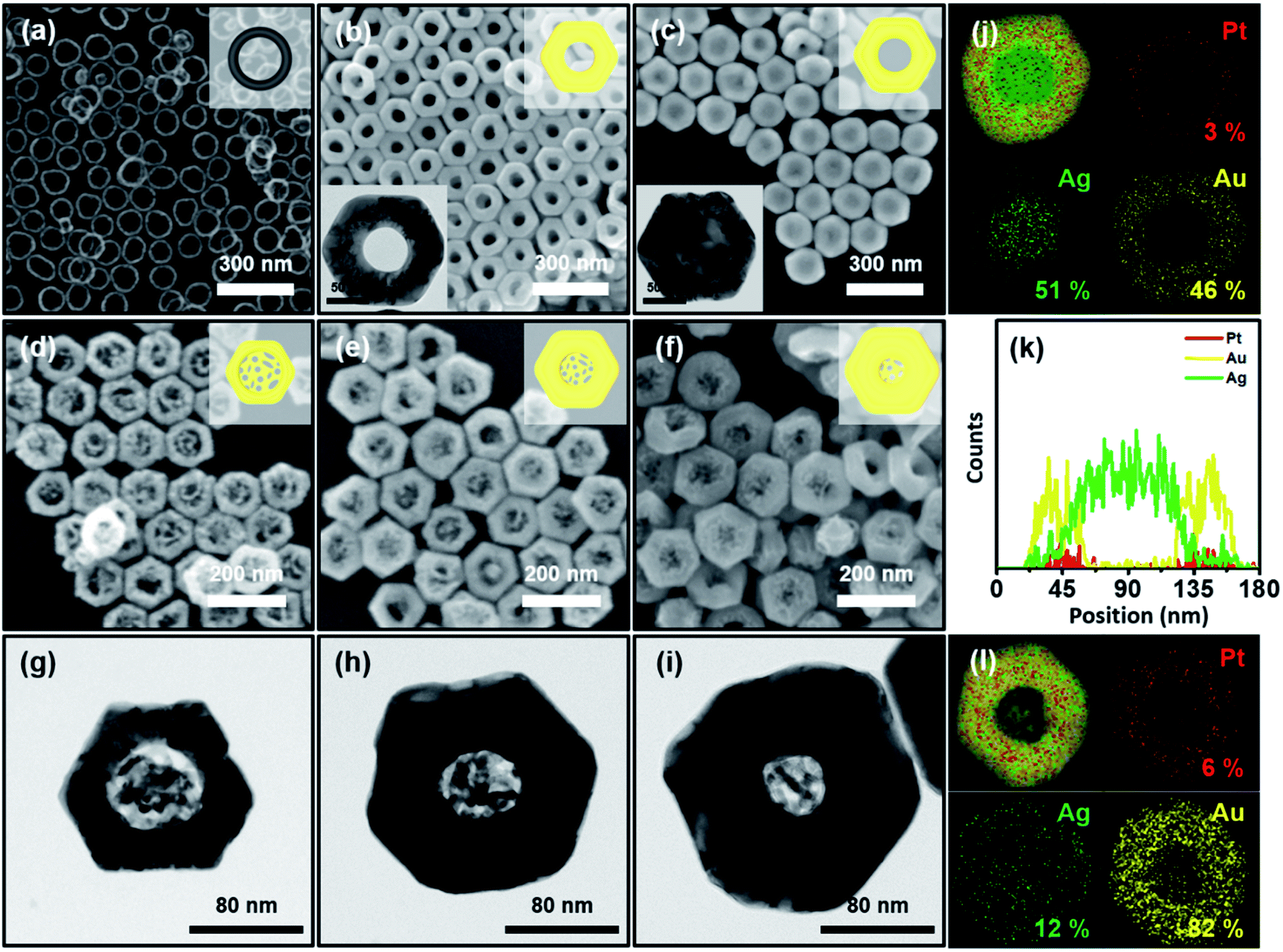 | ||
| Fig. 1 Field-emission scanning electron microscopy (FE-SEM) images of (a) Pt nanorings, (b) Pt@Au nanorings, (c) Pt@Au@Ag nanodisks, and (d–f) Au nanolenses. (g–i) High-resolution transmission electron microscopy (HR-TEM) images of Au nanolenses shown in (d–f), respectively. (j) Energy dispersive spectroscopy (EDS) elemental mapping image and (k) EDS line mapping data of a Pt@Au@Ag nanodisk. (l) An EDS elemental mapping image of an Au nanolens nanoparticle. | ||
After we performed the Galvanic exchange reaction with Au3+ ions, the central Ag blocks transformed into a nanoporous network of Au, which was represented by dark semi-transparent blocks at the center in Fig. 1d–f (Fig. S4†). We prepared two other analogous Au nanolenses with larger inner diameters (∼58 nm in panel d) and a smaller one (∼35 nm in panel f). The rim thickness of each sample (panel d, e, and f) was 30 (±3), 44 (±4), and 60 (±6) nm, respectively. The close zoomed-in TEM analysis clearly showed that the solid Au rims wrapped the inner nanoporous blocks (Fig. 1g–i). The ligaments of the nanoporous structure were intertwined and the outer regions were connected to the Au rims. The corresponding EDS mapping image revealed that the outer surface was mainly composed of Au, Pt was embedded in the Au rim, and a small amount of Ag was scattered over the entire surface (Fig. 1l).
Of critical interest was a comparison of the UV-visible-NIR spectrum obtained following each shape evolution (Fig. 2a). The localized surface plasmon resonance (LSPR) profile of the as-prepared Au nanorings (diameter ∼142 nm & rim-thickness ∼45 nm) showed a distinct in-plane dipole mode at 841 nm and an out-of-plane dipole mode at 510 nm (black trace). After growing Ag in an eccentric mode and filling the center, the in-plane mode blue shifted to 648 nm (red trace). As expected, there was another band appearing at 374 nm, which was the characteristic LSPR dipole mode of the Ag blocks. As the central solid Ag blocks transformed into a nanoporous structure, the in-plane mode redshifted to 811 nm and the out-of-plane mode shifted to 560 nm (blue trace). Furthermore, we can analyze plasmonic modes based on the hybridization model.43 The hybridization of plasmonic mode of ring structure and porous structure leads to the generation of bonding plasmonic mode (811 nm, lower energy) and antibonding plasmonic mode (560 nm, higher energy). Increase in rim thickness of Au nanolens structure leads to change in resonance condition of nanostructure, which results in the blueshift of bonding mode and the redshift of antibonding mode. The disappearance of Ag was clearly noticeable with spectral profiles, which was represented by the disappearance of the band at 374 nm. One noticeable feature was the absence of the out-of-plane mode with the thinnest rims because of the low Au mass of nanostructure (pink trace). For theoretical calculation, we adopted the model with arrays of pillars at the center of Au nanorings, leading to the good agreement of the experimental observation. In contrast, when we applied the void-area dominant nanoporous network at the center for the simulation, the simulation predicted the opposite trend to the experimental results. Therefore, it is obvious that the central region is the solid-area dominant nanoporous network, which is effective for near-field focusing (vide infra).
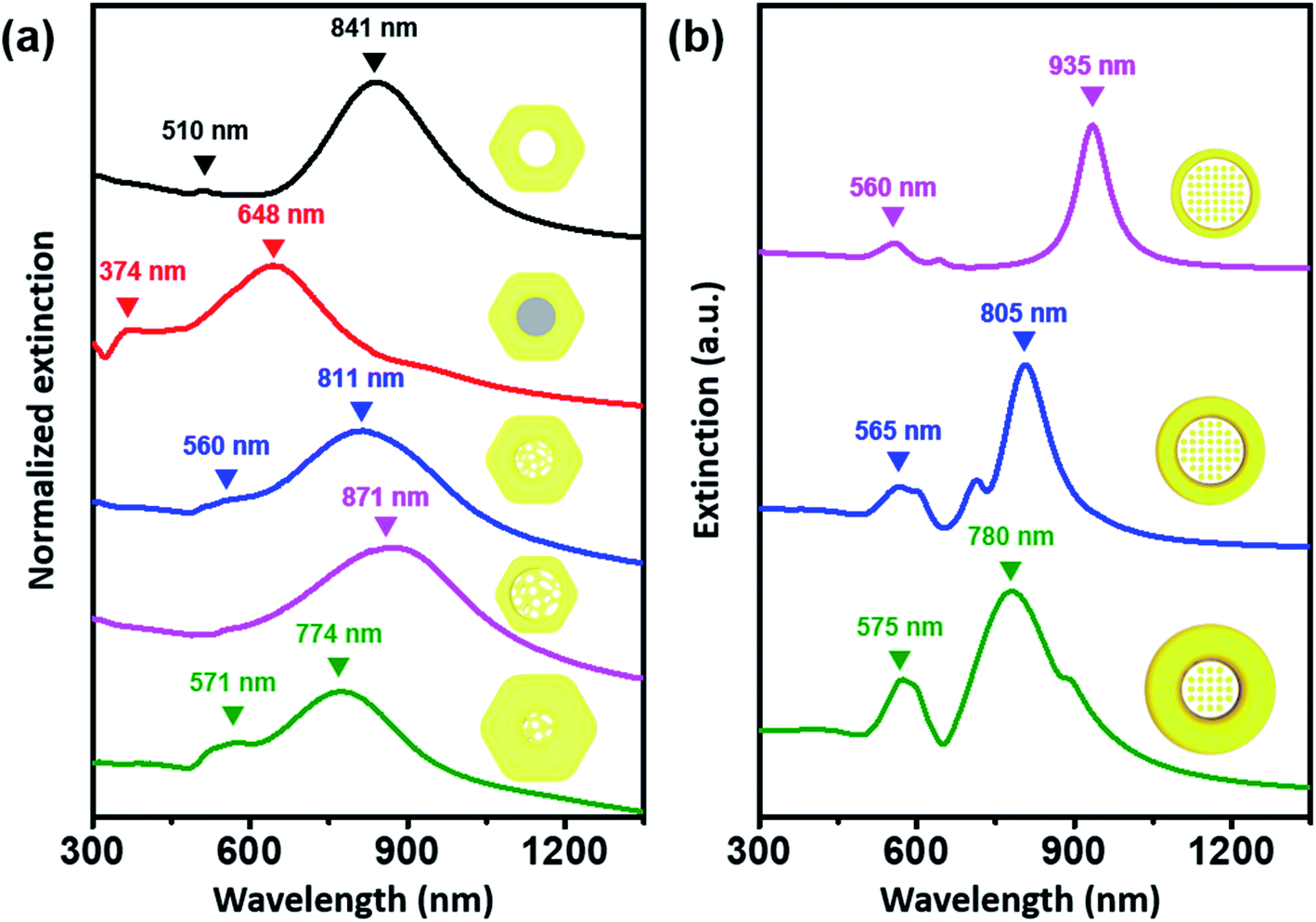 | ||
| Fig. 2 (a) UV-vis-NIR spectrum of Pt@Au nanorings (black line), Pt@Au@Ag nanodisks (red line), and Au nanolenses shown in Fig. 1d–f (pink, blue, and green, respectively). (b) Simulated extinction cross-section of Au nanolenses with variable inner and outer diameters. The detailed physical dimensions of the nanostructure model for theoretical calculation can be found in Fig. S5.† | ||
Theoretical calculations predicted the appearance of an in-plane dipole mode and out-of-plane dipole mode from the modeled structures (Fig. 2b, their physical dimensions are represented in Fig. S5†). We assumed the outer boundary of the modeled structure to be a circular shape instead of a hexagonal shape for convenience in the theoretical calculations. As the rim thickness of the Pt@Au nanorings increased, the in-plane dipole mode (bonding plasmonic mode) was blue-shifted, which correlated well with the experimental data. From the theoretical calculations, we could conclude that the LSPR characteristics of the Au nanolens structure were mainly affected by the plasmonic mode of outer light-absorber (Pt@Au nanorings), because the optical profile of the modeled nanostructure changed as a function of the physical dimension of the outer light-absorber. We could readily design the excitation wavelength of the nanostructures by tuning the physical dimension of the light absorber.
A schematic distribution of the electromagnetic near-field of the aforementioned Au nanolenses with respect to the electromagnetic polarization along the xy-plane was obtained via computer simulation (Fig. 3a). We performed electromagnetic simulations using the finite-element method (FEM) using COMSOL Multiphysics by adopting each physical dimension of the corresponding Au nanolenses. Nanolenses were modeled as a ring containing metal ligaments at the center. The diameters of the metal ligaments were 6 nm and the heights were the same as the thicknesses of each nanoring. All were arranged perpendicular to the xy-plane. The separation distance among the cylinders was fixed to 1 nm. As shown in Fig. 3a, the presence of a Au nanoporous structure at the center focused the near-field more effectively than Pt@Au nanorings with an empty hole (Fig. S6†). The central empty cavity of a Pt@Au nanoring is not effectively operative in terms of electromagnetic field focusing. However, Au nanolens with nanoporous network at the inner domain can effectively trap the electromagnetic field. Interestingly, the focused near-field exhibited the tendency of increasing field strength as the inner diameter decreased, which mimicked real-world converging lenses. As the rim size increased (concomitantly the central domain decreased), it absorbed more light and the central nanoporous structure accordingly focused the near-field more strongly. To experimentally demonstrate their near-field focusing capabilities, single particle SERS measurements were performed with dispersed Au nanolenses on glass substrates (thickness ∼0.13 mm) while monitoring them using Rayleigh scattering images. After single-particle SERS measurements, we obtained FE-SEM images of the same samples to confirm that we observed signals from a single nanoparticle (Fig. S7 and S8†). It was noteworthy that we found no deformation in the structure prior to and after SERS measurements, indicating the structural rigidity that was endowed by the inner Pt skeleton. For comparison, we obtained single-particle SERS (under 785 nm laser (170 μW)) of Au nanorings with and without the central nanoporous structure by varying their size (Fig. 3b). Among the investigated samples, there were no spectroscopic features from the Pt@Au nanorings (three samples from the bottom in panel b), showing their weak near-field focusing capabilities regardless of size. By contrast, Au nanolenses exhibited well-resolved SERS signals (three samples from the top), which indicated the capability for near-field focusing with the aid of a central porous structure. As predicted from the computer simulation, the signal-to-noise ratio of the observed bands systematically increased from 16.2 to 34.4 and 82.5 for Au nanolenses with inner diameters of 58 nm to 48 nm, and 35 nm, respectively.
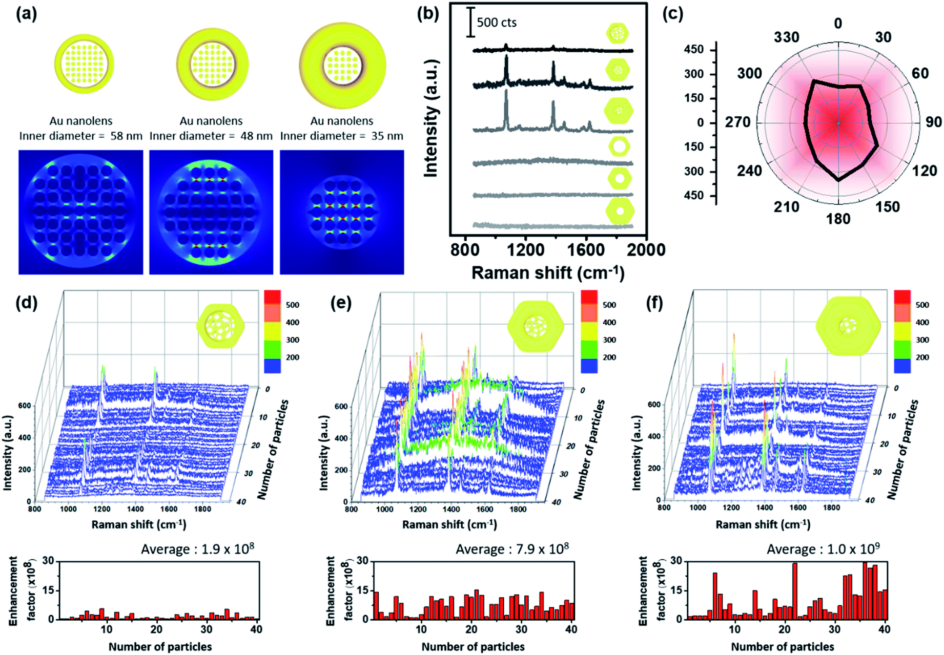 | ||
| Fig. 3 (a) Electric field enhancement contour maps of Au nanolenses varying by inner diameter. (b) Representative single-particle SERS spectra of Pt@Au nanorings and Au nanolenses with varying inner diameters. (c) Single-particle SERS intensity (at 1069 cm−1) of Au nanolenses as a function of polarization direction from 0° to 330°. (d–f) Single-particle SERS spectra plot of Au nanolenses with an inner diameter of 58, 48, and 35 nm, respectively. | ||
One noticeable feature was their signal independence on the polarization of incident laser light. Au nanolenses exhibited consistent SERS signal regardless of incident light polarization changing from 0° to 330°, which was attributed to the symmetric geometry of an Au nanolens “hot zone” (Fig. 3c, we plotted the original spectra in Fig. S9†). Usually, nanoparticle hot-spots were built by arranging two or more individual nanoparticles in a linear fashion. Then, the inter-particle junction played the role of focusing the near-field for SERS. With this configuration, it was a common observation that the SERS signals appeared only when the polarization was parallel to the long axis of the dimers, which limited the maximum utilization of incident laser light. Au nanolenses focused the near-field at the center with a symmetric geometry and could therefore be operative regardless of the polarization orientation, indicating the full-utilization of incident light energy for the SERS measurement. To evaluate the uniformity and reproducibility of the Au nanolenses as a single-particle SERS substrate, we acquired single-particle SERS of 40 individual nanoparticles for each sample and plotted them in Fig. 3d–f. The reproducibility and uniformity in the enhancement was poor with nanolenses possessing larger inner diameters (ca. 58 nm panel d). When the rim thickness increased to 43 nm and the inner diameter decreased accordingly to 48 nm, the measured SERS signals showed a strong enhancement and the corresponding enhancement factors are plotted below, ranging from 1.2 × 10⁸ to 1.6 × 10⁹, representing their narrow distribution. Furthermore, the observed enhancement factor of Au nanolens in this report is higher than the previously reported value with Ag double nanorings.19 Interestingly, when the rim size further increased to 56 nm (and the inner domain concomitantly decreased down to 35 nm), their enhancement further increased but exhibited a broad distribution in the enhancement factors ranging from 1.8 × 10⁸ to 2.9 × 10⁹. Once we found the Au nanolens with a “turned-on” status, the measured enhancement was stronger than the case of sample panel (d); however, the sample-by-sample reproducibility was not as good as the other case. From the detailed FE-SEM analysis, we found that the placement of Au nanolenses with thick rims was not flat on the substrate but instead stood up with a varied tilt angle. Therefore, the “turn-on” of the inner nanoporous structure was not as effective as the other cases with a flat orientation on the substrate (Fig. S11†). The inter-twined morphology of the inner nanoporous structure was quite stable under the given laser excitation and they maintained their “turn-on” state during the measurement.
Conclusion
In conclusion, we synthesized Au nanorings with a central Au nanoporous structure through an on-demand procedure, yielding near-field focusing ability and enabling the observation of single-particle surface enhanced Raman scattering. Pt@Au nanorings absorb light and the absorbed light can be focused onto the central Au nanoporous structure. By controlling electrochemical potential-tuned growth and the local surface energy of nanorings, we easily controlled the Ag growth pattern on Au nanorings. Then, the central nanoporous architecture was fabricated through a Galvanic exchange reaction. By varying the physical dimensions of the starting Pt@Au nanorings, we successfully tuned the inner diameter of the nanolens structure, leading to focusing of the electromagnetic field and allowing for reproducible and light-polarization independent measurements of single-particle SERS. Given that the Au nanolens SERS platform is highly optically active within the near-infrared range (785 nm) and is mainly composed of elemental Au (Au is inert to highly corrosive biological environments), we could apply this nanostructure toward biological applications.Author contributions
S. L., S. L., and J. M. K. performed the experiments and data analysis. S. P. and S. L. wrote the paper. J. S. and J. M. N. simulated FDTD method for electromagnetic field enhancement. E. C., S. Y., and H. H. contributed to interpretation of data.Conflicts of interest
There are no conflicts to declare.Acknowledgements
This research was supported by the Basic Science Research Program through the National Research Foundation of Korea (NRF) funded by the Ministry of Science, ICT & Future Planning (NRF-2017R1A2B3002796), the National Research Foundation of Korea (NRF) grant funded by the Korean government (MSIT) (NRF-2017R1A5A1015365), and the BioNano Health-Guard Research Center funded by the Ministry of Science and ICT (MSIT) of Korea as Global Frontier Project (H-GUARD_2013M3A6B2078947).References
- C. L. Haynes, A. D. McFarland and R. P. Van Duyne, Anal. Chem., 2005, 77, 338a–346a CrossRef CAS.
- S. Schlucker, Angew. Chem., Int. Ed., 2014, 53, 4756–4795 CrossRef PubMed.
- S. M. Nie and S. R. Emery, Science, 1997, 275, 1102–1106 CrossRef CAS PubMed.
- Y. W. C. Cao, R. C. Jin and C. A. Mirkin, Science, 2002, 297, 1536–1540 CrossRef CAS PubMed.
- D. Graham, D. G. Thompson, W. E. Smith and K. Faulds, Nat. Nanotechnol., 2008, 3, 548–551 CrossRef CAS PubMed.
- X. M. Qian, X. H. Peng, D. O. Ansari, Q. Yin-Goen, G. Z. Chen, D. M. Shin, L. Yang, A. N. Young, M. D. Wang and S. M. Nie, Nat. Biotechnol., 2008, 26, 83–90 CrossRef CAS PubMed.
- J. F. Li, Y. F. Huang, Y. Ding, Z. L. Yang, S. B. Li, X. S. Zhou, F. R. Fan, W. Zhang, Z. Y. Zhou, D. Y. Wu, B. Ren, Z. L. Wang and Z. Q. Tian, Nature, 2010, 464, 392–395 CrossRef CAS PubMed.
- W. Y. Li, P. H. C. Camargo, X. M. Lu and Y. N. Xia, Nano Lett., 2009, 9, 485–490 CrossRef CAS PubMed.
- D. Z. Chen, X. D. Zhu, J. Huang, G. Wang, Y. Zhao, F. Chen, J. Wei, Z. X. Song and Y. X. Zhao, Anal. Chem., 2018, 90, 9048–9054 CrossRef CAS PubMed.
- W. Q. Zhang, J. Liu, W. X. Niu, H. Yan, X. M. Lu and B. Liu, ACS Appl. Mater. Interfaces, 2018, 10, 14850–14856 CrossRef CAS PubMed.
- L. D. Qin, S. L. Zou, C. Xue, A. Atkinson, G. C. Schatz and C. A. Mirkin, Proc. Natl. Acad. Sci. U. S. A., 2006, 103, 13300–13303 CrossRef CAS PubMed.
- K. D. Alexander, K. Skinner, S. P. Zhang, H. Wei and R. Lopez, Nano Lett., 2010, 10, 4488–4493 CrossRef CAS PubMed.
- Q. Zhang, J. P. Ge, J. Goebl, Y. X. Hu, Y. G. Sun and Y. D. Yin, Adv. Mater., 2010, 22, 1905–1909 CrossRef CAS PubMed.
- V. T. Cong, E. O. Ganbold, J. K. Saha, J. Jang, J. Min, J. Choo, S. Kim, N. W. Song, S. J. Son, S. B. Lee and S. W. Joo, J. Am. Chem. Soc., 2014, 136, 3833–3841 CrossRef CAS PubMed.
- M. Yang, R. Alvarez-Puebla, H. S. Kim, P. Aldeanueva-Potel, L. M. Liz-Marzan and N. A. Kotov, Nano Lett., 2010, 10, 4013–4019 CrossRef CAS PubMed.
- D. K. Lim, K. S. Jeon, J. H. Hwang, H. Kim, S. Kwon, Y. D. Suh and J. M. Nam, Nat. Nanotechnol., 2011, 6, 452–460 CrossRef CAS PubMed.
- J. B. Song, B. Duan, C. X. Wang, J. J. Zhou, L. Pu, Z. Fang, P. Wang, T. T. Lim and H. W. Duan, J. Am. Chem. Soc., 2014, 136, 6838–6841 CrossRef CAS PubMed.
- J. Kim, S. Yoo, J. M. Kim, S. Choi, J. Kim, S. J. Park, D. Park, J. M. Nam and S. Park, Nano Lett., 2020, 20, 4362–4369 CrossRef CAS PubMed.
- S. Yoo, J. Lee, J. Kim, J. M. Kim, M. Haddadnezhad, S. Lee, S. Choi, D. Park, J. M. Nam and S. Park, J. Am. Chem. Soc., 2020, 142, 12341–12348 CrossRef CAS PubMed.
- M. Haddadnezhad, S. Yoo, J. Kim, J. M. Kim, J. Son, H. S. Jeong, D. Park, J. M. Nam and S. Park, Nano Lett., 2020, 20, 7774–7782 CrossRef CAS PubMed.
- S. Yoo, J. Kim, J. M. Kim, J. Son, S. Lee, H. Hilal, M. Haddadnezhad, J. M. Nam and S. Park, J. Am. Chem. Soc., 2020, 142, 15412–15419 CrossRef CAS PubMed.
- L. Rodriguez-Lorenzo, R. A. Alvarez-Puebla, I. Pastoriza-Santos, S. Mazzucco, O. Stephan, M. Kociak, L. M. Liz-Marzan and F. J. G. de Abajo, J. Am. Chem. Soc., 2009, 131, 4616–4618 CrossRef CAS PubMed.
- J. X. Fang, S. Y. Du, S. Lebedkin, Z. Y. Li, R. Kruk, M. Kappes and H. Hahn, Nano Lett., 2010, 10, 5006–5013 CrossRef CAS PubMed.
- Z. Liu, Z. B. Yang, B. Peng, C. Cao, C. Zhang, H. J. You, Q. H. Xiong, Z. Y. Li and J. X. Fang, Adv. Mater., 2014, 26, 2431–2439 CrossRef CAS PubMed.
- H. Wang and N. J. Halas, Adv. Mater., 2008, 20, 820–825 CrossRef CAS.
- H. J. You, Y. T. Ji, L. Wang, S. C. Yang, Z. M. Yang, J. X. Fang, X. P. Song and B. J. Ding, J. Mater. Chem., 2012, 22, 1998–2006 RSC.
- D. K. Lim, K. S. Jeon, H. M. Kim, J. M. Nam and Y. D. Suh, Nat. Mater., 2010, 9, 60–67 CrossRef CAS PubMed.
- B. Zhao, J. L. Shen, S. X. Chen, D. F. Wang, F. Li, S. Mathur, S. P. Song and C. H. Fan, Chem. Sci., 2014, 5, 4460–4466 RSC.
- M. Kim, S. M. Ko, J. M. Kim, J. Son, C. Lee, W. K. Rhim and J. M. Nam, ACS Cent. Sci., 2018, 4, 277–287 CrossRef CAS PubMed.
- J. W. Oh, D. K. Lim, G. H. Kim, Y. D. Suh and J. M. Nam, J. Am. Chem. Soc., 2014, 136, 14052–14059 CrossRef CAS PubMed.
- T. Jiang, G. Chen, X. L. Tian, S. W. Tang, J. Zhou, Y. H. Feng and H. Y. Chen, J. Am. Chem. Soc., 2018, 140, 15560–15563 CrossRef CAS PubMed.
- K. Liu, Y. C. Bai, L. Zhang, Z. B. Yang, Q. K. Fan, H. Q. Zheng, Y. D. Yin and C. B. Gao, Nano Lett., 2016, 16, 3675–3681 CrossRef CAS PubMed.
- S. Jeong, M. W. Kim, Y. R. Jo, N. Y. Kim, D. Kang, S. Y. Lee, S. Y. Yim, B. J. Kim and J. H. Kim, ACS Appl. Mater. Interfaces, 2019, 11, 44458–44465 CrossRef CAS PubMed.
- S. O. Kucheyev, J. R. Hayes, J. Biener, T. Huser, C. E. Talley and A. V. Hamza, Appl. Phys. Lett., 2006, 89 Search PubMed.
- T. Fujita, P. F. Guan, K. McKenna, X. Y. Lang, A. Hirata, L. Zhang, T. Tokunaga, S. Arai, Y. Yamamoto, N. Tanaka, Y. Ishikawa, N. Asao, Y. Yamamoto, J. Erlebacher and M. W. Chen, Nat. Mater., 2012, 11, 775–780 CrossRef CAS PubMed.
- M. J. Lee, S. H. Lim, J. M. Ha and S. M. Choi, Langmuir, 2016, 32, 5937–5945 CrossRef CAS PubMed.
- H. J. Jang, S. Ham, J. A. I. Acapulco, Y. Song, S. Hong, K. L. Shuford and S. Park, J. Am. Chem. Soc., 2014, 136, 17674–17680 CrossRef CAS PubMed.
- E. M. Larsson, J. Alegret, M. Kall and D. S. Sutherland, Nano Lett., 2007, 7, 1256–1263 CrossRef CAS PubMed.
- H. J. Jang, S. Hong, S. Ham, K. L. Shuford and S. Park, Nanoscale, 2014, 6, 7339–7345 RSC.
- S. Yoo, J. Kim, S. Choi, D. Park and S. Park, Nat. Commun., 2019, 10, 1–8 CrossRef CAS PubMed.
- G. S. Metraux, Y. C. Cao, R. C. Jin and C. A. Mirkin, Nano Lett., 2003, 3, 519–522 CrossRef CAS.
- L. M. Moreau, C. A. Schurman, S. Kewalramani, M. M. Shahjamali, C. A. Mirkin and M. J. Bedzyk, J. Am. Chem. Soc., 2017, 139, 12291–12298 CrossRef CAS.
- E. Prodan, C. Radloff, N. J. Halas and P. Nordlander, Science, 2003, 302, 419–422 CrossRef CAS PubMed.
Footnotes |
| † Electronic supplementary information (ESI) available. See DOI: 10.1039/d1sc00202c |
| ‡ These authors contributed equally to this work. |
| This journal is © The Royal Society of Chemistry 2021 |