
 Open Access Article
 This Open Access Article is licensed under a Creative Commons Attribution-Non Commercial 3.0 Unported Licence
Deep neural network analysis of nanoparticle ordering to identify defects in layered carbon materials†
Daniil A.
Boiko
 ,
Evgeniy O.
Pentsak
,
Vera A.
Cherepanova
,
Evgeniy G.
Gordeev
and
Valentine P.
Ananikov
*
,
Evgeniy O.
Pentsak
,
Vera A.
Cherepanova
,
Evgeniy G.
Gordeev
and
Valentine P.
Ananikov
*
Zelinsky Institute of Organic Chemistry, Russian Academy of Sciences, Leninsky Pr. 47, Moscow 119991, Russia. E-mail: val@ioc.ac.ru
First published on 29th April 2021
Abstract
Smoothness/defectiveness of the carbon material surface is a key issue for many applications, spanning from electronics to reinforced materials, adsorbents and catalysis. Several surface defects cannot be observed with conventional analytic techniques, thus requiring the development of a new imaging approach. Here, we evaluate a convenient method for mapping such “hidden” defects on the surface of carbon materials using 1–5 nm metal nanoparticles as markers. A direct relationship between the presence of defects and the ordering of nanoparticles was studied experimentally and modeled using quantum chemistry calculations and Monte Carlo simulations. An automated pipeline for analyzing microscopic images is described: the degree of smoothness of experimental images was determined by a classification neural network, and then the images were searched for specific types of defects using a segmentation neural network. An informative set of features was generated from both networks: high-dimensional embeddings of image patches and statics of defect distribution.
Introduction
Layered materials are composed of 2D layers and may undergo hierarchical organization into a variety of 3D frameworks.1 Specific features of layered materials make intercalation of guest molecules possible, enabling researchers to tailor the properties of the material.2 As one of the examples of layered material precursors, graphene has gained much attention, as it has unique physical properties: a wide electrochemical potential window, high capacity and carrier mobility, high stiffness and thermal conductivity.3–5 The properties of the material can be easily tailored by doping or further functionalization. Due to these features, graphene- or doped-graphene-based materials have been used in the development of electronic devices,6 energy storage,7 catalysts,8–10 medicine,8,11 and physical,12 chemical,13,14 and biological15,16 sensors. Beyond graphene structures, several other layered materials have inspired a number of applications.Assessment of the surfaces of layered materials and revealing defect areas is a question of key importance since the performance of the materials strongly depends on the absence/presence of defects. High-quality defect-free surfaces are important for a number of industrial applications, such as electronics,1 LEDs,17 composites,18 and materials with high mechanical strength.19 (Fig. 1). In contrast, it could be supposed that materials with a large number of defects are practically useless, but certainly this is not the case. Materials with surface defects are highly important in other areas (Fig. 1). For example, defect engineering may help to develop sensors with remarkably high selectivity,20 defect construction in electrode materials plays a crucial role in electrochemical reactions,21 defect-abandoned charcoal materials are superior for water purification,22,23 and controlled surface defects govern the synthesis of industrially important catalysts.24,25 Thus, detection of the number of defects and classification of the type of defect is a highly important topic of paramount practical importance (see more details in the ESI†).
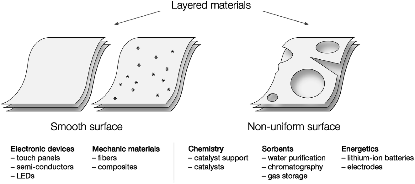 | ||
| Fig. 1 A few representative areas of application of different smooth materials and materials with defects. Stars represent uniformly distributed point defects. | ||
Some types of defects can be visualized by electron microscopy and traced in chemical transformations.26–29 However, the difficulty lies in obtaining sufficient microscopy contrast within a surface composed of the same elements. The challenge is that various types of defects are “hidden”, i.e. invisible with regular inspection by standard analytic tools. The defects may remain “invisible” until the material is used in a certain application, where a different chemical reactivity of defect areas comes into play (defect areas are usually much more chemically reactive than smooth areas).
For the analysis of complex patterns, deep learning has received more attention in a variety of chemical applications, from the analysis of materials and objects present in the chemical lab30 to the discovery of receptor inhibitors.31 The application of machine learning for the analysis of microscopy images is a high priority area for nanoscience. As a few representative examples, the application of machine learning in scanning electron microscopy (SEM) imaging involved the creation of the SEM image dataset,32 which was then analyzed using convolutional neural networks.32 Machine learning was used in transmission electron microscopy (TEM) for particle recognition and tracking.33 An in-depth study was performed for particle segmentation.34 In optical spectroscopy, a neural network-based algorithm was used to autonomously search for 2D materials.35 Nanoparticle recognition was accelerated in scanning probe microscopy.36
In the present study, we utilized the concept for visualization of defects using metal nanoparticles as contrast agents, and we developed a machine learning approach for automated analysis of both parameters—the number and type of defects. Two machine learning tasks were solved, and the corresponding results and algorithms were analyzed, yielding unique features for the quality assessment of layered carbon materials.
Results and discussion
Description of a concept
A general approach utilized in the present study is shown in Fig. 2. A possible solution to visualize “hidden” defects is to attach metal nanoparticles to the surface of the material. Due to the higher chemical reactivity of defect areas, they can be efficiently visualized using metal nanoparticles as contrast agents in spatial imaging.37,38 Smooth surfaces should demonstrate a random location of metal nanoparticles since there are no preferential binding sites.39 Theoretical modeling with DFT calculations has shown that moderate binding energy should be expected for metal attachment to nondefective graphene surfaces.37,40 The binding energy considerably increases upon the appearance of defect areas.37,40 As an estimate, on grain boundaries the affinity to palladium is 31% higher than on pristine graphene; for Stone–Wales defects, this effect is even more pronounced with 42% higher affinity.37,40 Indeed, if defect sites are present on the surface, they will predominantly capture metal atoms and result in the formation of patterns that reflect the geometry of a particular defect area. Direct association between particle attachment and underlying defect sites was confirmed by experimental methods.37,39,41,42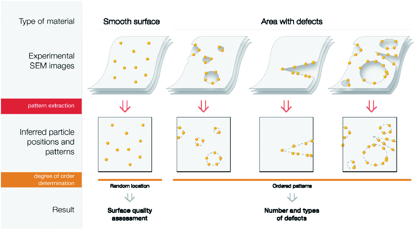 | ||
| Fig. 2 Usage of nanoparticle ordering to analyze the quality of the surface and number of defects. | ||
Thus, the appearance of ordered patterns on the surface of a material may serve as an indication of the presence of defect areas. Moreover, nanoparticles highlight chemically reactive areas, which cannot be done by direct imaging without contrast agents. The visual arrangement of metal particles underlines the topography of the defect area (Fig. 2). Particularly, using electron microscopy, a number of different defects, such as sheet borders, grain boundaries, sheet bends, and point defects, may be visualized on the marked carbon surface. The experimental procedure for nanoparticle attachment to the carbon surface is simple and straightforward. Subsequent electron microscopy analysis generates a large number of images suitable for automated analysis. Decoration by nanoparticles has been successfully demonstrated for various materials.43–47 Recently, an electron microscopy dataset with a thousand images was created to visualize defect areas marked with metal nanoparticles.48
Experimental procedure using a solution of a simple palladium complex as a contrast agent
The experimental design involves the generation of palladium nanoparticles from the molecular complex Pd2dba3 (dba = dibenzylideneacetone) in situ with a carbon material present in the reaction mixture. Therefore, when the particles are deposited, the pattern of their positions will closely resemble the electronic properties of the surface. The experimental procedure applied here was previously proven to generate a large dataset of images with nanoparticle ordering patterns.48 The procedure included heating the mixture of easily available metal complex Pd2dba3 and carbon material in CHCl3 at 80 °C in a screw-capped tube for 1–5 minutes. During heating, the complex is decomposed, leading to the disappearance of the pink color of the solution. As a result, palladium is deposited on the material, and only free dba ligand is left in the solution. The size of the metal nanoparticles was in the range of 1–5 nm, which is perfectly suitable for accurate detection with electron microscopy.Then, the material with deposited nanoparticles was filtered off and subjected to SEM analysis. To illustrate the difference, two carbon materials with and without ordered defects on the surface were analyzed, and a clear difference in the degree of palladium nanoparticle ordering was observed (Fig. 3). Nanoparticle ordering marked the underlying surface defects.
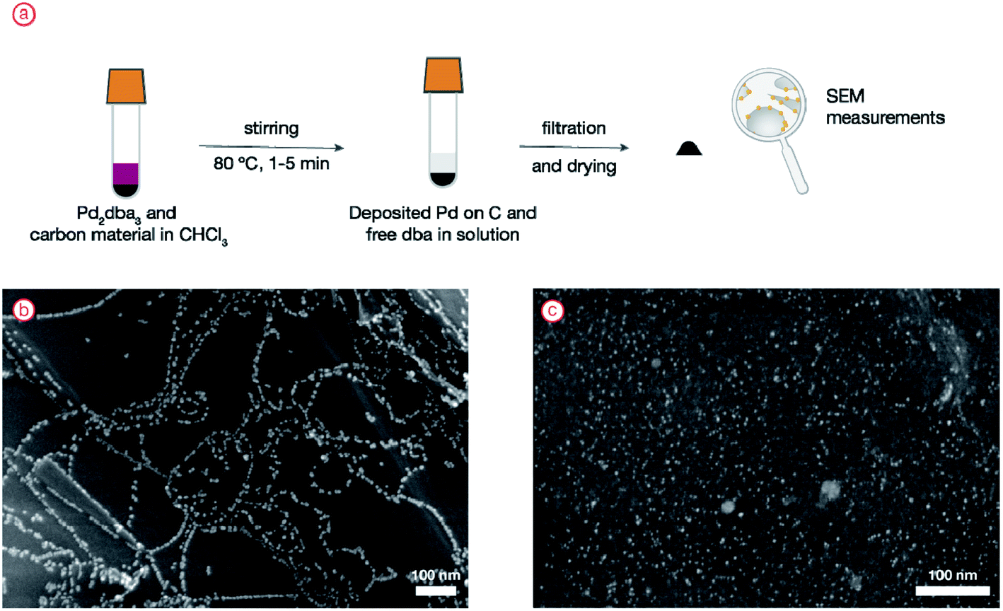 | ||
| Fig. 3 (a) General scheme of the experiment; (b) experimental image showing ordered nanoparticle location; (c) experimental image showing random nanoparticle location. | ||
This experiment was performed to test the reproducibility and to analyze real experimental microscopy images in the present study. A general applicability of this approach was confirmed for a number of systems.37,49–51 In the present article, we also performed an analysis of microscopy images published previously.48
Ordering of nanoparticles is caused by the presence of defect areas: proof of concept with computational modeling
To confirm the direct relationship between the observed ordered structures and underlying surface defects, we performed Monte Carlo simulations of the nanoparticle deposition process. The model includes three actions of particles: adsorption of the particles from the solution, leaching of the particles back into the solution, and on-surface movement of the particles.These three particle movement pathways are well known and described in the literature.52 Adsorption is crucial for the deposition of nanoparticles onto the carbon material surface. Binding energies between palladium clusters and carbon material surfaces were previously calculated37 and show large (tens of kcal mol−1) differences between moderate binding to pristine surfaces and strong binding to defects such as sheet borders, grain boundaries, and Stone–Wales defects. The reverse process—nanoparticle leaching—was also studied as a part of the redeposition process of Pd nanoparticles.53 Concerning on-surface nanoparticle movement, Pd atoms are known54 to be able to move on the graphene surface until they face a defect area, where their movement stops.
To substantiate the correctness of the assumptions used for the simulation by the Monte Carlo method in this work, we performed molecular modeling of the adsorption of palladium clusters on the graphite surface using the GFN2-XTB quantum chemical method, which is based on the DFT approach. The molecular model consisted of a sheet of graphene C262 and a Pd13 cluster. Since the area of a defect-free carbon material is much larger than the area of defects, at the first stage, the cluster is most likely adsorbed on the defect-free graphite surface. Binding of the cluster to the carbon surface occurs due to the coordination of one of the Pd3 flat faces of the icosahedron with the C2 and C3 groups of carbon atoms. The energy of this process at this level of theory is −91.9 kcal mol−1; that is, simple desorption of the cluster from the graphite surface is unlikely. However, the migration of a cluster over a defect-free graphite surface apparently occurs without significant energy changes. In particular, the gradual displacement of the cluster from the center to one of the edges as a result of relaxed scan calculation leads to insignificant fluctuations in the total energy of the system: the maximum increase in the total energy did not exceed 5.0 kcal mol−1. Therefore, the activation energy of this process may be approximately in the same range.
To further confirm the possibility of low-energy cluster migration over a defect-free graphite surface, we performed a molecular dynamics (MD) simulation of the Pd13·C262 system by the GFN2-XTB method at a temperature of 350 K, which corresponds to the temperature of palladium nanoparticle formation on the graphite surface in the experiment. The initial state for MD simulation was the optimized structure of the Pd13·C262 complex, in which the cluster was adsorbed at the center of the carbon material surface. As a result of MD simulation, the cluster gradually moved to one of the edges of the carbon sheet in approximately 7 ps. The mechanism of migration of this cluster is an alternation of “sliding” and “rolling” of the particle over the graphite surface. In both cases, the energy consumption for the dissociation of one of the Pd–C bonds is immediately compensated by the energy gain due to the formation of a new Pd–C bond; as a result, the total energy change during cluster migration turns out to be rather small (close to zero).
A significant exothermic effect is achieved when the cluster is bound to the unsaturated edges of the graphite surface. For example, the adsorption energy of a cluster at the armchair edge is −191.0 kcal mol−1, while the adsorption energy at the zigzag edge is −248.9 kcal mol−1. In both cases, the cluster is bonded to edge carbon atoms by five palladium atoms. Thus, the energy profile of the process of interaction of palladium clusters with a graphite surface, which is the basis for the Monte Carlo simulation, is fully confirmed by the quantum chemistry method.
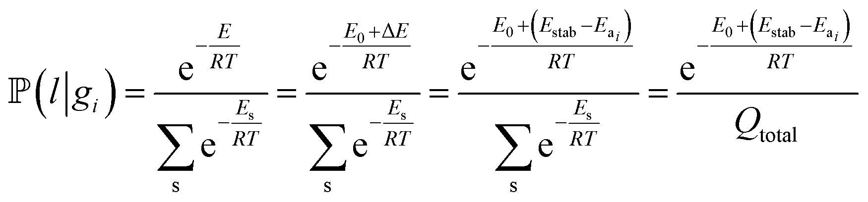
To perform the simulation, probabilities were chosen in a way (Fig. 4) in which they qualitatively agree with the energy surface but also allow us to observe the dynamics of the process (see details in the “Methods” section). In the general model, for each type of carbon material surface gi, we have conditional probabilities 
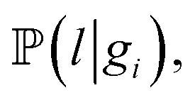 and
and 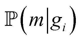 for adsorption onto defect gi and leaching and movement for particles located on gi, respectively. The conditional probability
 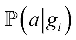 was decomposed via the chain rule:
 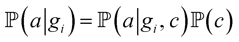 , where event c represents a close approach of a nanoparticle to the carbon material surface.
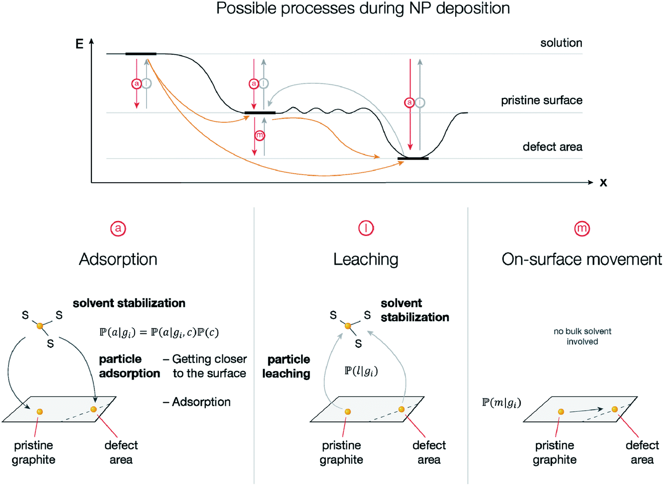 | ||
| Fig. 4 Top – schematic energy diagram reflecting the model of nanoparticle attachment to the surface; bottom – particle movement pathways: adsorption, leaching, and on-surface movement. The ripple pattern represents irregularities of electron density on the surface. Light gray arrows represent processes with low probability. | ||
In the quasi-equilibrium assumption, the probabilities of finding the particle on a specific type of surface or in the solution can be estimated using a Boltzmann distribution. For example, in the particle leaching case we have:
To run the simulation, a number of particles (initially all of them are in the solution) were generated, and then iteratively, each type of movement was sampled and applied to each particle. The system converges at hundreds or thousands of iterations, and the exact number depends on the number of particles (Fig. 5). Corresponding snapshots from representative simulation steps are presented as images in the ESI.† Dynamic surface changes during the simulations were captured by video, and the movies are available in the ESI.†
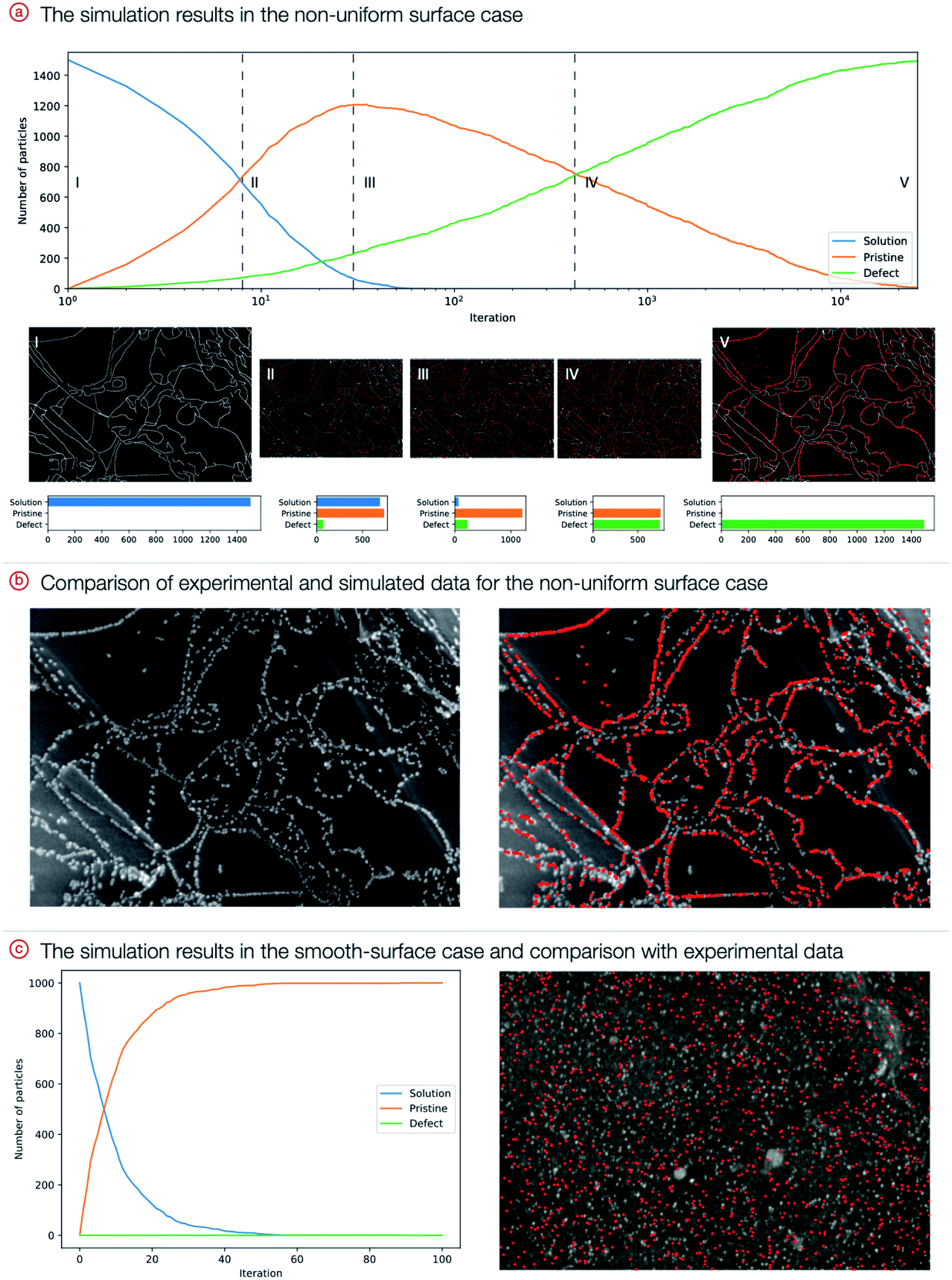 | ||
| Fig. 5 (a) The simulation results for a nonuniform surface case. The plot represents the amount of palladium (in particles) present in the solution, on the pristine surface, and on the defect surface. Images show the simulation state after a certain number of iterations. Histograms show the amount of palladium. (b) Initial experimental image and overlaid simulation results in the nonuniform surface case. (c) The simulation results in the smooth-surface case: a plot of the amount of palladium and overlaid final state. | ||
The results clearly indicate that the presence of defects is highly likely to be responsible for the formation of ordered patterns. Simulations show strong agreement with experimental data: the distribution of final nanoparticle locations closely resembles the actual distribution, and curves of palladium content in the solution and on the material are in agreement with the first-order kinetics of the experimental processes.37 For the disordered case, particle positions are different from experimental positions; this is caused by the inherent stochasticity of the deposition process onto smooth materials (random attachment) without distinct defect areas on the surface.
Machine learning algorithms are suitable for characterization of the degree of order
To analyze how the presence of defects impacts the properties of the materials, one will need a way to describe the ‘defectiveness’ of the material quantitatively. In the case of Pd nanoparticle imaging, this means measuring the degree of order of particle positions. It is important to note that uniformly distributed point defects will give a uniform distribution of single palladium nanoparticles. Therefore, ordered Pd-nanoparticle arrangements highlight linear defects (sheet borders, grain boundaries, topological defects), groups of point defects, pores in graphene layers, or graphene “islands”.The problem of determining the degree of order may be solved either by sequential decomposition of the problem or by developing an algorithm, which would give a degree of order directly from the image. The first approach would mean that the location of particles is needed, so then one could use distances between the observed distribution of particle positions and uniform distributions (statistical tests of that are well known58). Despite its strong mathematical grounding, this method has some disadvantages: first, in some cases, particles are out of focus in SEM images, so determination of their exact positions is difficult; second, depending on the topology of the material, the density of particle positions may change (see an example in the ESI†). Therefore, we chose a much more robust second option—to train the end-to-end pipeline, based on classification neural networks (Fig. 6).
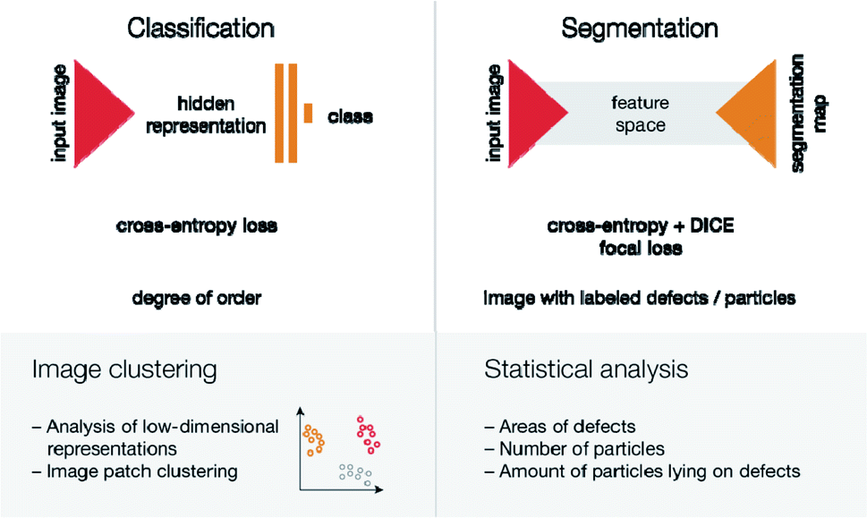 | ||
| Fig. 6 Two tasks for neural networks and ways for further analysis. From top to bottom: name of the task, network architecture scheme, loss function(s), the output of the network, possible ways for further analysis. The triangle represents the contracting/expanding path. Vertical rectangles represent fully connected layers. The gray shape between triangles represents a change to feature space and layer concatenation, as is done in U-Net.59 | ||
The neural network classifier outperforms humans in the image classification task
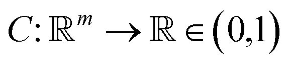
Any classification neural network essentially is a function that maps every image into the interval (0,1), where n is the side length for a square image. This number can be treated as a probability to belong to the corresponding class of the image.
Many neural network architectures have been developed to solve image classification problems. The modern state of the field began with the development of AlexNet, the winner of the 2012 ImageNet competition.60 Like many other architectures, it follows an encoder-fully connected classifier scheme.
We compared three popular neural networks: AlexNet,60 ResNet,61 VGG80-encoder-based networks. As classifiers return “probability”, depending on the threshold, one may obtain different accuracy, precision and recall scores. It is important to note that these “probabilities” may not be interpreted as real probabilities, especially in some modern neutral networks.62 Therefore, to maintain threshold invariance, classifiers are usually compared using the ROC AUC score (area under the receiver operating characteristic curve).
These networks were trained using cross-entropy loss. The learning was extremely fast: in many cases (except for the AlexNet network), the networks were able to provide ≥90% accuracy, and ≥0.95 ROC AUC score within only 100 epochs. The ResNet-based model outperforms AlexNet in all metrics, having fewer parameters (Table 1).
| Neural network | Number of parameters | Accuracy | Precision | Recall | ROC AUC score |
|---|---|---|---|---|---|
| a “All” means two groups of people who passed and did not pass the test. b Only those who passed the test (see the ESI for details). | |||||
| AlexNet | 57M | 0.80 (0.907) | 0.71 (0.907) | 1.00 (0.980) | 0.92 (0.943) |
| ResNet34 | 21M | 0.95 (0.979) | 0.91 (0.980) | 1.00 (0.993) | 0.98 (0.987) |
| VGG-13 | 129M | 0.95 (0.984) | 0.91 (0.987) | 1.0 (0.993) | 1.0 (0.995) |
| Human brain (all)a | Many | 0.869 | 0.943 | 0.796 | N/A |
| Human brain (passed the test)b | Many | 0.896 | 0.962 | 0.837 | N/A |
| Human brain (expert, one of the authors) | Many | 1.000 | 1.000 | 1.000 | N/A |
These results were compared with manual human labeling. 245 people were asked to look at some examples of ordered and disordered images and then to classify 25 images: first 5 images were used as a test—they contained very simple examples and let us exclude those results, where the problem was misunderstood (see all poll questions in the ESI†). Human results were good, but compared to the neural networks, people were much slower (few seconds vs. milliseconds), and the metrics were worse. This indeed confirms the importance of automated analysis in microscopy imaging.
Saliency map analysis shows that the network learned meaningful features
Then, we tried to shed light on what makes images look ordered for neural networks. As previously stated, a deep classifier maps images to some number S∈(0,1) (if a sigmoid function is used as activation). Therefore, the “influence” of each part of the image I0 on the classification score can be computed as the corresponding derivative:
It can be easily computed using standard backpropagation.63 The results may be improved by further operations using deconvolution or guided backpropagation methods.64
Even using standard backpropagation (Fig. 7), we see that empty areas of the carbon material surface have the greatest impact on the neural network's decisions. The image of the disordered class, in contrast, gives a strong response in only one ordered-looking part of the image. Therefore, we can consider that the neural network indeed learned some semantically relevant features.
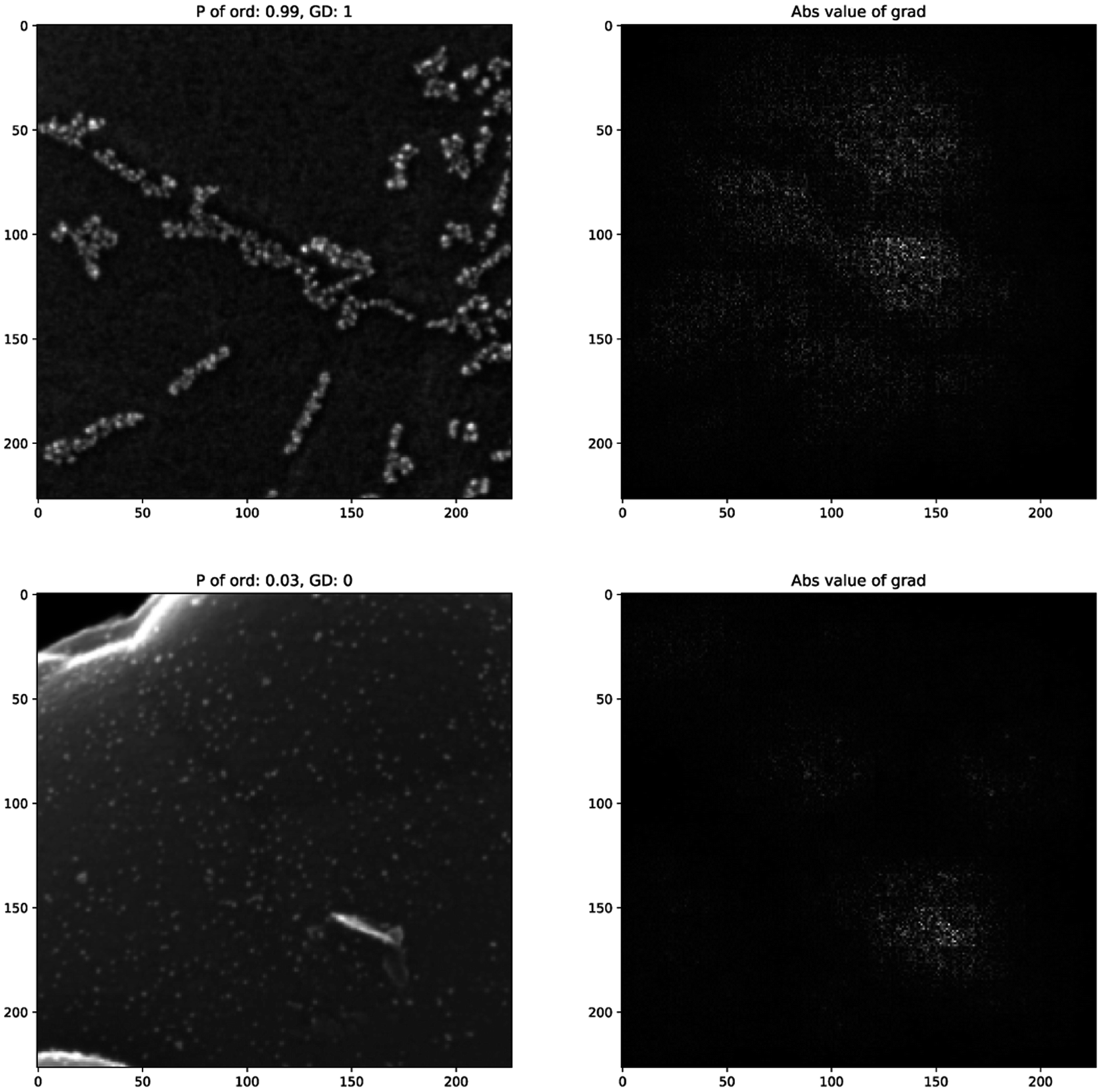 | ||
| Fig. 7 Examples of saliency maps (right) of correctly classified experimental images (left) of both classes. | ||
Learned image embeddings catch semantically meaningful information
The architecture of neural network classifiers NN usually contains two parts: encoder E—a network, which maps images into vectors of fixed length m, and a fully connected network C, which performs classification using these features.
| NN = C(E(I)) |
Therefore, during training, one is not only learning parameters of the classification network itself but also training an encoder, which is learned in that way, in which it keeps the most valuable information to perform the classification.
We show that these vector representations of images indeed reflect semantically meaningful information about the image: the position of the specific image patch in the feature space of the neural networks can tell a lot not only about the degree of order (two classes are separable even in two PCA coordinates) but also about the sample (Fig. 8). We see, for example, that sample S3 can be relatively easily separated from other images. Some of the samples overlap greatly, especially S1 and S3.
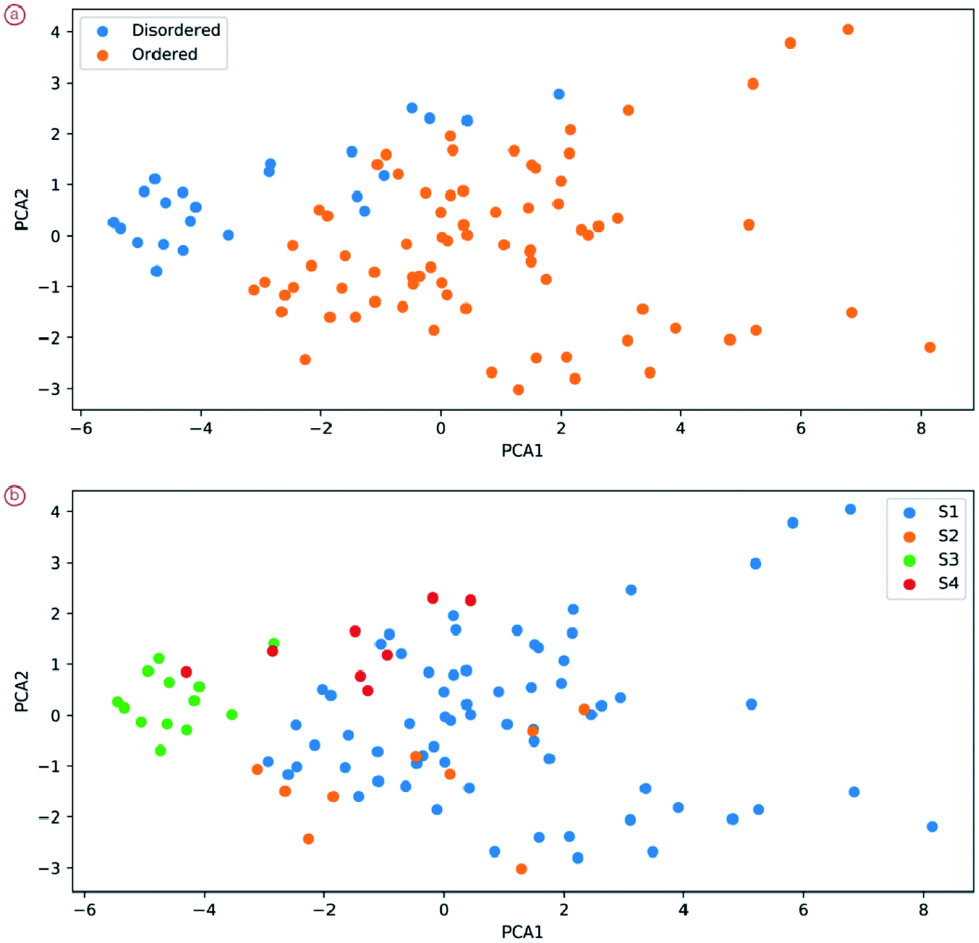 | ||
| Fig. 8 Positions of random patches from images of different degrees of order (a) and different samples (b). | ||
Training classifiers, we obtain feature vectors for other machine learning algorithms: we can put another model (gradient boosting, for instance) on top of the features and solve other machine learning tasks. Distances between embeddings for image patches of different materials can be applied to compare them.
In conclusion, it is shown that the degree of nanoparticle ordering can be easily identified using basic classification neural network architectures such as AlexNet. The networks indeed learn semantically relevant information and may give not only information about the degree of order but also information about the sample in general.
Learning can also be done on different types of defects
More features can be obtained not only by solving the classification problem but also by analyzing what type of defects cause irregularities in particle positions. Therefore, one needs to map one image (SEM microphotograph) into another multichannel image, where each channel corresponds to a specific type of defect. This requires learning a function (neural network in our case) where c is the number of classes. This type of problem is called image segmentation (Fig. 6).
For analysis we considered four types of defects:
(1) Sheet borders
Usually, they have sharp sheet borders with nanoparticles. The brightest part of the image if one is not overexposed.
(2) Grain boundaries
A curvy pattern of particle positions. Usually, it is not possible to detect using only background (without particles) images.
(3) Topological defects
Surface bends caused a soft gradient of brightness. Particles were located on concave defects, while fewer particles were usually observed on convex defects.
(4) Point defects
Local defects can bind groups of at least 5 agglomerated nanoparticles.
Sheet borders and topological defects can be observed even without Pd-NP markers, but grain boundaries and point defects cannot be observed by traditional SEM techniques.
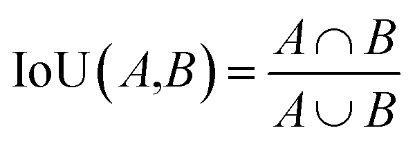
The training data were generated by labeling 15 images. Models were compared using the intersection over union (IoU) score on the validation dataset. This metric is defined as follows:
As the labels contain thin lines with very high variability in their positioning, the scores are not very high. For the best model—FPN with SE-ResNet50 encoder, 0.31 IoU score was obtained. However, as we see (Fig. 9), the model is absolutely suitable for the determination of defect statistics. Defects present on the material surface are correctly identified. Moreover, the high generalization ability of the model helped to find defect sites that were not labelled by the expert. This also lets us suggest that using pseudolabelling along with the entire dataset one may improve the model's accuracy.
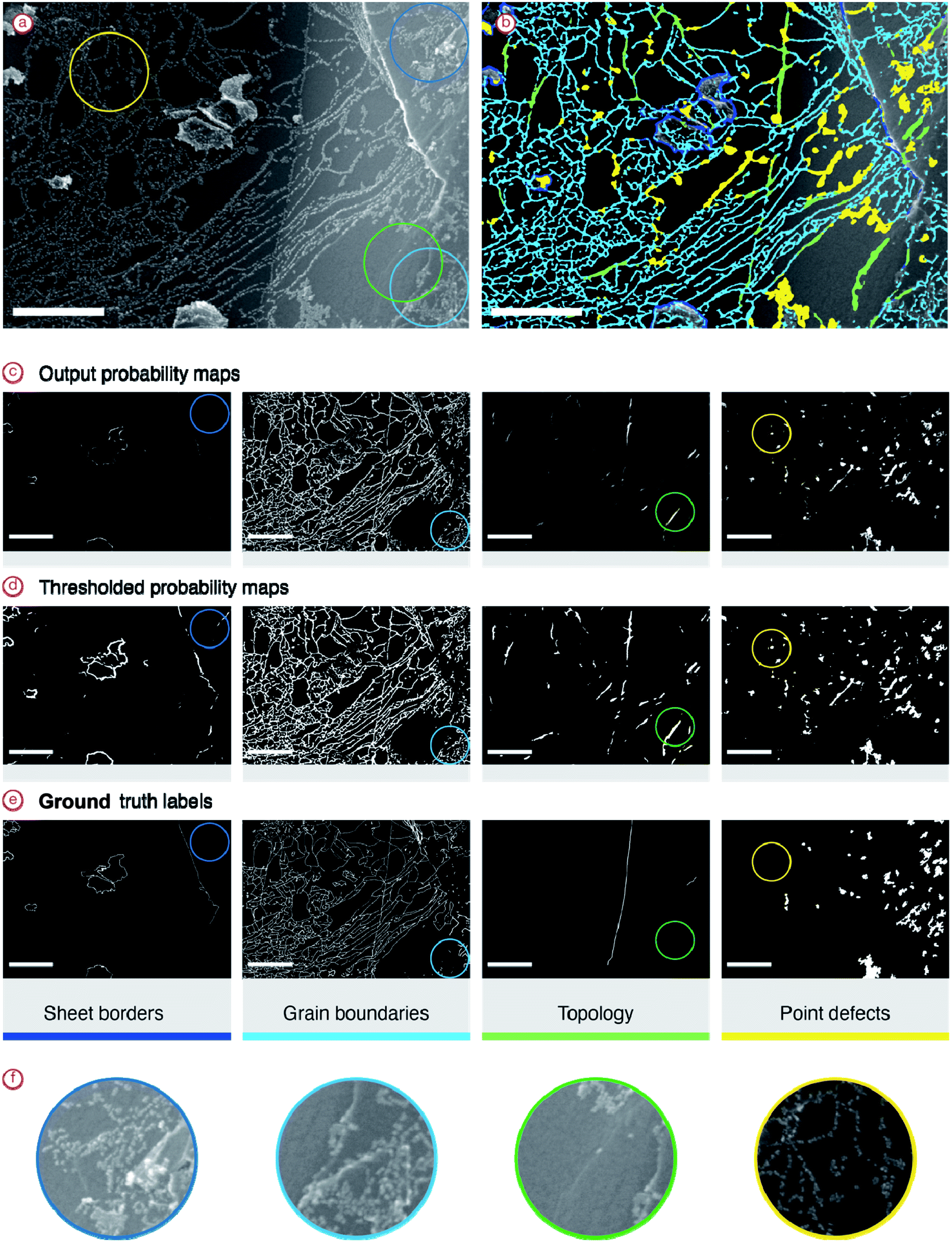 | ||
| Fig. 9 Example of automatically labeled images from the validation dataset: (a) experimental image, (b) experimental image with highlighted defect areas (overlaid thresholded neural network outputs), (c–e) normalized probability maps, thresholded probability maps and ground truth labels, (f) zoomed areas of the image where the network was managed to find defects, which are not present in the ground truth. | ||
Further analysis of line objects (sheet borders and grain boundaries) can be performed based on skeletonized images (Fig. 10). Skeletonization is a process of sequential dilation of the mask until lines become one pixel wide. Therefore, the number of pixels in the skeletonized image would give a good estimation of the length of the corresponding patterns. This also reduces the inherent noise of the neural network outputs.
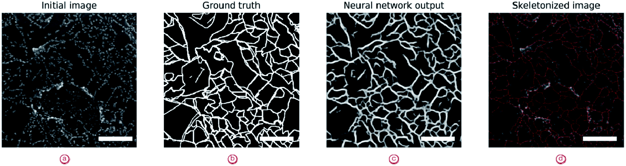 | ||
| Fig. 10 Skeletonization of segmentation maps. (a) Initial image, (b) ground truth with grain boundaries and sheet border combined, (c) neural network output, (d) result of skeletonization. Scale bar—200 nm. | ||
Thus, segmentation makes it possible to analyze the reasons for the nonuniform distribution of defects on the surface of the carbon materials. At the same time, segmentation was successfully performed for images of surfaces with complex morphology, as well as for images of mediocre quality. This was enabled by extensive augmentation of the images.
Conclusions
In this study, we developed an approach for analyzing the surface of a carbon material using a combination of Pd nanoparticle imaging and neural networks. Applying Monte Carlo simulations, it was shown that the effect of nanoparticle ordering is associated with defects on the material surface.Machine learning analysis of experimental images is presented in two tasks: classification and segmentation. By classifying images into ordered and disordered images, one can obtain a “probability” of being ordered, which can be used as a metric of uniformity, surface smoothness and the absence of extensive defects. It is shown that image embeddings from the encoding part of the network are semantically relevant. An analysis of learned features was also carried out. The trained networks showed superhuman performance.
Solving the segmentation problem, we additionally obtained more information about the types of defects, which caused irregularities of nanoparticle positions. Further ways of analysis are described: it was found that skeletonization operation is the crucial step for statistical analysis of linear defects.
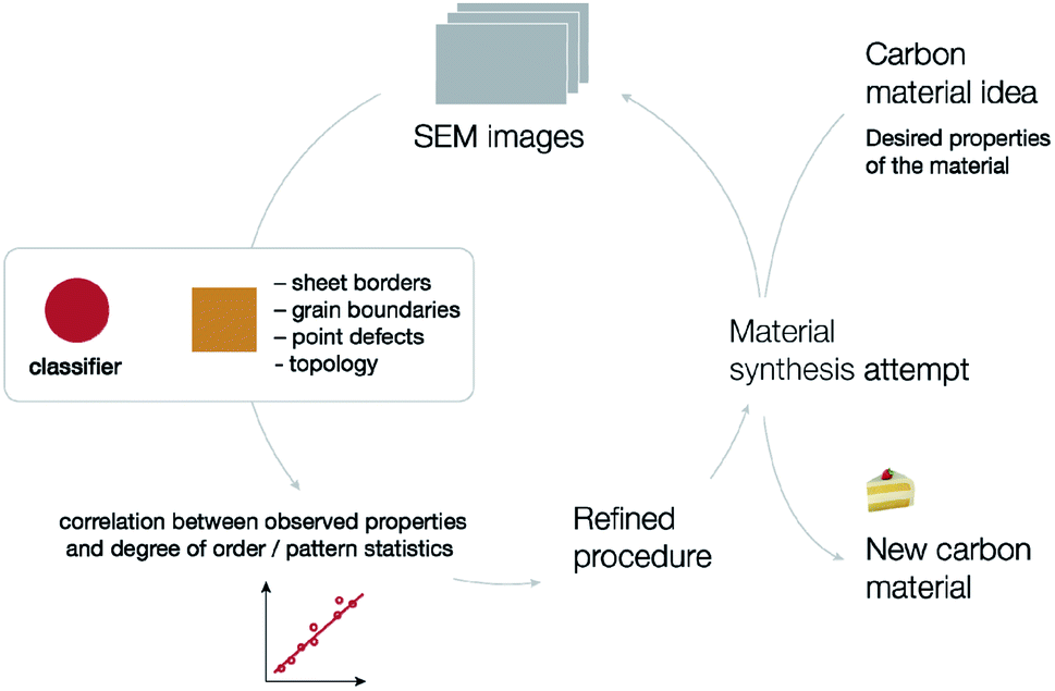
These results can be combined into a unified approach to material development (Fig. 11). To create a new material with desired properties, we propose imaging of the material followed by automated neural network analysis (this includes classification to get the degree of order and image patch embeddings and segmentation to identify specific types of defects and compute corresponding statistics), search for correlations between observed properties and neural network analysis results. The results of such machine learning analysis are indeed linked with the actual structure of the material. Knowing how the structure of a material impacts its properties, one can redesign the synthetic procedure and repeat the same process again. This procedure would be much less effective without automated analysis, as there would be no quantitative measure for structural changes.
 | ||
| Fig. 11 Summary of the proposed approach for material development, boosted by nanoparticle imaging and neural network processing. | ||
In this work, we test the described approach using carbon materials as an example. We expect that this approach can also be useful for a number of other layered materials, where defect regions can react with metal nanoparticles. Further research on this topic is underway in our laboratory.
Methods
Sample preparation
Pd2dba3·CHCl3 (5 mg), a carbon material (100 mg) and CHCl3 (5 mL) were mixed in a screw-cap tube. The reaction mixture was stirred at 80 °C for 5 minutes. The carbon material with deposited Pd was then separated, washed with acetone to remove dba and dried. The samples were then subjected to SEM study.Scanning electron microscopy
The samples were mounted on an aluminum specimen stub and fixed with conductive graphite adhesive tape. Then, they were studied using a Hitachi SU8000 field-emission scanning electron microscope (FE-SEM). The images were acquired in secondary electron mode at an accelerating voltage of 10–30 kV and a working distance of 6–12 mm.Computational details
All quantum chemical calculations were performed by the GFN2-XTB method using the XTB 6.4.0 software package.65–69 The GFN2-XTB method, like the DFTB methods, is based on density functional theory. DFTB methods include pairwise empirical parameterization, while GFNn-XTB methods include empirical parameterization for individual atoms, which is a crucial advantage of the latter over DFTB methods. The accuracy of the GFN2-XTB method is comparable to that of the DFTB methods and, in many cases, is comparable to the accuracy of the DFT methods. The empirical parameterization of the GFN2-XTB method includes all elements up to radon; thus, this method can be used to model molecular systems containing transition metal atoms, including metal clusters.70,71The edges of the graphene plane were unsaturated on all four sides and were models of the grain boundaries characteristic of the graphite and graphene planes.55–57 The palladium cluster is an icosahedral structure with one palladium atom in the center.
The Pd13 cluster, when coordinated with ligands, is prone to a transition to a low-spin electronic state.72 Taking into account this fact, as well as the features of the GFN2-XTB method, all molecular systems were calculated in the singlet electronic state. As shown earlier, different isomers of the Pd13 cluster differ from each other by no more than 1 eV.72 Since the adsorption energies are very significant and substantially exceed this difference, the analysis of various isomers of the Pd13 cluster by the GFN2-XTB method was not performed in this work.
To calculate the adsorption energy of the Pd13 cluster on the C262 surface, a total optimization of an isolated cluster, an isolated plane, and a Pd13·C262 complex was performed. The adsorption energy was calculated as:
| Eads = Ecomplex − Ecluster − Eplane |
When performing relaxed scan calculations, the scan coordinate was chosen as the distance between one of the palladium atoms of the cluster, which is directly bonded to the graphite plane, and one of the carbon atoms at the edge of the plane. At the initial scanning point, the cluster was adsorbed at the center of the carbon surface. In the course of scanning, the selected Pd–C distance decreased from 9.943 Å to 2.544 Å in 50 scanning steps, i.e. the step size (∼0.148 Å) was small enough so that when the cluster was moved at each step, there would be no cluster rearrangements.
Molecular dynamics simulations were performed at 350 K (NVT ensemble, Berendsen thermostat), and time steps were equal to 1.0 femtosecond. The analysis of the MD modeling results was carried out using the VMD software package.73
Monte Carlo simulations
Particle concentrations and probabilities were chosen to better represent experimental data and quantum chemistry calculations. The simulations started with 1500 particles in the ordered case and 1000 particles in the disordered case. Initial defect distribution maps were prepared by manual labelling of the corresponding experimental images.For each simulation step, each possible type of movement was applied to every particle. For the adsorption process, solution particles were moved randomly across the field and then adsorbed with 0.1 probability. For particles already positioned on the surface, leaching and surface movement processes were applied. We set leaching from the surface being not possible. For surface movement, shifts were randomly sampled within (±1, ±1) squares. Surface movement from the defect surface was set to be impossible as well, while for the pristine surface, it occurred in every step.
Datasets
A previously published dataset48 with 750 images with a particle ordering effect and 250 images without an ordering effect was used. SEM images are in the TIFF format with 1280 × 890 resolution. The images are already separated into two groups: with predominantly ordering and with predominantly disordering effects.To solve segmentation problems, 15 images were manually labeled; each labeled image contained 4 different layers of labels. Labelling was performed in the GIMP image editor.74 The labeling was performed by a trained expert, and the labels were reviewed by another author.
Data preparation
For the segmentation problem, line defects, which are represented with thin lines (grain boundaries, sheet borders, and topology defects), were labeled by the expert as lines with fixed width, regardless of image magnification. Therefore, a dilation operation was applied to these lines, and the number of iterations was chosen in a way in which absolute widths were the same at all magnifications. Moreover, parameters were set in a way in which the width of each path was equal to half of the particle diameter. All images were scaled to the same absolute size. These operations were performed using the OpenCV library.75Use of neural networks
All networks were implemented and trained using the PyTorch76 package. The training was performed on a single NVIDIA 1080 Ti graphics card.Segmentation
The data were separated into training and validation datasets. The first included 12 images, while the second included 3 images. Each image contained all 4 types of analyzed features. During training, all 12 images were passed through the network.The training images were heavily augmented. This included horizontal and vertical flips (50% probability), random shifts, scaling and rotations (100% probability, but specific values were sampled from (−0.1, 0.1) for scaling, (−0.6, 0.6) for shifts with reflection, (−45, 45) for rotations), grid distortions (50% probability), one of sharpening, blurring, or motion blur (90% probability), random contrast (90% probability), random crops of image patch with size (192, 192). For other parameters default values were used. Augmentations were performed using the Albumentations77 python package. Augmentations help to artificially increase dataset size and provide more possible examples for the neural network model. Moreover, using blurring and distortion augmentations, the network can learn how to work in complicated cases with low image quality.
Segmentation models PyTorch78 implementations were used. U-Net59 and FPN79 neural network architectures with ResNet,61 VGG,80 Inception,81 and SE-ResNet82 encoders were compared. Both architectures similarly use multiple convolution and pooling layers, but in FPN encoder features are not just copied, but passed through 1 × 1 convolution and added. In our case, this model worked better, but the difference was not significant. The VGG block is just a set of convolutions, ReLU (rectified linear unit activation function), pooling layers and (optionally) batch normalizations. The ResNet block idea is based on an “identity shortcut connection”, which solves the vanishing gradient problem to some extent and enables researchers to train large models without loss of performance. The squeeze-excitation block (SE) models the relationship between channels. In the case of the Inception-v4 encoder, residual connections were optimized and combined with the previous version of the Inception architecture, where multiple types of convolutions (with different windows) were applied to the feature map at the same time.
The training of the network was performed using the Adam optimizer. It is a first-order optimization method that extends basic stochastic gradient descent with momentum, running averages for both first and second momentums, and adaptive learning rate. This method has already shown good performance in this type of task. A learning rate equal to 10−4 was used at the very start and then decreased by a factor of 10 after the first 750 epochs.
Classification
Neural networks for classification were adapted from those implemented in the PyTorch76 package: the number of input channels was changed, and the number of hidden features was varied, where applicable. AlexNet, ResNet, and VGG architectures were compared. AlexNet contains a set of convolution, activation, and pooling operations similar to the VGG model but has larger windows of convolution operations. To run classification on encoder features, fully connected layers with drop-out were used to handle the potential overfitting problem. The networks were also trained with the Adam optimizer and a learning rate equal to 10−4, but it took only 100 epochs.Author contributions
D. A. B. performed Monte Carlo simulations and machine learning analysis, E. O. P. prepared the data, V. A. C. labeled the images and was involved in sample preparation, E. G. G. performed quantum chemistry calculations. V. P. A. designed the concept and supervised the research; all authors were involved in reviewing the labels and the manuscript preparation.Conflicts of interest
The authors declare no competing interests.References
- Z. Sun, S. Fang and Y. H. Hu, Chem. Rev., 2020, 120, 10336–10453 CrossRef CAS PubMed.
- S. M. Whittingha, Intercalation Chemistry, Academic Press, 2012 Search PubMed.
- Y. Liu, X. Dong and P. Chen, Chem. Soc. Rev., 2012, 41, 2283–2307 RSC.
- D. G. Papageorgiou, I. A. Kinloch and R. J. Young, Prog. Mater. Sci., 2017, 90, 75–127 CrossRef CAS.
- A. A. Balandin, Nat. Mater., 2011, 10, 569–581 CrossRef CAS PubMed.
- T.-H. Han, H. Kim, S.-J. Kwon and T.-W. Lee, Mater. Sci. Eng., R, 2017, 118, 1–43 CrossRef.
- L. Bai, Y. Zhang, W. Tong, L. Sun, H. Huang, Q. An, N. Tian and P. K. Chu, Electrochem. Energy Rev., 2020, 3, 395–430 CrossRef CAS.
- E. G. Gordeev, E. O. Pentsak and V. P. Ananikov, J. Am. Chem. Soc., 2020, 142, 3784–3796 CrossRef CAS PubMed.
- X. Duan, H. Sun and S. Wang, Acc. Chem. Res., 2018, 51, 678–687 CrossRef CAS PubMed.
- X. Chen, W.-D. Oh and T.-T. Lim, Chem. Eng. J., 2018, 354, 941–976 CrossRef CAS.
- Z. Liu, J. T. Robinson, S. M. Tabakman, K. Yang and H. Dai, Mater. Today, 2011, 14, 316–323 CrossRef CAS.
- Q. Zheng, J. Lee, X. Shen, X. Chen and J.-K. Kim, Mater. Today, 2020, 36, 158–179 CrossRef CAS.
- X. Tang, P.-A. Haddad, N. Mager, X. Geng, N. Reckinger, S. Hermans, M. Debliquy and J.-P. Raskin, Sci. Rep., 2019, 9, 3653 CrossRef PubMed.
- E. C. Nallon, V. P. Schnee, C. Bright, M. P. Polcha and Q. Li, ACS Sens., 2016, 1, 26–31 CrossRef CAS.
- M. T. Hwang, M. Heiranian, Y. Kim, S. You, J. Leem, A. Taqieddin, V. Faramarzi, Y. Jing, I. Park, A. M. van der Zande, S. Nam, N. R. Aluru and R. Bashir, Nat. Commun., 2020, 11, 1543 CrossRef CAS PubMed.
- Z. Lin, G. Wu, L. Zhao and K. W. C. Lai, IEEE Nanotechnol. Mag., 2019, 13, 4–14 Search PubMed.
- G. Jiang, H. Tian, X.-F. Wang, T. Hirtz, F. Wu, Y.-C. Qiao, G.-Y. Gou, Y.-H. Wei, J.-M. Yang, S. Yang, Y. Yang and T.-L. Ren, Nanoscale Adv., 2019, 1, 4745–4754 RSC.
- S. Stankovich, D. A. Dikin, G. H. B. Dommett, K. M. Kohlhaas, E. J. Zimney, E. A. Stach, R. D. Piner, S. T. Nguyen and R. S. Ruoff, Nature, 2006, 442, 282–286 CrossRef CAS PubMed.
- M. Li, T. Deng, B. Zheng, Y. Zhang, Y. Liao and H. Zhou, Nanomaterials, 2019, 9, 347 CrossRef CAS PubMed.
- G. Lee, G. Yang, A. Cho, J. W. Han and J. Kim, Phys. Chem. Chem. Phys., 2016, 18, 14198–14204 RSC.
- Y. Zhang, L. Tao, C. Xie, D. Wang, Y. Zou, R. Chen, Y. Wang, C. Jia and S. Wang, Adv. Mater., 2020, 32, 1905923 CrossRef CAS PubMed.
- M. Sweetman, S. May, N. Mebberson, P. Pendleton, K. Vasilev, S. Plush and J. Hayball, C, 2017, 3, 18 Search PubMed.
- K. Shi, M. Ren and I. Zhitomirsky, ACS Sustainable Chem. Eng., 2014, 2, 1289–1298 CrossRef CAS.
- H. Marsh and F. Rodríguez-Reinoso, Activated Carbon, Elsevier Science, 2006 Search PubMed.
- H. S. Nalwa, Handbook of Nanostructured Materials and Nanotechnology, Five-Volume Set, Academic Press, 1999 Search PubMed.
- A. S. Kashin and V. P. Ananikov, Nat. Rev. Chem., 2019, 3, 624–637 CrossRef CAS.
- D. S. Su, B. Zhang and R. Schlögl, Chem. Rev., 2015, 115, 2818–2882 CrossRef CAS PubMed.
- A. S. Kashin, E. S. Degtyareva, D. B. Eremin and V. P. Ananikov, Nat. Commun., 2018, 9, 2936 CrossRef PubMed.
- T. W. Chamberlain, J. Biskupek, S. T. Skowron, A. V. Markevich, S. Kurasch, O. Reimer, K. E. Walker, G. A. Rance, X. Feng, K. Müllen, A. Turchanin, M. A. Lebedeva, A. G. Majouga, V. G. Nenajdenko, U. Kaiser, E. Besley and A. N. Khlobystov, ACS Nano, 2017, 11, 2509–2520 CrossRef CAS PubMed.
- S. Eppel, H. Xu, M. Bismuth and A. Aspuru-Guzik, ACS Cent. Sci., 2020, 6, 1743–1752 CrossRef CAS PubMed.
- A. Zhavoronkov, Y. A. Ivanenkov, A. Aliper, M. S. Veselov, V. A. Aladinskiy, A. V. Aladinskaya, V. A. Terentiev, D. A. Polykovskiy, M. D. Kuznetsov, A. Asadulaev, Y. Volkov, A. Zholus, R. R. Shayakhmetov, A. Zhebrak, L. I. Minaeva, B. A. Zagribelnyy, L. H. Lee, R. Soll, D. Madge, L. Xing, T. Guo and A. Aspuru-Guzik, Nat. Biotechnol., 2019, 37, 1038–1040 CrossRef CAS PubMed.
- R. Aversa, M. H. Modarres, S. Cozzini, R. Ciancio and A. Chiusole, Sci. Data, 2018, 5, 180172 CrossRef CAS PubMed.
- L. Yao, Z. Ou, B. Luo, C. Xu and Q. Chen, ACS Cent. Sci., 2020, 6, 1421–1430 CrossRef CAS PubMed.
- J. P. Horwath, D. N. Zakharov, R. Mégret and E. A. Stach, npj Comput. Mater., 2020, 6, 108 CrossRef.
- S. Masubuchi, E. Watanabe, Y. Seo, S. Okazaki, T. Sasagawa, K. Watanabe, T. Taniguchi and T. Machida, npj 2D Mater. Appl., 2020, 4, 3 CrossRef.
- A. G. Okunev, M. Y. Mashukov, A. V. Nartova and A. V. Matveev, Nanomaterials, 2020, 10, 1285 CrossRef CAS PubMed.
- E. O. Pentsak, A. S. Kashin, M. V. Polynski, K. O. Kvashnina, P. Glatzel and V. P. Ananikov, Chem. Sci., 2015, 6, 3302–3313 RSC.
- K. Kim, H.-B.-R. Lee, R. W. Johnson, J. T. Tanskanen, N. Liu, M.-G. Kim, C. Pang, C. Ahn, S. F. Bent and Z. Bao, Nat. Commun., 2014, 5, 4781 CrossRef CAS PubMed.
- A. E. Sedykh, E. G. Gordeev, E. O. Pentsak and V. P. Ananikov, Phys. Chem. Chem. Phys., 2016, 18, 4608–4616 RSC.
- A. S. Galushko, E. G. Gordeev, A. S. Kashin, Y. V. Zubavichus and V. P. Ananikov, Faraday Discuss., 2021 10.1039/c9fd00125e.
- O. Cretu, A. V. Krasheninnikov, J. A. Rodríguez-Manzo, L. Sun, R. M. Nieminen and F. Banhart, Phys. Rev. Lett., 2010, 105, 196102 CrossRef PubMed.
- J. M. Thomas, C. Ducati, R. Leary and P. A. Midgley, ChemCatChem, 2013, 5, 2560–2579 CrossRef CAS.
- N. V. Suetin, S. A. Evlashin, A. V. Egorov, K. V. Mironovich, S. A. Dagesyan, L. V. Yashina, E. A. Goodilin and V. A. Krivchenko, Phys. Chem. Chem. Phys., 2016, 18, 12344–12349 RSC.
- R. Torres-Mendieta, D. Ventura-Espinosa, S. Sabater, J. Lancis, G. Mínguez-Vega and J. A. Mata, Sci. Rep., 2016, 6, 30478 CrossRef CAS PubMed.
- Z. Zhang, X. Li, C. Zhong, N. Zhao, Y. Deng, X. Han and W. Hu, Angew. Chem., Int. Ed., 2020, 59, 7245–7250 CrossRef CAS PubMed.
- J. Mujtaba, H. Sun, G. Huang, K. Mølhave, Y. Liu, Y. Zhao, X. Wang, S. Xu and J. Zhu, Sci. Rep., 2016, 6, 20592 CrossRef CAS PubMed.
- E. O. Pentsak and V. P. Ananikov, Russ. Chem. Bull., 2014, 63, 2560–2563 CrossRef CAS.
- D. A. Boiko, E. O. Pentsak, V. A. Cherepanova and V. P. Ananikov, Sci. Data, 2020, 7, 101 CrossRef PubMed.
- C. Xu, X. Wang, J. Zhu, X. Yang and L. Lu, J. Mater. Chem., 2008, 18, 5625–5629 RSC.
- R. K. Pandey, L. Chen, S. Teraji, H. Nakanishi and S. Soh, ACS Appl. Mater. Interfaces, 2019, 11, 36525–36534 CrossRef CAS PubMed.
- N. Huang, G. Li, Z. Xia, F. Zheng, H. Huang, W. Li, C. Xiang, Y. Sun, P. Sun and X. Sun, Electrochim. Acta, 2017, 235, 182–190 CrossRef CAS.
- D. B. Eremin and V. P. Ananikov, Coord. Chem. Rev., 2017, 346, 2–19 CrossRef CAS.
- K. Köhler, R. G. Heidenreich, J. G. E. Krauter and J. Pietsch, Chem.–Eur. J., 2002, 8, 622–631 CrossRef.
- F. Banhart, J. Kotakoski and A. V. Krasheninnikov, ACS Nano, 2011, 5, 26–41 CrossRef CAS PubMed.
- K. Kim, Z. Lee, W. Regan, C. Kisielowski, M. F. Crommie and A. Zettl, ACS Nano, 2011, 5, 2142–2146 CrossRef CAS PubMed.
- P. Y. Huang, C. S. Ruiz-Vargas, A. M. van der Zande, W. S. Whitney, M. P. Levendorf, J. W. Kevek, S. Garg, J. S. Alden, C. J. Hustedt, Y. Zhu, J. Park, P. L. McEuen and D. A. Muller, Nature, 2011, 469, 389–392 CrossRef CAS PubMed.
- C. O. Girit, J. C. Meyer, R. Erni, M. D. Rossell, C. Kisielowski, L. Yang, C.-H. Park, M. F. Crommie, M. L. Cohen, S. G. Louie and A. Zettl, Science, 2009, 323, 1705–1708 CrossRef CAS PubMed.
- W. H. Press and S. A. Teukolsky, Comput. Phys., 1988, 2, 74 CrossRef.
- O. Ronneberger, P. Fischer and T. Brox, in Lecture Notes in Computer Science (including subseries Lecture Notes in Artificial Intelligence and Lecture Notes in Bioinformatics), 2015, pp. 234–241 Search PubMed.
- A. Krizhevsky, I. Sutskever and G. E. Hinton, Commun. ACM, 2017, 60, 84–90 CrossRef.
- K. He, X. Zhang, S. Ren and J. Sun, in Proceedings of the IEEE Computer Society Conference on Computer Vision and Pattern Recognition, 2016 Search PubMed.
- C. Guo, G. Pleiss, Y. Sun and K. Q. Weinberger, 2017, arXiv, preprint, arXiv:1706.04599, https://arxiv.org/abs/1706.04599v2.
- K. Simonyan, A. Vedaldi and A. Zisserman, 2014, arXiv, preprint, arXiv:1312.6034, https://arxiv.org/abs/1312.6034v2.
- J. T. Springenberg, A. Dosovitskiy, T. Brox and M. Riedmiller, 2015, arXiv, preprint, arXiv:1412.6806, https://arxiv.org/abs/1412.6806v3.
- C. Bannwarth, E. Caldeweyher, S. Ehlert, A. Hansen, P. Pracht, J. Seibert, S. Spicher and S. Grimme, Wiley Interdiscip. Rev.: Comput. Mol. Sci., 2021, 11, e1493 CAS.
- C. Bannwarth, S. Ehlert and S. Grimme, J. Chem. Theory Comput., 2019, 15, 1652–1671 CrossRef CAS PubMed.
- E. Caldeweyher, C. Bannwarth and S. Grimme, J. Chem. Phys., 2017, 147, 034112 CrossRef PubMed.
- E. Caldeweyher, S. Ehlert, A. Hansen, H. Neugebauer, S. Spicher, C. Bannwarth and S. Grimme, J. Chem. Phys., 2019, 150, 154122 CrossRef PubMed.
- E. Caldeweyher, J.-M. Mewes, S. Ehlert and S. Grimme, Phys. Chem. Chem. Phys., 2020, 22, 8499–8512 RSC.
- M. Bursch, A. Hansen, P. Pracht, J. T. Kohn and S. Grimme, Phys. Chem. Chem. Phys., 2021, 23, 287–299 RSC.
- J. Zhang, V.-A. Glezakou, R. Rousseau and M.-T. Nguyen, J. Chem. Theory Comput., 2020, 16, 3947–3958 CrossRef CAS PubMed.
- B. Fresch, H.-G. Boyen and F. Remacle, Nanoscale, 2012, 4, 4138–4147 RSC.
- W. Humphrey, A. Dalke and K. Schulten, J. Mol. Graphics, 1996, 14, 33–38 CrossRef CAS PubMed.
- P. Bühler and P. Schlaich, GIMP in Präsentieren in Schule, Studium und Beruf, Springer Vieweg, Berlin, 2013, DOI:10.1007/978-3-642-37942-0_12.
- G. Bradski, Dr. Dobb’s J. Softw. Tools, 2000, 25, 120–125 Search PubMed.
- A. Paszke, S. Gross, F. Massa, A. Lerer, J. Bradbury, G. Chanan, T. Killeen, Z. Lin, N. Gimelshein, L. Antiga, A. Desmaison, A. Kopf, E. Yang, Z. DeVito, M. Raison, A. Tejani, S. Chilamkurthy, B. Steiner, L. Fang, J. Bai and S. Chintala, in Advances in Neural Information Processing Systems 32, ed. H. Wallach, H. Larochelle, A. Beygelzimer, F. d'Alché-Buc, E. Fox and R. Garnett, Curran Associates, Inc., 2019, pp. 8024–8035 Search PubMed.
- A. Buslaev, A. Parinov, E. Khvedchenya, V. I. Iglovikov and A. A. Kalinin, 2018, arXiv, preprint, arXiv:1809.06839, https://arxiv.org/abs/1809.06839v1.
- P. Yakubovskiy, Segmentation Models Pytorch, GitHub repository, 2020, https://github.com/qubvel/segmentation_models.pytorch Search PubMed.
- T. Y. Lin, P. Dollár, R. Girshick, K. He, B. Hariharan and S. Belongie, in Proceedings - 30th IEEE Conference on Computer Vision and Pattern Recognition, CVPR 2017, 2017 Search PubMed.
- K. Simonyan and A. Zisserman, in 3rd International Conference on Learning Representations, ICLR 2015 - Conference Track Proceedings, 2015 Search PubMed.
- C. Szegedy, W. Liu, Y. Jia, P. Sermanet, S. Reed, D. Anguelov, D. Erhan, V. Vanhoucke and A. Rabinovich, 2014, arXiv, preprint, arXiv:1409.4842, https://arxiv.org/abs/1409.4842v1.
- J. Hu, L. Shen and G. Sun, in Proceedings of the IEEE Computer Society Conference on Computer Vision and Pattern Recognition, 2018 Search PubMed.
Footnote |
| † Electronic supplementary information (ESI) available. See DOI: 10.1039/d0sc05696k |
| This journal is © The Royal Society of Chemistry 2021 |