DOI:
10.1039/D1RA07813E
(Paper)
RSC Adv., 2021,
11, 36682-36688
Theoretical prediction of structural, mechanical, and electronic properties of Janus GeSnX2 (X = S, Se, Te) single-layers
Received
22nd October 2021
, Accepted 3rd November 2021
First published on 15th November 2021
Abstract
The breaking of the vertical mirror symmetry in two-dimensional Janus structures has given rise to many outstanding features that do not exist in the original materials. In this work, we study the structural, mechanical, and electronic properties of Janus GeSnX2 (X = S, Se, Te) single-layers using density functional theory. The stability of the investigated Janus structures has been tested through the analysis of their phonon dispersions and elastic parameters. It is found that, with low in-plane stiffness, Janus GeSnX2 single-layers are more mechanically flexible than other two-dimensional materials and their mechanical properties exhibit very high anisotropy. All three single-layers are semiconductors and their bandgap can be altered easily by strain engineering. Due to the asymmetric structure, a vacuum level difference between the two sides is observed, leading to the difference in work function on the two sides of single-layers. Our findings not only provide necessary information about the physical properties of Janus GeSnX2 single-layers but also provide the impetus for further studies on these interesting materials both theoretically and experimentally.
1 Introduction
Two-dimensional (2D) layered nanomaterials have been one of the objects that have attracted much attention from the scientific community over the past two decades because of their outstanding physical properties and potential applications in nanotechnology.1–4 The discovery of graphene in 2004 (ref. 5) opened a new era in the study of 2D systems both theoretically and experimentally. Immediately after that, many new graphene-like structures have been experimentally reported, such as silicene,6 germanene,7 stanene,8 transition metal dichalcogenides (TMDs),9 monochalcogenides,10–12 and so on. In parallel with experimental studies, theoretical studies have systematically investigated 2D layered nanomaterials with many different methods13–15 and have obtained many positive achievements.16–19 Among them, 2D metal monochalcogenide structures emerge as very promising materials with many applications in various fields of electronic and optoelectronic nanotechnology.4,20
The group IV monochalcogenide single-layers, such as SnS, GeS, or GeSe, are narrow gap semiconductors with the orthorhombic layered crystal structure.21,22 Similar to other 2D materials, the group IV monochalcogenides possess strong covalent bonding in each single-layer but the layers are held together only by weak van der Waals forces. Besides, they have moderate cohesive energies,23 which support for isolation of these single-layers by mechanical or liquid-phase exfoliation. Fei and co-workers have indicated that the group IV monochalcogenides exhibit giant piezoelectricity and they can be promising candidates for applications in piezotronics.24
In 2017, the asymmetric Janus MoSSe was surprisingly successfully fabricated experimentally.25,26 The creation of asymmetric Janus structures from existing symmetric materials has opened up a new approach in the study of 2D layered materials. A series of Janus based on 2D structures have been investigated, from Janus dichalcogenides27,28 to Janus monochalcogenides.29–32 Along with that trend, Janus group IV chalcogenides, such as Ge2SSe, Sn2SeTe33 or GeSSe and SnSSe34 has also been studied very recently. It was found that many new physical properties were found in Janus structures due to the breaking of the mirror symmetry structure.30,34 In addition, the vertical asymmetry in the Janus structure also gave rise to an intrinsic built-in electric field, which leads to difference in the vacuum levels between the two sides of the Janus monolayers.31,35 In this study, we deal with the structural, mechanical, and electronic properties of Janus GeSnX2 (X = S, Se, Te) single-layers by mean of density functional theory (DFT). Obtained results reveal that all three Janus structures of GeSnX2 are stable and can be synthesized as free-standing single-layers. The main content of this work is to focus on the mechanical and electronic properties of the GeSnX2 single-layers. The influence of mechanical strain on the electronic characteristics is also systematically investigated in this work.
2 Computational details
All calculations in the present work are fulfilled within the density functional theory (DFT) as implemented in the Quantum Espresso code.36 The projector augmented wave potentials are used to investigate the interactions between the valence electrons and the core.37 The Perdew–Burke–Ernzerhof (PBE) functional in the generalized gradient approximation is used to consider the exchange–correlation interactions. We also use the Heyd–Scuseria–Ernzerhof functional (HSE06) to correct the band structures of the Janus single-layers.38 The Grimme's DFT-D2 method39 is used to consider the long-range weak van der Waals interactions in the layered materials. The energy cutoff of 500 eV is selected for the plane waves and the criterion for force-convergence is to be 10−3 eV Å−1. To reduce the interactions between neighbor slabs, we insert the vacuum space of 20 Å along the vertical direction. 15 × 15 × 1 k-point meshes are built via the Monkhorst–Pack scheme40 for the optimization process and calculations of the electronic properties. Vibrational properties of the investigated Janus structures are calculated by the density-functional perturbation theory (DFPT)41 through the Quantum Espresso package.36 The elastic constants are evaluated from the energy change by applying small strains ranging from −1% to +1% with steps of 0.5% and the total energy per unit area is evaluated on a 10 × 10 × 1 grid.
3 Results and discussion
3.1 Atomic structure and stability
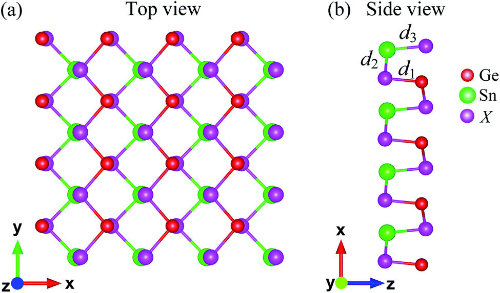
The atomic structure of Janus GeSnX2 (X = S, Se, Te) single-layers is presented in Fig. 1. The lattice constants a and b for all materials are summarized in Table 1. It is found that the lattice constants a and b (along the x and y axes, respectively) increase with an increase in the size of the X element, from S to Te. For each single-layer, the lattice a is larger than b. That is similar to the other orthorhombic structure in that the lattice parameter along the x-axis (armchair direction) is longer than that along the y-axis.42 As shown in Table 1, Janus GeSnX2 has a low directional anisotropic structure that is comparable with the group IV monochalcogenides.23,42 The anisotropy parameter a/b varies from 1.15 to 1.05. The lighter the material, the larger the anisotropy parameter a/b is. The bond lengths Gn–X and Sn–X follow a similar trend for the lattice constants that these bond lengths increase as element X changes from S to Te. Calculated the bond lengths and bond angles of GeSnX2 are also presented in Table 1.
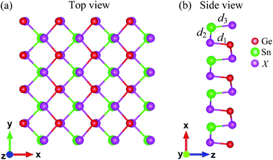 |
| | Fig. 1 Top (a) and side (b) views of atomic structure of Janus GeSnX2 (X = S, Se, Te). Ge, Sn, and X atoms are indicated by red, green, and purple balls, respectively. | |
Table 1 Lattice constants a and b, bond lengths d1,2,3, bond angle ϕ, anisotropy parameter a/b, and cohesive energy Ecoh of Janus GeSnX2 (X = S, Se, Te) single-layers
| |
a (Å) |
b (Å) |
d1 (Å) |
d2 (Å) |
d3 (Å) |
ϕ∠XSnX (deg.) |
ϕ∠GeXSn (deg.) |
a/b |
Ecoh (eV) |
| GeSnS2 |
4.42 |
3.86 |
2.41 |
2.68 |
2.60 |
90.37 |
105.09 |
1.15 |
4.42 |
| GeSnSe2 |
4.45 |
4.11 |
2.55 |
2.85 |
2.72 |
93.33 |
97.89 |
1.08 |
4.09 |
| GeSnTe2 |
4.60 |
4.38 |
2.76 |
3.05 |
2.91 |
97.20 |
91.22 |
1.05 |
3.74 |
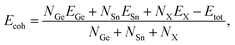
To test the strength of the covalent bond in the Janus GeSnX2 structures, we calculate their cohesive energy Ecoh as the following:
| |
 | (1) |
where
EGe,
ESn, and
EX indicate the single-atom energies of the elements Ge, Sn, and X, respectively,
Etot stands for the total energy of GeSnX
2 monolayer; and
NGe,
NSn, and
NX are the number atoms of the Ga, S, and X in the unit-cell. Our calculated results demonstrate that all three monolayers of GeSnX
2 are energetically favorable. The calculated results for the cohesive energy of GeSnX
2 monolayers are also presented in
Table 1. The
Ecoh of GeSnX
2 is form 3.74 to 4.42 eV per atom, which is comparable with that of the group IV monochalcogenides.
43,44
We next analyze the vibrational properties of the systems to evaluate their dynamical stability. The phonon dispersion bands of Janus GeSnX2 are presented in Fig. 2. The unit cell of GeSnX2 contains four atoms, including one Ge, one Sn, and two X atoms, therefore its phonon band consists of 12 vibrational modes. There are three acoustic vibrational modes in the low-frequency regime meanwhile nine optical are in higher frequency regimes. It is noted that, as shown in Fig. 2, the acoustic and optical vibrational modes coexist partially in the same frequency regime and no gap between acoustic and optical vibrational modes is observed in all three models of GeSnX2. This may lead to robust optical-acoustic scattering in these materials and as a result, they will have low thermal conductivity. Most importantly, the phonon diagrams of all three structures contain only positive frequencies. There are no soft modes in their phonon spectrum. This suggests that all considered configurations are dynamically stable and that they can be experimentally synthesized as free-standing sheets.
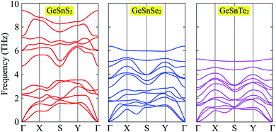 |
| | Fig. 2 Phonon spectra of Janus GeSnX2 single-layers (X = S, Se, Te). | |
3.2 Mechanical properties
In this part, we analyze the mechanical properties of Janus GeSeX2 based on the evaluations of their elastic constants Cij (using Voigt notation). The Cij constants are important parameters that can support the evaluation of elastic characteristics as well as mechanical properties of the materials. With the rectangular lattice, there are four independent constants, including C11, C12, C22, and C66. The calculated elastic constants Cij of Janus GeSnX2 single-layers are summarized in Table 2. It is found that all four Cij constants are positive, implying that the Janus GeSnX2 are mechanically stable under small in-plane deformations. Also, it can be seen that the C22 is larger than both C11 and C12, suggesting that the materials have greater rigidity in the zigzag direction (y axis). There is high anisotropy in the elastic constants of the Janus GeSnX2 single-layers. These mechanical characteristics of Janus GeSnX are similar to the group IV monochalcogenides.24
Table 2 Four independent elastic constants C11, C22, C12, and C66 of Janus GeSnX2 single-layers
| |
C11 (N m−1) |
C12 (N m−1) |
C22 (N m−1) |
C66 (N m−1) |
| GeSnS2 |
14.78 |
17.58 |
38.68 |
17.27 |
| GeSnSe2 |
19.18 |
18.92 |
40.68 |
18.52 |
| GeSnTe2 |
22.15 |
16.25 |
41.03 |
20.99 |
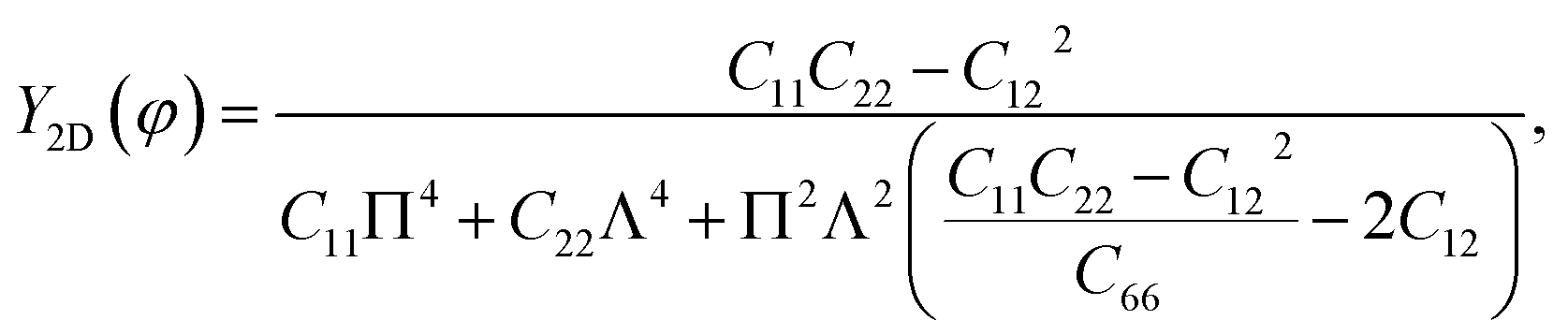
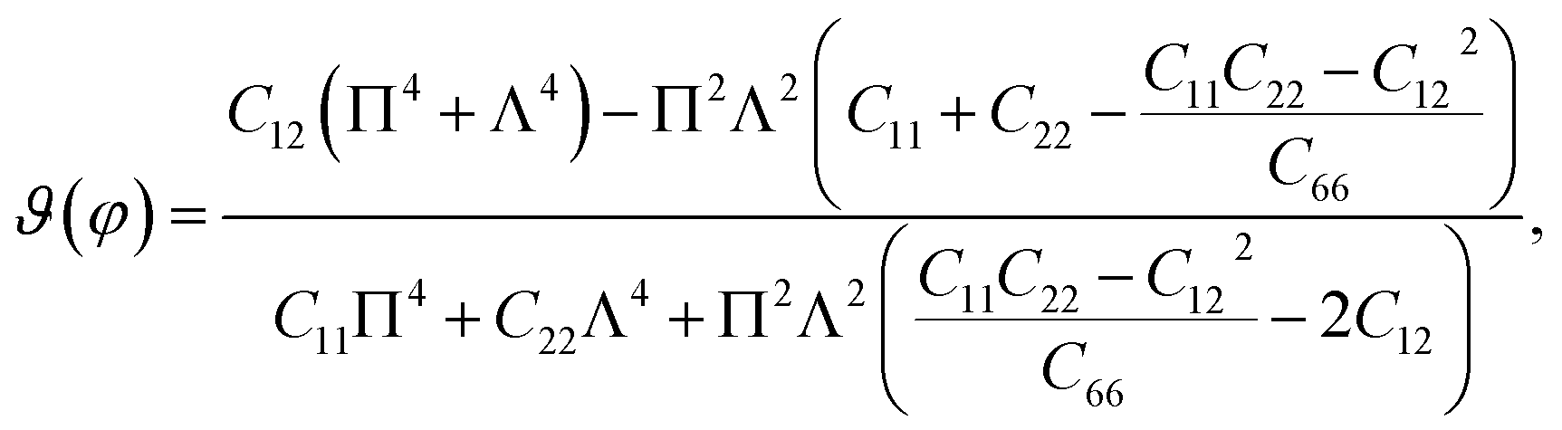
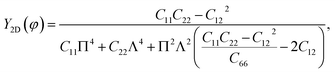
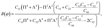
Unlike graphene or the group III monochalcogenides, the group IV monochalcogenides and also Janus group IV monochalcogenides have an anisotropic in-plane structure. Therefore, their in-plane stiffness is very sensitive to the investigated direction. The direction-dependent 2D Young's modulus Y2D(φ) and Poisson's ratio ϑ(φ) are given by34
| |
 | (2) |
| |
 | (3) |
where Π =
![[thin space (1/6-em)]](https://www.rsc.org/images/entities/char_2009.gif)
sin
φ and Λ =
cos
φ with
φ is the polar angle relative to the
x-axis (armchair direction).
From atomic structures, as shown in Fig. 1, we can qualitatively predict that the Janus GeSnX2 is the softest along the armchair direction (the x axis). This prediction is consistent with calculated results as presented in Table 2. This prediction is supported by the polar diagrams of Y2D(φ) and ϑ(φ) in Fig. 3. It is demonstrated that the mechanical characteristics of GeSnX2 are highly directional anisotropic. We can see that Y2D along the armchair direction Y2D(0°) is the smallest. It is calculated that the Y2D(0°) for GeSnS2, GeSnSe2, and GeSnTe2 single-layers is 6.63, 10.42, and 15.72 N m−1, respectively. Meanwhile, the Young's modulus along the zigzag direction Y2D(90°) is higher than Y2D(0°). From Fig. 3(a), it can be seen that the GeSnX2 is the hardest corresponding to about ±54° relative to the armchair direction. The maximum Y2D for GeSnS2, GeSnSe2, and GeSnTe2 is 40.86, 43.77, and 46.13 N m−1, respectively. GeSnX2 single-layers have a very low in-plane stiffness, which is comparable with the group IV monochalcogenide single-layers.24 Young's modulus of GeSnX2 single-layers is lower than that of similar 2D structures, such as boron–carbon–nitride (291 N m−1),45 MoS2 (130 N m−1),46 Janus group III monochalcogenides.31 This implies that GeSnX single-layers are more flexible and could be useful for applications in nanoelectromechanical devices. Similarly, Janus GeSnX2 has a high anisotropic Poisson's ratio ϑ(φ). The Poisson's ratio depends strongly on the investigated direction of the single-layers. It is found that, as presented in Fig. 3(b), the Poisson's ratio along the zigzag direction ϑ(90°) is the highest. Meanwhile, the Poisson's ratio along the ±45° relative to the armchair direction is the smallest.
 |
| | Fig. 3 Directional dependence of Young's modulus (a) and Poisson's ratio (b) of Janus GeSnX2 single-layer. | |
3.3 Electronic properties
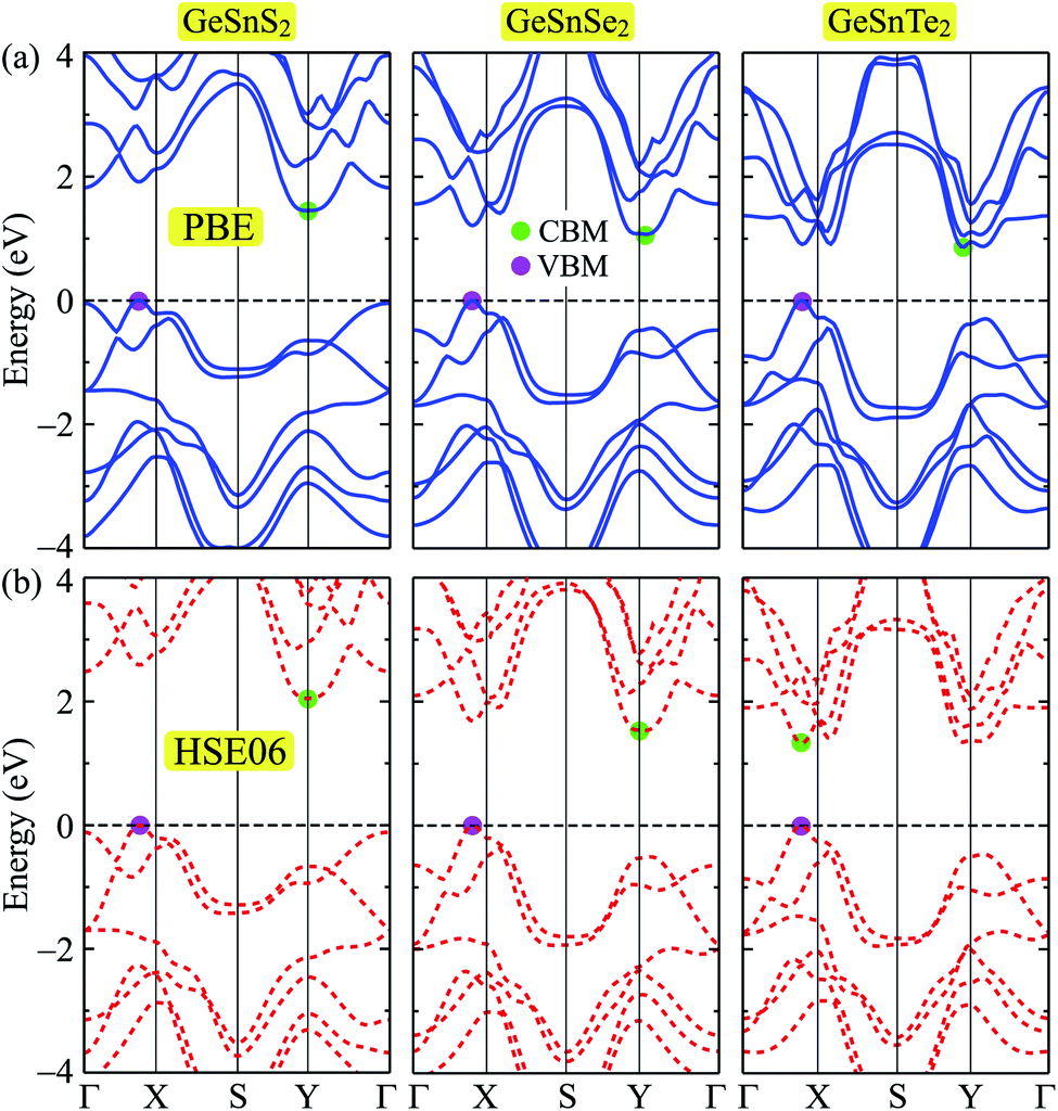
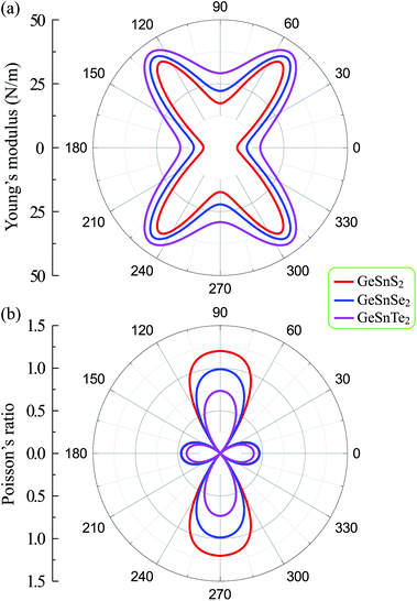
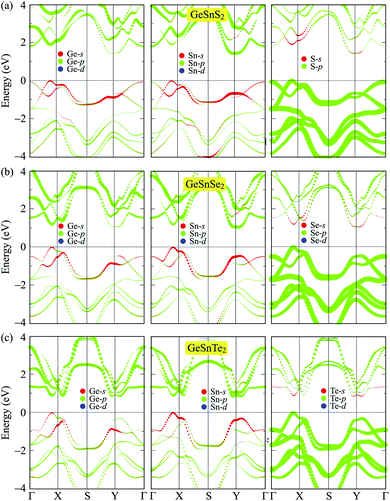
In this part, we present our calculations for the electronic properties of Janus single-layers GeSnX2 (X = S, Se, Te). It is demonstrated that all three models of GeSnX2 are semiconductors. The band structures of GeSnX2 plotted along the Γ–X–S–Y–Γ high-symmetry direction are depicted in Fig. 4. At the PBE level, all three models of GeSnX2 have an indirect bandgap with a value between 0.87 and 1.45 eV. The calculated results for the bandgap are summarized in Table 3. As shown in Fig. 4(a), the conduction band minimum (CBM) lies around the Y-point, while the valence band maximum (VBM) locates on the ΓX-path. In the case of GeSnS2, the difference in energy at the VBM and Γ-point is very small, just only 0.05 eV. Meanwhile, the difference in energy at the CBM and another lowest point on the ΓX-path of the Janus GeSnTe2 is even smaller (0.04 eV). It suggests that the electronic characteristics can be greatly modified when subjected to external influences such as mechanical strains or pressure. However, we know that the PBE method underestimates the energy gap precision. Therefore, we need to correct the electronic structure to achieve a more precise band gap value. The current popular and accurate method for energy structure correction is the HSE06 method. The band structures at the HSE06 level are presented in Fig. 4(b). It is found that the band diagrams evaluated by the PBE and HSE06 approaches are almost the same in profile. However, band structure correction with the HSE06 not only changes the bandgap of the single-layers but also changes the character of GeSnTe2, that is, GeSnTe2 has become a direct semiconductor at the HSE level despite the difference in energy between the old and new CBM positions is very small. The bandgap at the HSE06 level of GeSnS2, GeSnSe2, and GeSnTe2 is 2.05, 1.53, and 1.33 eV, respectively.
 |
| | Fig. 4 Band structures of GeSnS2, GeSnSe2, and GeSnTe2 single-layers at the PBE (a) and HSE06 (b) levels. | |
Table 3 Band gaps at the PBE and HSE06 levels, vacuum level difference ΔΦ, work functions on the XGe-side Φ1 and SnX-side Φ2 of Janus GeSnX2 single-layers. All parameters are in units of eV
| |
EPBEg |
EHSE06g |
ΔΦ |
Φ1 |
Φ2 |
| GeSnS2 |
1.45 |
2.05 |
0.46 |
4.79 |
5.25 |
| GeSnSe2 |
1.07 |
1.53 |
0.42 |
4.55 |
4.96 |
| GeSnTe2 |
0.87 |
1.33 |
0.31 |
4.46 |
4.77 |
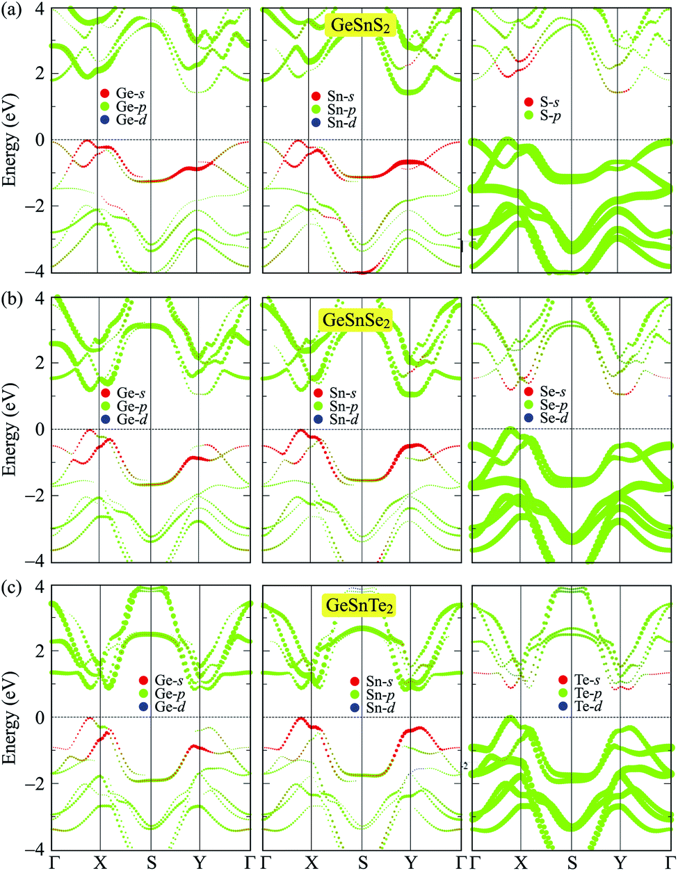
To get more insight onto the formation of electronic bands, we calculate the weighted bands of the considered systems using the PBE method. Fig. 5 presents the calculated weighted bands of GeSnX2 single-layers. In general, the projected bands of the three single-layers are quite similar. The valence band is formed by the main contribution from the p-orbitals of the X atoms, while the p-orbitals of both Ge and Sn atoms are the main contributor to the conduction band. Besides, the s-orbitals of Ge and Sn atoms contribute slightly to the valence band in the vicinity of the Fermi level. The contribution of the X-p orbitals to the conduction band is much smaller than their contribution to the valence band. It is found that VBM is contributed mainly from the p-orbitals of X atom. Ge-s and Sn-s orbitals also contribute to the formation of the VBM, however, their contribution is much smaller than that of X-s orbitals. Meanwhile, the CBM is contributed mainly from p-Ge and p-Sn orbitals and their contribution to the CBM is quite even.
 |
| | Fig. 5 Weighted bands of GeSnS2 (a), GeSnSe2 (b), and GeSnTe2 (c) at the PBE level. | |
One of the other important features of electrons that we examine in this section is the work function. The work function is a physical quantity that characterizes the ability of an electron to escape from the material surfaces. The work function Φ is calculated based on the Fermi level EF and vacuum level Evac via the relationship Φ = Evac − EF. It is noted that there exists an intrinsic built-in electric field in Janus materials due to their vertical asymmetrical structure.35 Hence, dipole correction should be included to treat the errors caused by the periodic boundary conditions.47 Planar average electrostatic potentials of GeSnX2 single-layers are shown in Fig. 6. It is found that there is a distinct vacuum level difference ΔΦ existing on the two different sides of asymmetry Janus single-layers, which does not exist in the 2D vertical symmetric materials such as monochalcogenides or dichalcogenides. This results in different work functions on the two sides of the material. The calculated results for the vacuum level difference ΔΦ and work functions on the XGe-side Φ1 and SnX-side Φ2 of Janus GeSnX2 single-layers are summarized in Table 3. We can see that the work function on the XGe-side Φ1 is slightly smaller than that on the SnX-side Φ2. It suggests that it is easier for the electron to escape from the XGe-side than from SnX-side.
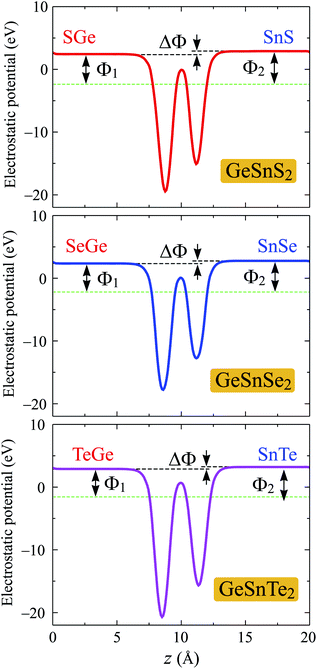 |
| | Fig. 6 Planar average electrostatic potentials of GeSnX2 single-layers. ΔΦ is the difference in vacuum level between the two sides of single-layer. | |
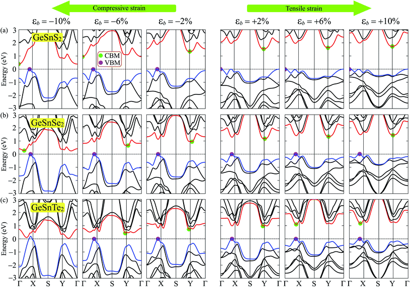
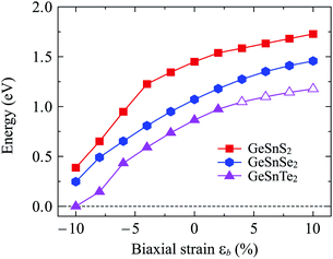
Mechanical strain is one of the simplest and most efficient ways to modify the electronic states of a material. Here, we investigate the effect of biaxial strain εb on the electronic characteristics of GeSnX2 single-layers through the PBE method. The band structures of GeSnX2 single-layers under various values of the biaxial strain εb are depicted in Fig. 7. We can see that the band structures of the considered single-layers are strongly altered when the biaxial strain was introduced. As expected, the biaxial strain significantly changes the electronic bands near the Fermi level. As a result, there is a change in the band edge positions. From Fig. 7(a and b), we see that the CBM of GeSnS2 and GeSnSe2 tends to shift from the Y-point to the Γ point in the Brillouin region when the compressive strain is applied. Meanwhile, the tensile strain caused the CBM of the GeSnTe2 to leave the Y point and come to lie on the ΓX path as shown in Fig. 7(c). Consequently, an indirect–direct bandgap transition is observed in GeSnTe2 in the presence of tensile strain. GeSnTe2 becomes direct semiconductor at εb = 4% with both CBM and VBM located on the ΓX path. The strain engineering not only changes the band edge positions but also drastically modulates their bandgap. Strain-dependent band gaps of Janus GeSnX2 single-layers are shown in Fig. 8. It is found that while the tensile strain slightly increases the bandgap of the considered single-layers, the bandgap of all three single-layers decreases rapidly when the tensile strain is applied. Interestingly, the semiconductor–metal phase transition is found in GeSnTe2 as its bandgap reduces to zero at εb = −10%. With electronic characteristics that are easily altered by strain engineering, GeSnTe2 single-layers have great prospects for applications in nanoelectromechanical devices.
 |
| | Fig. 7 Band diagrams of GeSnS2 (a), GeSnSe2 (b), and GeSnTe2 (c) under biaxial strain with various values of εb. | |
 |
| | Fig. 8 Strain-dependent band gaps of Janus GeSnX2 single-layers. Open and filled markers stand for the direct and indirect band gap, respectively. | |
4 Conclusion
In conclusion, the structural, mechanical, and electronic properties of Janus GeSnX2 single-layers have been systematically investigated by the DFT calculations. The obtained results demonstrated that all three structures of GeSnX2 are stable and they exhibits highly anisotropic mechanical characteristics due to their orthorhombic lattice. At the ground state, GeSnX2 single-layers are semiconductors with bandgap varying from 0.87 to 1.45 eV at the PBE level and from 1.33 to 2.05 eV at the HSE06 level. More interestingly, both indirect–direct bandgap and semiconductor–metal phase transition are observed in GeSnX2 when the biaxial strain is applied. With its mechanical flexibility and electronic properties easily controlled by strain engineering, GeSnX2 single-layers are predicted to be materials with many promising applications in nanoelectromechanical devices.
Conflicts of interest
There are no conflicts to declare.
References
- K. Khan, A. K. Tareen, M. Aslam, R. Wang, Y. Zhang, A. Mahmood, Z. Ouyang, H. Zhang and Z. Guo, J. Mater. Chem. C, 2020, 8, 387–440 RSC
 .
. - N. A. Poklonski, S. A. Vyrko, A. I. Siahlo, O. N. Poklonskaya, S. V. Ratkevich, N. N. Hieu and A. A. Kocherzhenko, Mater. Res. Express, 2019, 6, 042002 CrossRef .
- L. Seixas, J. Appl. Phys., 2020, 128, 045115 CrossRef CAS .
- S. Barraza-Lopez, B. M. Fregoso, J. W. Villanova, S. S. Parkin and K. Chang, Rev. Mod. Phys., 2021, 93, 011001 CrossRef CAS .
- K. S. Novoselov, A. K. Geim, S. V. Morozov, D. Jiang, Y. Zhang, S. V. Dubonos, I. V. Grigorieva and A. A. Firsov, Science, 2004, 306, 666 CrossRef CAS PubMed .
- B. Lalmi, H. Oughaddou, H. Enriquez, A. Kara, S. Vizzini, B. Ealet and B. Aufray, Appl. Phys. Lett., 2010, 97, 223109 CrossRef .
- A. Acun, L. Zhang, P. Bampoulis, M. Farmanbar, A. van Houselt, A. N. Rudenko, M. Lingenfelder, G. Brocks, B. Poelsema, M. I. Katsnelson and H. J. W. Zandvliet, J. Phys.: Condens. Matter, 2015, 27, 443002 CrossRef CAS PubMed .
- F. Feng Zhu, W. Jiong Chen, Y. Xu, C. Lei Gao, D. Dan Guan, C. Hua Liu, D. Qian, S.-C. Zhang and J. Feng Jia, Nat. Mater., 2015, 14, 1020–1025 CrossRef PubMed .
- D. Kong, H. Wang, J. J. Cha, M. Pasta, K. J. Koski, J. Yao and Y. Cui, Nano Lett., 2013, 13, 1341–1347 CrossRef CAS PubMed .
- S. M. Yoon, H. J. Song and H. C. Choi, Adv. Mater., 2010, 22, 2164–2167 CrossRef CAS PubMed .
- C. Li, L. Huang, G. P. Snigdha, Y. Yu and L. Cao, ACS Nano, 2012, 6, 8868–8877 CrossRef CAS PubMed .
- L. A. Burton, D. Colombara, R. D. Abellon, F. C. Grozema, L. M. Peter, T. J. Savenije, G. Dennler and A. Walsh, Chem. Mater., 2013, 25, 4908–4916 CrossRef CAS .
- T. N. Bich, S. S. Kubakaddi, L. Dinh, N. N. Hieu and H. V. Phuc, Phys. Rev. B, 2021, 103, 235417 CrossRef CAS .
- K. D. Pham, N. N. Hieu, H. V. Phuc, I. A. Fedorov, C. A. Duque, B. Amin and C. V. Nguyen, Appl. Phys. Lett., 2018, 113, 171605 CrossRef .
- H. T. T. Nguyen, M. M. Obeid, A. Bafekry, M. Idrees, T. V. Vu, H. V. Phuc, N. N. Hieu, L. T. Hoa, B. Amin and C. V. Nguyen, Phys. Rev. B, 2020, 102, 075414 CrossRef CAS .
- P. T. Huong, D. Muoi, H. V. Phuc, C. V. Nguyen, L. T. Hoa, B. D. Hoi and N. N. Hieu, J. Mater. Sci., 2020, 55, 14848–14857 CrossRef CAS .
- C. V. Nguyen, N. N. Hieu, N. A. Poklonski, V. V. Ilyasov, L. Dinh, T. C. Phong, L. V. Tung and H. V. Phuc, Phys. Rev. B, 2017, 96, 125411 CrossRef .
- T. V. Vu, H. V. Phuc, S. Ahmad, V. Q. Nha, C. V. Lanh, D. P. Rai, A. I. Kartamyshev, K. D. Pham, L. C. Nhan and N. N. Hieu, RSC Adv., 2021, 11, 23280–23287 RSC .
- T. V. Vu, H. V. Phuc, C. V. Nguyen, A. I. Kartamyshev and N. N. Hieu, J. Phys. D: Appl. Phys., 2021, 54, 475306 CrossRef CAS .
- Z. Hu, Y. Ding, X. Hu, W. Zhou, X. Yu and S. Zhang, Nanotechnology, 2019, 30, 252001 CrossRef CAS PubMed .
- L. Makinistian and E. A. Albanesi, Phys. Rev. B: Condens. Matter Mater. Phys., 2006, 74, 045206 CrossRef .
- L. Makinistian and E. A. Albanesi, J. Phys.: Condens. Matter, 2007, 19, 186211 CrossRef CAS PubMed .
- C. Chowdhury, S. Karmakar and A. Datta, J. Phys. Chem. C, 2017, 121, 7615–7624 CrossRef .
- R. Fei, W. Li, J. Li and L. Yang, Appl. Phys. Lett., 2015, 107, 173104 CrossRef .
- A.-Y. Lu, H. Zhu, J. Xiao, C.-P. Chuu, Y. Han, M.-H. Chiu, C.-C. Cheng, C.-W. Yang, K.-H. Wei, Y. Yang, Y. Wang, D. Sokaras, D. Nordlund, P. Yang, D. A. Muller, M.-Y. Chou, X. Zhang and L.-J. Li, Nat. Nanotechnol., 2017, 12, 744 CrossRef CAS PubMed .
- J. Zhang, S. Jia, I. Kholmanov, L. Dong, D. Er, W. Chen, H. Guo, Z. Jin, V. B. Shenoy, L. Shi and J. Lou, ACS Nano, 2017, 11, 8192–8198 CrossRef CAS PubMed .
- M. J. Varjovi, M. Yagmurcukardes, F. M. Peeters and E. Durgun, Phys. Rev. B, 2021, 103, 195438 CrossRef CAS .
- R. Peng, Y. Ma, S. Zhang, B. Huang and Y. Dai, J. Phys. Chem. Lett., 2018, 9, 3612 CrossRef CAS PubMed .
- T. V. Vu, C. V. Nguyen, H. V. Phuc, A. A. Lavrentyev, O. Y. Khyzhun, N. V. Hieu, M. M. Obeid, D. P. Rai, H. D. Tong and N. N. Hieu, Phys. Rev. B, 2021, 103, 085422 CrossRef CAS .
- M. Demirtas, B. Ozdemir, Y. Mogulkoc and E. Durgun, Phys. Rev. B, 2020, 101, 075423 CrossRef CAS .
- T. V. Vu, V. T. T. Vi, H. V. Phuc, A. I. Kartamyshev and N. N. Hieu, Phys. Rev. B, 2021, 104, 115410 CrossRef CAS .
- T. V. Vu, V. T. T. Vi, H. V. Phuc, C. V. Nguyen, N. A. Poklonski, C. A. Duque, D. P. Rai, B. D. Hoi and N. N. Hieu, J. Phys.: Condens. Matter, 2021, 33, 225503 CrossRef CAS PubMed .
- J. Qiu, F. Zhang, H. Li, X. Chen, B. Zhu, H. Guo, Z. Ding, J. Bao and J. Yu, IEEE Electron Device Lett., 2021, 42, 561–564 CAS .
- P. Nandi, A. Rawat, R. Ahammed, N. Jena and A. De Sarkar, Nanoscale, 2021, 13, 5460 RSC .
- C.-F. Fu, J. Sun, Q. Luo, X. Li, W. Hu and J. Yang, Nano Lett., 2018, 18, 6312–6317 CrossRef CAS PubMed .
- P. Giannozzi, S. Baroni, N. Bonini, M. Calandra, R. Car, C. Cavazzoni, D. Ceresoli, G. L. Chiarotti, M. Cococcioni, I. Dabo, A. Dal Corso, S. de Gironcoli, S. Fabris, G. Fratesi, R. Gebauer, U. Gerstmann, C. Gougoussis, A. Kokalj, M. Lazzeri, L. Martin-Samos, N. Marzari, F. Mauri, R. Mazzarello, S. Paolini, A. Pasquarello, L. Paulatto, C. Sbraccia, S. Scandolo, G. Sclauzero, A. P. Seitsonen, A. Smogunov, P. Umari and R. M. Wentzcovitch, J. Phys.: Condens. Matter, 2009, 21, 395502 CrossRef PubMed .
- G. Kresse and D. Joubert, Phys. Rev. B: Condens. Matter Mater. Phys., 1999, 59, 1758 CrossRef CAS .
- J. Heyd, G. E. Scuseria and M. Ernzerhof, J. Chem. Phys., 2003, 118, 8207 CrossRef CAS .
- S. Grimme, J. Comput. Chem., 2006, 27, 1787 CrossRef CAS PubMed .
- H. J. Monkhorst and J. D. Pack, Phys. Rev. B: Solid State, 1976, 13, 5188 CrossRef .
- T. Sohier, M. Calandra and F. Mauri, Phys. Rev. B, 2017, 96, 075448 CrossRef .
- Y. Guo, S. Zhou, Y. Bai and J. Zhao, ACS Appl. Mater. Interfaces, 2017, 9, 12013–12020 CrossRef CAS PubMed .
- Y. Xu, H. Zhang, H. Shao, G. Ni, J. Li, H. Lu, R. Zhang, B. Peng, Y. Zhu, H. Zhu and C. M. Soukoulis, Phys. Rev. B, 2017, 96, 245421 CrossRef .
- A. K. Deb and V. Kumar, Phys. Status Solidi B, 2016, 254, 1600379 CrossRef .
- S. Thomas and M. A. Zaeem, Phys. Chem. Chem. Phys., 2020, 22, 22066–22077 RSC .
- R. C. Cooper, C. Lee, C. A. Marianetti, X. Wei, J. Hone and J. W. Kysar, Phys. Rev. B: Condens. Matter Mater. Phys., 2013, 87, 035423 CrossRef .
- L. Bengtsson, Phys. Rev. B: Condens. Matter Mater. Phys., 1999, 59, 12301–12304 CrossRef CAS .
|
| This journal is © The Royal Society of Chemistry 2021 |
Click here to see how this site uses Cookies. View our privacy policy here. 
 Open Access Article
 This Open Access Article is licensed under a Creative Commons Attribution-Non Commercial 3.0 Unported Licence
 *
*