
 Open Access Article
 This Open Access Article is licensed under a Creative Commons Attribution-Non Commercial 3.0 Unported Licence
The synthesis of CdZnTe semiconductor thin films for tandem solar cells
Nazar Abbas Shah *a,
Waqar Mahmoodb,
Murrawat Abbasc,
Nadeem Nazard,
Ashfaq H. Khosaa,
Aurang Zebd and
Abdul Malike
*a,
Waqar Mahmoodb,
Murrawat Abbasc,
Nadeem Nazard,
Ashfaq H. Khosaa,
Aurang Zebd and
Abdul Malike
aDepartment of Physics, COMSATS University, Park Road, Islamabad, 44000, Pakistan. E-mail: ashfaq_khosa@comsats.edu.pk; nazar_abbas@comsats.edu.pk; Tel: +92-0321-5105363
bMaterial Synthesis & Characterizations Laboratory, Department of Physics, Fatima Jinnah Women University, The Mall, Rawalpindi, 46000, Pakistan. E-mail: waqarmahmood@fjwu.edu.pk
cDepartment of Physics, Islamic International University, Islamabad, Pakistan. E-mail: murrawatshah01@gmail.com
dFederal Urdu University of Arts Science and Technology, Islamabad, 44000, Pakistan. E-mail: nnsi192@yahoo.com; aurangzebbabar@yahoo.com
eNational Institute of Lasers and Optics, Islamabad, Pakistan. E-mail: abdulmalik461@gmail.com
First published on 15th December 2021
Abstract
A new approach is adopted to grow cadmium zinc telluride (CdZnTe) thin films using the close spaced sublimation (CSS) technique. The deposition parameters for the growth of cadmium telluride (CdTe) thin films onto the glass substrate were optimized. A zinc telluride (ZnTe) thin film layer was deposited onto already-deposited CdTe thin film to fabricate the CdZnTe (CZT) thin film sample as a ternary compound. Annealing was done after the successful deposition of CZT thin films before further characterization of the CZT thin film samples. The structures of the CZT thin film samples were studied using X-ray diffraction (XRD) and cubic phases were found. A spectrophotometer was used to study the optical parameters, and the energy band gap was found to be in the range of 1.45 eV to 1.75 eV after annealing. The nature of the direct band gap predicts that it might be an ideal component in second-generation solar cells. A Hall measurement system was used to find that the electrical conductivity was in the range of 4.6 × 10⁻⁶ to 8.2 × 10⁻¹¹ (ohm cm)−1. XPS analysis confirmed the presence of Zn in the CdTe thin films. A significant change in electronic properties was observed. These results show that these CZT thin film samples can not only play a key role in the tandem structures of high-efficiency solar cells but they could also be used in the detection of X-rays and gamma rays.
Introduction
Thin films play a significant role in science and are important due to high-tech electronics, computers and photovoltaic industries. The technology developed for thin films was used for the primary need for integrated circuit (IC) industries. Furthermore, high-speed devices with a smaller size of ICs require materials with the latest synthesis techniques for gig integration scale (GIS) in future. The above-mentioned goal can be achieved using the physics of thin film technology.1–3In the last few decades, the structural, electrical and optical parameters of CdTe, its alloys and compounds, have been studied extensively because of the large number of applications in opto-electronics. Different metals are used as dopants in CdTe thin films and produce remarkable changes in physical properties that actually make it suitable for thin film technology and devices.2 Among such dopants in CdTe thin films, ternary alloy IIB–VIA semiconductor compound CdZnTe (CZT) thin films are selected and analyzed to study different applications in the thin film technology of X-ray and γ-ray detectors and also in tandem soler cell technology.4–7
CZT ternary compounds have a direct energy band gap which varies from the 1.45 eV of CdTe to the 2.24 eV of ZnTe with an increase in Zn-concentration.8 The attention paid to CZT thin films is due to their band gap energy from 1.45 eV to 1.76 eV, which is suitable for a variety of applications in optoelectronics and in tandem solar cells.9
A variety of techniques have been adopted to grow II–VI compound semiconductor thin films, like e-beam evaporation,1 high vacuum thermal evaporation,2,3 molecular beam epitaxy, MBE,4 electro-deposition,5 spray pyrolysis and solution growth,6,7 chemical vapor deposition8 and close spaced sublimation.10–16
In the current work, CZTs are synthesized by the close spaced sublimation (CSS) technique by using a multilayer method. A tunable energy band gap of CZT, depending upon Zn contents, is observed ranging from 1.45 to 2.24 eV. This is a favorite photovoltaic part in a tandem solar cell due to its engineered energy band gap from the visible (VIS) to the infrared (IR) region of light.17–19 In epitaxial growth, CZT was used as a substrate for mercury cadmium telluride (HgCdTe) and Cd0.96Zn0.04Te. It exactly matched the lattice parameters to long wavelength for infrared HgCdTe (80% Hg, 20% Cd). One of the issues was its large crystal growth with set compositions. CdTe and ZnTe have lattice constants in the (111) direction of 6.481 and 6.104 nm, respectively.20
The lattice constant of CZT and energy band gap can be engineered by adding a nominal amount of ZnTe to CdTe thin films. CZT thin films can be grown using the closed space sublimation technique, rf-sputtering,21 molecular beam epitaxy22 etc. for use in solar cell applications.23,24 The energy gap of this ternary compound is tunable for solar cell applications. A new approach was adopted to grow cadmium zinc telluride (CdZnTe) thin films using the close spaced sublimation technique for the first time in our research lab.
Research methodology
In the closed space sublimation (CSS) technique for deposition, the growth of a CdTe thin film can be understood with the reaction at high temperature,| 2CdTe(s) ⇔ 2Cd(g) + Te2(g) |
The optimized distance between the CdTe source and a substrate was kept at 5 mm. CdTe dissociates into Cd and Te contents at high temperature which recombine on a low-temperature substrate surface.
Cadmium telluride (CdTe) 99.99% was used in a graphite boat as a source material. A glass slide was used as a substrate material after cleaning in an ultrasonic bath at a temperature of 60 °C with IPA for 20 min. The source material and cleaned substrate were placed in a vacuum evaporation chamber with a mica sheet used as a separator between source and substrate. A slab of graphite was put onto the substrate surface for uniform heating. Two K-type thermocouples were introduced and attached to source and substrate temperature controllers during the evaporation process to monitor the temperatures. Halogen lamps of 1000 W and 500 W were attached for source and substrate heating. The whole setup was covered with a bell jar before creating the vacuum. A rotary pump and an oil diffusion pump with gauges were introduced for a rough vacuum and a high vacuum down to 10−5 mbar. Once the required level of vacuum was achieved, the source and substrate lamps were switched on and the temperatures gradually increased and were controlled using temperature controllers. The source temperature was maintained at 550 °C and the substrate at 350 °C and the growth times for CdTe thin films were kept at 2, 3 and 5 minutes. After the successful growth of CdTe thin films for a specific deposition time, the source lamp was switched off and the substrate lamp was kept on until the source temperature had come down to that of the substrate for uniform heating. The vacuum was broken and the chamber was opened when the source and substrate temperature reached below 40 °C after disconnecting all the electrical connections.
In the next step, ZnTe was used as a source material and the substrates of CdTe thin film were used as a substrate. The source and substrate temperatures were kept at 480 °C and 300 °C under a high vacuum of 10−4 mbar. The annealing process was carried out under 10−2 mbar for different temperatures and times to optimize the best temperature and time for the improved crystallinity of CdZnTe (CZT) thin film samples. It was observed that the CZT thin films showed uniformity and good adhesion after performing a tape test on these films. Another observation was that due to Cd and Zn atoms diffusing into CdTe thin film samples, there was a color change from gray to blackish gray in the CZT thin film samples.
These CZT thin film samples were cut with a diamond cutter into small pieces for further characterization. The structural study was carried out using X-ray diffraction (XRD) and the thickness with composition was checked using Rutherford backscattering (RBS). Scanning electron microscopy (SEM) and energy dispersive X-rays (EDX) were implemented for a surface morphological study. A spectrophotometer was used to measure the optical parameters. A Hall measurements system was further used to check the electrical parameters. Similarly, atomic force microscopy (AFM) and X-ray photoelectron spectroscopy (XPS) were used to study the surface roughness and electronics configurations, respectively.
Results and discussion
X-ray diffraction study
Studies of the structural parameters of the ZnTe, CdTe and CZT thin film samples were carried out using X-ray diffraction (XRD). Cu-Kα radiation with a wavelength of 1.5418 Å was used to create the diffraction patterns, as shown in Fig. 1 and 2. | ||
| Fig. 1 (a) The XRD pattern of CdTe thin film and the (b) XRD spectrum of ZT-1 thin film. | ||
 | ||
| Fig. 2 XRD patterns of CZT samples (a–d) annealed at 100 °C. | ||
The XRD pattern for CdTe thin films shown in Fig. 1(a) has main peaks and indexed Bragg's angles at 23.8065°, 23.7750°, 23.7117°, 23.8924° and 23.7307°, respectively, for five selected samples with optimized growth parameters. The peaks were confirmed from the ASTM data sheet. The preferred orientation for all the CdTe thin films was the [111] direction in the cubic phase. The other two peaks [220] and [331] also belonged to the cubic phase but they have very low intensity compared to the preferred orientation. This confirmed that the CdTe thin films were polycrystalline in nature and this is also well documented in the literature.1 That the values of the full width at half maxima (FWHM) are broadened for these CdTe thin films reflects the fine crystallinity deposited by the CSS technique. The other structural parameters for the preferred orientations for the CdTe thin films were calculated and it was found that the lattice parameter for [111] ranges from 6.4509 to 6.4993 nm and the grain sizes, dislocation density and micro-strain are the same for these selected CdTe thin films.
It was observed that the CZT thin film samples were amorphous due to the irregular arrangement of Cd and Zn atoms on the lattice sites. It might be possible that Zn atoms impart all their energies during deposition on CdTe thin film samples for adhesion and are unable to arrange themselves on the sites of the lattice. CZT thin film samples were cut into 2 cm × 2 cm size pieces and annealed under optimized 10−4 mbar vacuum with temperatures of 100 °C, 200 °C, 300 °C and 400 °C for 20 minutes. Annealing helped the Cd and Zn atoms to reach the proper place on the lattice site to make a stable and regular arrangement for the crystal structure.
With 100 °C annealing, the CZT thin film samples showed a good crystal structure compared to 200 °C. The crystal structure became amorphous at 300 °C due to excess thermal energy for Cd and Zn atoms on the lattice sites. The Cd and Zn atoms may become free with a thermal energy of 300 °C and leave the lattice site. It is also possible that some other complex structures were formed.
Fig. 2 shows the XRD spectra of CZT thin film samples annealed at 100 °C with diffraction peaks at 2θ = 25.0216°, 41.5503°, 49.0676°, 60.1934° and 66.0859°. It is important to mention that all the peaks are indexed in the cubic structure, as confirmed from Vegard's law and the ASTM data sheet.2 The growth of the CZT thin film samples was confirmed with Vegard's law.
The cubic structure could be confirmed from the peaks for (111), (220), (311), (400) and (331). It is also evident that the CZT thin film samples were polycrystalline in nature with the (111) direction as a preferred orientation. The composition ‘x’ of Cd1−xZnxTe was found with the help of Vegard's law, and the lattice constant for CZT thin film samples, particularly for cubic peaks, changes linearly from CdTe to ZnTe with ‘x’ composition.3

The lattice constant for CdTe is 6.4823 nm, whereas the lattice constant for ZnTe is 6.0500 nm. Vegard's law helped us to calculate the value of ‘x’ and we found it to be 0.85 for our experimental value. This value depicts a cubic structure for enriched CZT thin film samples. The peaks are slightly shifted towards the lower Bragg's angle for the CZT thin film samples, as shown Fig. 2. The substitution of a Cd atom for a Zn atom might be the reason for this shift on the surface before annealing. The deposition process involving the substitution of a Cd atom and annealing is mainly responsible for the growth of the CZT structure. Small peaks can be seen at 23.9004°, 23.9127°, 23.7660° and 23.7841°, respectively, in the XRD spectra of Fig. 2. These peaks were the minor phases of the CZT thin film samples. A low concentration of Zn was also found in these samples and they are further analyzed using Rutherford backscattering (RBS) in the coming section. The low concentration of Zn showed the reactive diffusion of CdTe, which resulted in the minor phases in the CZT thin film samples. Table 1 introduces the grain sizes, dislocation density, micro-strain and the lattice constant calculations of these CZT thin film samples.
| Sample ID | Lattice constant (Å) | Grain size (Å) | Strain (1 × 10⁻⁴ ) | Dislocation density (1 × 10⁻⁵) | Structural composition “x” |
|---|---|---|---|---|---|
| CZT-1 | 6.1060 | 207.11 | 16.75 | 1.99 | 0.87 |
| CZT-2 | 6.1166 | 295.77 | 11.73 | 0.97 | 0.85 |
| CZT-2 (200 °C) | 6.1391 | 172.68 | 20.09 | 2.84 | — |
| CZT-3 | 6.1473 | 517.84 | 6.70 | 0.316 | 0.77 |
| CZT-4 | 6.1181 | 207.10 | 16.75 | 1.98 | 0.84 |
| CZT-5 | 6.1047 | 207.10 | 16.75 | 1.99 | 0.86 |
SEM study
Scanning electron microscopy (SEM) was used to study the surface morphology of the CZT thin film samples, as shown in Fig. 3(a–d). These high-resolution micrographs showed the grain orientation, smoothness and uniformity on the surface. The grain boundaries are also very clear for the CZT thin film samples. The average grain sizes vary from 200 nm to 400 nm, estimated from the scaling available in the software of the SEM machine. These grain sizes show good agreement with the calculation of particle size in the XRD study. It is also evident that the merger of small grains to form a larger grain is due to the coalescence phenomena in semiconductors.4 The larger grains of the CZT thin film samples using the CSS technique compared to other elemental methods makes the CSS technique a well-known technique for forming larger grains of semiconductor thin films with good quality. The larger grains of as-deposited and annealed CZT thin film samples strongly affect the electrical properties as well as their atomic force microscopy study. In Fig. 3(a–d), a long-shaped grain is due to the presence of Zn element on the surface, which is undiffused after annealing. | ||
| Fig. 3 SEM images of CZT samples (a–d). | ||
EDX study
The elemental composition was studied using energy dispersive X-rays (EDX) integrated with the SEM machine. The elements Zn, Te and Cd with their compositions are shown in Table 2. It is clear from Table 2 that after annealing Zn and Cd diffuse with Te to make CZT thin film samples. It is also evident from SEM that after annealing the Cd atoms move toward the upper surface of the films.| Sample ID | At% | Composition
|
||
|---|---|---|---|---|
| Zn | Cd | Te | ||
| CZT-1 | 27.66 | 25.97 | 46.55 | 0.52 |
| CZT-2 | 21.56 | 27.98 | 50.47 | 0.44 |
| CZT-3 | 29.23 | 21.55 | 49.22 | 0.58 |
| CZT-5 | 21.48 | 28.65 | 49.87 | 0.43 |
RBS study
The Rutherford backscattering (RBS) spectra of the CZT thin film samples were studied using 5 MV Pelletron tandem accelerators 5 UDH-2 with a beam energy of helium ions of 2 to 2.08 MeV. Fig. 4(a) shows the RBS spectra of the CZT thin film samples using RUMP software. The experimental data for the CdTe thin films is shown by the black line and the red line indicates the simulated data using the RUMP software of RBS. | ||
| Fig. 4 RBS spectra of (a) CdTe thin film and (b) CdZnTe thin film samples. | ||
The composition, thickness and other accelerators are the standard parameters used in the RUMP software to simulate the experimental data. The peak broadening from 1400 to 1600 shows the thickness simulation of the CdTe thin film, whereas the normalized yield simulates the composition of these thin films, as shown in Table 3. The composition of the glass substrate is also indicated by the composition of O and Si. A slightly higher concentration of Cd in thicker films was observed in CdTe thin films using the RBS study.
| Sample ID | Thickness (nm) | Composition | |
|---|---|---|---|
| Cd | Te | ||
| CT-1 | 170 | 0.50 | 0.50 |
| CT-2 | 290 | 0.49 | 0.51 |
| CT-3 | 350 | 0.50 | 0.50 |
| CT-4 | 620 | 0.52 | 0.48 |
| CT-5 | 620 | 0.52 | 0.48 |
The CZT thin film sample annealed at 100 °C is shown in Fig. 4(b), which was studied using RBS spectra. The variation in Te, Zn and Cd concentration along with the thickness of the thin films can be seen in the RBS spectra. It is observed that on the bottom layer and half the top layer, the Zn concentration is high. This is due to the deposition of CdTe onto ZnTe thin films. The concentration of Cd is high at the bottom in a similar way. The difference in concentration of Cd between the two layers with a value of 0.10 is very small compared to the concentration of Zn, i.e. 0.35. The high concentration of Zn element compared to the elements of Cd on the upper half is due to the CZT thin film samples having enriched Zn content. The low concentration of Zn content in the lower half interacts with CdTe and shows the formation of some minor phases of CZT thin film samples with maximum Cd content. These peaks of the minor phases are also discussed in the XRD study from CZT thin film samples. Table 4 shows the variation in Cd and Zn thickness and concentration in all CZT thin film samples.
| Sample ID | Total thickness (nm) | Layer 1 (top layer) | Layer 2 (bottom layer) | ||||||
|---|---|---|---|---|---|---|---|---|---|
| Thickness (nm) | Composition | Thickness (nm) | Composition | ||||||
| Cd | Zn | Te | Cd | Zn | Te | ||||
| CZT-1 | 300 | 140 | 0.30 | 0.45 | 0.25 | 160 | 0.40 | 0.10 | 0.50 |
| CZT-2 | 380 | 200 | 0.30 | 0.40 | 0.30 | 180 | 0.45 | 0.05 | 0.50 |
| CZT-3 | 440 | 200 | 0.27 | 0.43 | 0.30 | 240 | 0.48 | 0.02 | 0.50 |
| CZT-4 | 990 | 230 | 0.25 | 0.45 | 0.30 | 660 | 0.58 | 0.02 | 0.40 |
| CZT-5 | 690 | 220 | 0.22 | 0.48 | 0.30 | 470 | 0.45 | 0.05 | 0.50 |
AFM study
Atomic force microscopy (AFM) was used to study the surface quality of the CZT thin film samples. 2-D and 3-D AFM images were obtained using the tapping mode with one Newton repulsion force between the surface of the sample and the tip. In Fig. 5, a large-scale 10 × 10 micron image was obtained and its root mean square (RMS) and average roughness were calculated. The RMS value of the CZT thin film sample was 10.5 nm and the average value was 8.28 nm. Roughness values calculated through RMS values for the other samples were 24.5 nm, 24.7 nm, 23.6 nm and 15.1 nm (not shown in Fig. 5). These roughness values confirmed that the surface of the film was uniform and smooth. The increase in the thickness of the thin films would be the main cause of RMS roughness on the surface of the CZT thin film samples. It is also evident that deposition of ZnTe thin films onto the thicker CdTe thin films to make CZT thin film samples might create some defects on the surface of the thin films.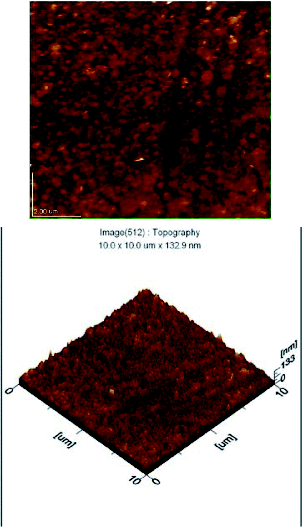 | ||
| Fig. 5 2-D (top) and 3-D (bottom) AFM images of a CZT thin film sample. | ||
Optical study
A UV-vis-NIR spectrophotometer (PerkinElmer Lamda 950) with UV WinLab software was used to obtain the transmittance data for CdTe, ZnTe and CZT thin film samples in the range of 250 nm to 2200 nm. The optical parameters like absorption coefficient, thickness, and refractive index were calculated using the Swanepoel method.4–6 The energy band gap was further calculated using the absorption coefficient in the Tauc relation.7–9Fig. 6 shows the transmittance vs. wavelength graph for CdTe thin films. It is observed that with an increase in thickness, the transmittance decreased. It is also evident that using the Swanepoel formulae for the absorption coefficient and a plot of (αhν)2 vs. the energy (hν) for the direct band gap energy using the relation αhν = (hν − Eg)m, it is found that m = ½, which is true for a direct band gap energy in semiconductors. Furthermore, extrapolating the linear portion of (αhν)2 against the energy (hν) of an incident photon at zero absorption gave the band gap energy of CdTw thin film, as shown in Fig. 6(b). The band gap energy of CdTe thin film was 1.49 eV, which is very close to the theoretical value for CdTe.
 | ||
| Fig. 6 (a) Transmission patterns of CdTe thin films. (b) The band gap energy of a CdTe thin film sample. | ||
Fig. 7(a) shows the transmittance plot of the CZT thin film sample. It is clear from Fig. 7(a) that a thinner sample of CZT has a larger value of transmission. The band gap energy of the CZT thin film samples after annealing calculated using the Swanepoel method are shown in Fig. 7(b). The refractive index and band gap energy of the CZT thin film samples are shown in Table 5. This variation might be due to the changed composition of Zn in the CZT thin film samples. These ranges of band gap energies for CZT thin film samples are suitable for the top layer of a tandem solar cell.6
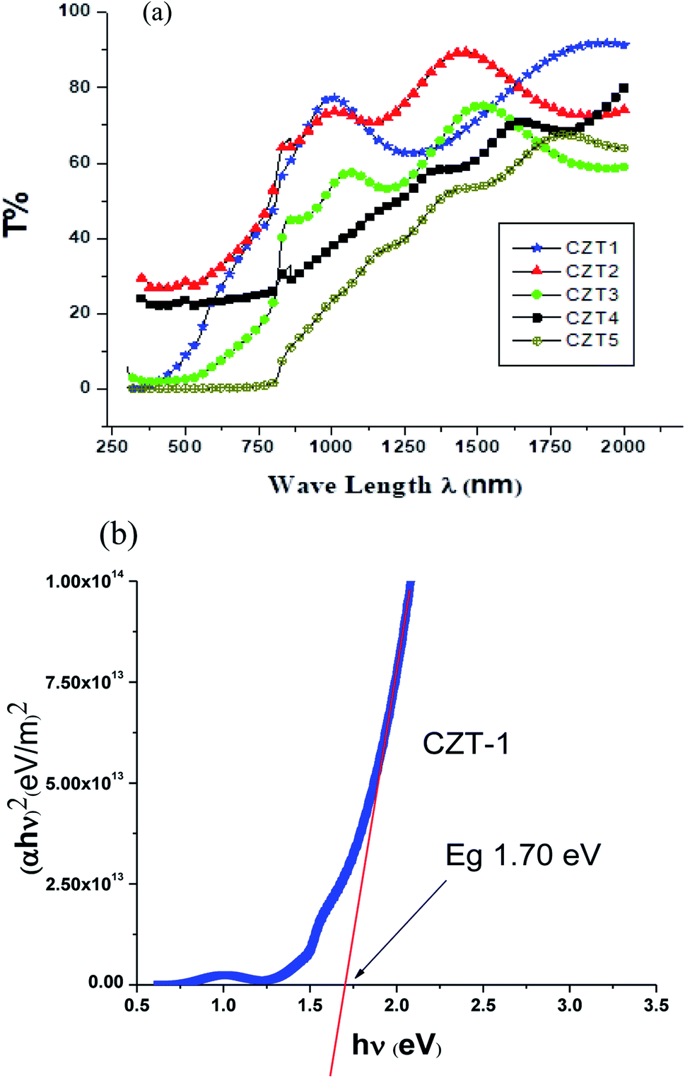 | ||
| Fig. 7 (a) Transmission patterns of CdZnTe thin film samples. (b) The band gap energy of a CdZnTe thin film sample. | ||
| Sample ID | Energy gap (eV) | Refractive index | Composition “x” |
|---|---|---|---|
| CZT-1 | 1.70 | 2.44 | 0.52 |
| CZT-2 | 1.63 | 2.05 | 0.44 |
| CZT-3 | 1.77 | 2.45 | 0.88 |
| CZT-4 | 1.60 | 2.14 | — |
| CZT-5 | 1.59 | 2.50 | 0.43 |
Electrical study
The carrier concentration, Hall coefficient, mobility, conductivity, and resistivity were calculated using a Hall measurement system (Ecopia HMS 5000). The van der Pauw method was adopted to obtain the resistivity. All measurements were carried out at room temperature. The electrical properties at room temperature are given in Table 6. The values of conductivity vary from 4.66 × 10⁻⁶ to 8.20 × 10⁻¹¹ (Ω cm)−1 which is in good agreement with the already reported data for some other techniques of deposition for CZT thin films.4–6 The higher value of resistivity confirmed that the metallic atoms (Zn & Cd) are free and are almost negligible for the formation of the CZT thin film after diffusion.7| Sample ID | Conductivity (Ω cm)−1 | Resistivity (Ω cm) | Mobility (cm2 N s) | Sheet concentration |
|---|---|---|---|---|
| CZT-1 | 2.08 × 10⁻¹⁰ | 4.80 × 10+09 | 5.29 | −7.37 × 10+03 |
| CZT-2 | 8.20 × 10⁻¹¹ | 1.22 × 10+10 | 5.23 × 10−01 | −3.72 × 10+04 |
| CZT-3 | 5.76 × 10⁻¹¹ | 1.74 × 10+10 | 4.37 × 10−01 | −3.62 × 10+04 |
| CZT-4 | 4.66 × 10−06 | 2.15 × 10+05 | 1.48 × 10+05 | −1.94 × 10+04 |
| CZT-5 | 1.87 × 10−07 | 5.36 × 10+06 | 1.01 × 10+03 | 7.99 × 10+04 |
X-ray photoelectron spectroscopy (XPS) study
The electronic structure and chemical oxidation of CdTe and CZT were studied using cylindrical X-ray photoelectron spectroscopy (XPS). The C 1s peak was used as a reference with a binding energy of 284.5 eV. CASA-XPS software was used to de-convolute the peaks of Cd, Zn, O and Te species. The high-resolution spectra of Cd, Zn, O and Te were fitted nicely with a Lorentz–Gaussian peak and the fitted graphs have a non-Shirley background.23,24Wide scans of CdTe and CZT are shown in Fig. 8(a) and (b), respectively, confirming the presence of Zn, Cd and Te along with O 1s and C 1s elements. Carbon tape was used to mount the samples in the XPS measurements. The presence of oxygen was due to environmental and surface contamination. The O 1s peak was de-convoluted at the peak position of 530.86 eV, which might be due to the variation in concentration of oxygen vacancies of deficient regions.23 The peaks of O 1s at 531.23 eV and 527.44 eV for CZT (not shown) were due to variation in the concentration of oxygen vacancies and OH contamination. The existence of oxygen or carbon on the surface was due to the formation of auxiliary oxides, and the bonding between the species was strongly related to the intensity level.
 | ||
| Fig. 8 XPS analysis. (a) Survey scan of CdTe. (b) Survey scan of CdZnTe. (c) High-resolution Cd 3d scan of CdTe. (d) High-resolution Cd 3d scan of CdZnTe. (e) High-resolution Te 3d scan of CdTe. (f) High-resolution Te 3d scan of CdZnTe. (g) High-resolution Zn 2p scan of CdZnTe. | ||
The high-resolution spectra of the de-convoluted fitted peaks of Cd 3d5/2 and Cd 3d3/2 are shown in Fig. 8(c) and (d), respectively. The observed peak position of Cd 3d5/2 was at 403.2 eV in CdTe and 405.1 eV in CZT. Cd 3d3/2 was observed at 410.0 eV and 411.9 eV for CdTe and CZT, respectively. The energy of spin–orbit coupling was ΔE = 6.8 eV for both CdTe and CZT thin films. It was noticed that the peak positions were shifted towards higher binding energies after Zn incorporation into the CdTe thin films. The behavior of Cd 3d in CdTe and CZT thin films was in nice agreement with the existence of Cd2+ states bonded with Te2− states. Some peaks were attributed to TiO2 and TiO3, as well documented earlier.24 A significant shift in the binding energies of the Te 3d samples was observed after Zn immersion into CdTe thin films, which might be due to the bonding among Cd, Te and Zn species. The Auger peak in the Te 3d samples was weak after Zn immersion, confirming the argument for Zn species affecting the CdTe matrix bonding.
In Fig. 8(e) and (f), XPS high-resolution Te 3d spectra of CdTe and CZT thin films are shown. The position of Te 3d3/2 was observed at the positions of 573.1 eV and 577 eV for CdTe and 571.4 eV, 574.9 eV for CZT. The observed positions of Te 3d5/2 were at 583.6 eV and 587.3 eV for CdTe and also peaks at 582.1 and 585.7 eV were observed for the CZT samples.
The Zn 2p spectra were de-convoluted with the peaks of Zn 2p3/2 and Zn 2p1/2 for CdTe and CZT thin films, as shown in Fig. 8(g). The peaks of Zn 2p3/2 for the CZT samples were observed at 1024.1 eV and those of Zn 2p1/2 at 1047.1 eV. These de-convoluted fitted peaks might be due to the oxidation states of Zn2+. The spin–orbit coupling of the Zn2+ oxidation state was 23.9 eV (Zn 2p1/2 − Zn 2p3/2 = 23 eV). This effect may confirm the Zn bonding with Te ions and the slight shift towards higher values is due to Zn doping into CdTe thin films.
It was observed that Zn2+ was incorporated nicely into the CdTe matrix and significantly changed the electronic behavior of the CdTe thin film after Zn immersion. The electrical measurements supported the XPS study and showed the variation in carrier concentrations after Zn immersion.
Conclusions
CZT thin film samples showed a polycrystalline nature with a preferred orientation in the (111) direction. The values of the lattice constants were related to the amounts of Cd and Zn present and varied as these were changed. SEM images confirmed the variations in grain sizes and the process of coalescence. Average roughness calculations showed values of 10 to 24 microns using 2-D and 3-D AFM micrographs. It was also observed that the CZT thin film samples were smooth with uniform grains. Large grains were formed using the CSS technique compared to other deposition techniques. RBS confirmed that the thicknesses of the CZT thin film samples varied from 300 to 1000 nm. An increase in Zn concentration, as shown via EDX analysis, had an impact on the CZT thin film samples. Some minor phases were observed in the RBS and XRD spectra in the formed CZT thin film samples. In annealed CZT samples, CZT has a tunable energy band gap, from 1.5 eV to 2.3 eV, upon varying the Zn concentration. The absorption is large near the infrared region and visible region and is good enough for transmission. The band gap energy range from 1.59 eV to 1.77 eV for the CZT thin film samples after annealing was due to the increased concentration of Zn atoms. The electrical conductivity varied from 4.66 × 10⁻⁶ to 8.20 × 10⁻¹¹ (Ω cm)−1 due to the increased amount of Zn. An increased Zn content also resulted in variations in grain size and thickness. XPS data showed chemical bonding involving Zn, Te, and Cd species and the immersion of Zn into the CdTe thin films. These results are useful for the formation of the top layer of a tandem solar cell.Conflicts of interest
There are no conflicts to declare.Acknowledgements
The authors would like to thank Higher Education Commission (HEC) Islamabad-Pakistan for providing necessary funds through project no. 9294/NRPU/R&D/HEC/2017. The acknowledgments would be incomplete without mentioning the COMSATS University Islamabad for providing laboratory facilities. Dr Andrew Thomas from Photon Science Institute (PSI), University of Manchester, United Kingdom is thanked for XPS facilities and technical support during this project.References
- K. Bashir, N. Mehboob, A. Ali, A. Zaman, M. Ashraf, M. Lal, K. Althubeiti and M. Mushtaq, Mater. Lett., 2021, 304, 130737 CrossRef CAS.
- C. Xu, C. L. Senaratha, R. J. Culbertson, J. Kouvetakis and J. Menendez, J. Appl. Phys., 2017, 122, 125702 CrossRef.
- X. Liu, J. Chen, M. Luo, M. Leng, Z. Xia, Y. Zhou, S. Qin, D. J. Xue, L. Lv, H. Huang, D. Niu and J. Tang, ACS Appl. Mater. Interfaces, 2014, 13(6), 10687 CrossRef PubMed.
- T. D. Dzhafarov and F. Ongul, J. Phys. D: Appl. Phys., 2005, 38, 3764 CrossRef CAS.
- K. P. Rao, O. M. Hussain, B. S. Naidu and P. J. Reddy, Semicond. Sci. Technol., 1997, 12, 564 CrossRef CAS.
- A. Möllmann, D. Gedamu, P. Vivo, R. Frohnhoven, D. Stadler, T. Fischer, I. Ka, M. Steinhorst, R. Nechache, F. Rosei, S. G. Cloutier, T. Kirchartz and S. Mathur, Adv. Eng. Mater., 2019, 21, 1801196 CrossRef.
- A. Tombak, T. Kilicoglu and Y. S. Ocak, Renewable Energy, 2020, 146, 1465 CrossRef CAS.
- S. Chichibu, M. Kushibe, K. Eguchi, M. Funemizu and Y. Ohba, J. Appl. Phys., 1990, 68, 859 CrossRef CAS.
- N. A. Shah, A. Ali, Z. Ali, A. Maqsood and A. K. S. Aqili, J. Cryst. Growth, 2005, 284, 477 CrossRef.
- K. Prabakar, S. K. Narayandass and D. Mangalaraj, Mater. Chem. Phys., 2003, 78, 809 CrossRef CAS.
- X. Gao, H. Sun, D. Yang, P. Wangyang, C. Zhang and X. Zhu, Vacuum, 2021, 183, 109855 CrossRef CAS.
- Q. Luo, R. Yuan, Y. L. Hu and D. Wang, Appl. Surf. Sci., 2021, 537, 147930 CrossRef CAS.
- W. Mahmood, S. U. Awan, A. Din, J. Ali, M. F. Nasir and N. A. Shah, Materials, 2019, 12, 1359 CrossRef CAS PubMed.
- A. Din, M. Kamran, W. Mahmood and K. Aurangzeb, Electron, 2019, 8(66), 1 Search PubMed.
- G. Zuo, h. Abdalla and M. Kemerink, Phys. Rev. B, 2016, 9(23), 235203 CrossRef.
- J. Huang, Q. Gu, F. Yang, K. Tang, S. Gou, Z. Zhang, Y. Shen, J. Zhang, L. Wang and Y. Lu, Surf. Coat. Technol., 2019, 364, 444 CrossRef CAS.
- M. Ali, S. Ahmed, F. Younus and Z. Ali, Radiat. Phys. Chem., 2020, 166, 108498 CrossRef CAS.
- S. Mandal, A. Basak and U. P. Singh, Mater. Today: Proc., 2021, 39, 1821 CAS.
- W. Mahmood and N. A. Shah, Phys. B, 2020, 602, 412557 CrossRef.
- T. Hussain, M. Al-Kuhaili, S. Durrani and H. Qayyum, Ceram. Interfaces, 2018, 44(9), 10130 CrossRef CAS.
- S. M. Ho, O. I. Olusola, D. C. Sharma and W. Mahmood, Asian J. Chem., 2018, 3, 469 CrossRef.
- P. Wang, D. A. laleyan, A. Panday, Y. Sun and Z. Mi, Appl. Phys. Lett., 2020, 116(15), 151903 CrossRef CAS.
- W. Mahmood, A. Thomas, A. Haq, N. A. Shah and M. F. Nasir, J. Phys. D: Appl. Phys., 2017, 50, 255503 CrossRef.
- W. Mahmood, J. Ali, A. Thomas, S. U. Awan, M. Jackman and N. A. Shah, Opt. Mater., 2018, 85, 143 CrossRef CAS.
| This journal is © The Royal Society of Chemistry 2021 |