
 Open Access Article
 This Open Access Article is licensed under a
 Creative Commons Attribution 3.0 Unported Licence
The effect of metal substitution in CsSnI3 perovskites with enhanced optoelectronic and photovoltaic properties
M. N. Islam a,
J. Podder*a and
M. L. Alib
a,
J. Podder*a and
M. L. Alib
aDepartment of Physics, Bangladesh University of Engineering and Technology, Dhaka-1000, Bangladesh. E-mail: jpodder59@gmail.com
bDepartment of Physics, Pabna University of Science and Technology, Pabna-6600, Bangladesh
First published on 13th December 2021
Abstract
Non-toxic lead-free halide metal perovskites have gained significant interest in photovoltaic and optoelectronic device applications. In this manuscript, we have studied the structural, electronic, mechanical, and optical properties of eco-friendly cubic CsSn1−xCuxI3, (x = 0, 0.125, 0.25, 0.5, 1) perovskites applying first-principles pseudopotential-based density functional theory (DFT). Cu-doped CsSnI3 has a large impact on the band gap energy viz. the transition of direct band gap towards the indirect band gap. The mechanical properties demonstrate that the pristine and Cu-doped CsSnI3 samples are mechanically stable and their ductility is enhanced by Cu doping. The mechanical stability and ductility favors the suitability of pure and Cu-doped samples in the thin film industry. The absorption edge of Cu-doped CsSnI3 moves towards the lower energy region in comparison with their pure form. In addition, the high dielectric constant, high optical absorption, and high optical conductivity of Cu-doped CsSnI3 materials suggests that the studied materials have a broad range of applications in optoelectronic devices, especially solar cells. A combined analysis of the structural, electronic, mechanical and optical properties suggests that CsSn1−xCuxI3, (x = 0, 0.125, 0.25, 0.5, 1) samples are a suitable candidate for photovoltaic as well as optoelectronic device applications.
1. Introduction
In the last decades, lead-free metal halide perovskites have been used in versatile applications like photovoltaics, light-emitting diodes, lasers, and optoelectronics because of their outstanding electronic and optical properties.1–5 Practical applications of metal halide, CsSnI3 perovskites have increased to a large scale owing to their unique optoelectronic properties including large tunable direct band gap with high light absorption potential, outstanding charge carrier mobility, low recommendation rate, strong optical absorption, and high dielectric constant.6–11 The well-known chemical formula of a metal halide is ABX3, where A refers to a cation, B represents a divalent material and X stands for a halogen anion.12,13 The cubic CsSnI3 perovskite is composed of corner-sharing SnI6 octahedral which forms a three dimensional network, where the A-site cations reside in the 12-fold coordinated voids to preserve charge neutrality. In the recent years, the efficiency of perovskite solar cells has increased considerably from 3.8% to over 22% due to intense efforts on the optimization of perovskite layers. CsPbX3 (X = halide ions) are outgoing as a member of promising light emitters due to small size, tunable band gaps from the violet to near-infrared and immensely narrow full width at half-maximum.14–18 A large number of researchers are avoiding lead halide perovskite material due to toxicity and searching new metal halide perovskites for applications in optoelectronic and photovoltaic. Roknuzzaman et al. reported that metal cubic structure perovskites CsBX3 (B = Sn, Ge, and X = Br, Cl, I) samples have better applications for an optoelectronic especially solar cell in compared to lead halide perovskites CsPbX3 (X = Br, Cl, I).19In recent years, metal halide perovskites fulfill optoelectronic demands in the commercial market. Due to mixing halide ions with perovskites materials, improve material stability, tunable band gap and enhanced photoluminescence properties. Metals doped halide perovskites like MAPbI3−x Brx, MAPbBr3−x Clx, MA0.15FA0.85 Pb (I0.85Br0.15) and Cs0.17FA0.83Pb (I0.6 Br0.4) have been greatly improved structural, electrical, optical properties.20–22
Metals substitution doping with single halide CsBX3 (B = Sn, Ge, and X = Br, Cl, I) perovskites are used in solar cell devices due to faster electrons transport occurred within cation and divalent materials. In spite of breakthroughs, CsSnI3 metal halides have no use in device applications, because of their poor stability. For increasing device efficiency, researchers are trying to improve the instability of the perovskite light absorber.23,24 Lead-free cesium tin halide, (CsSnI3) is highly desirable for device application especially solar cells. CsSnX3, (X = Br, Cl, I) perovskites are promising candidates, especially CsSnI3 due to the semiconductor properties.25,26 Lead free-metal halide CsSnI3 has direct band gap energy of 0.44 eV, while the Cu-doped CsSnI3 samples have a large impact on band gap energy due to reducing the electronic band gap energy. The maximum valence band and the minimum conduction bands are staying at the same k-points in the Brillouin zone, which is indicating the pure CsSnI3 sample has direct band gap nature.8,24 The CsSn1−xCuxI3, (x = 0.125, 0.25, 0.5, 1) samples have indirect band gap energy of 0.59 eV for CsSn0.875Cu0.125I3, 0.48 eV for CsSn0.75Cu0.25I3, 0.42 eV for CsSn0.5 Cu0.5 I3 and 0.29 eV for CsCuI3. Notable, 100% Cu-doped CsSnI3 sample has indirect band gap energy, with 0.29 eV, reduced the band gap approximately 48.2% from pristine CsSnI3 sample. In case of Cu-doped CsSnI3 sample, the band gap energy is transferred towards direct to indirect due to intra-band and inter-band transition that occurred in the CsSnI3 lattice network. Raman and Hossain attempted to substitute metals at the G-site of CsGeCl3 halide to simply improve the absorption over the range of solar energy.25 Transition metal Ni-doping in CsGeCl3 increases its band gap energy and shrinkage the optical absorption due to the Moss–Burstein effect.27–29 In this manuscript, we are addressing the effects of Cu-doped CsSnI3 for optoelectronic and photovoltaic applications. We have applied density functional theory (DFT) to calculate electronic, mechanical, and optical properties. A combined analyzed manifested that Cu-doped CsSnI3 is a potential candidate material for applications in photovoltaic and optoelectronic devices, especially solar cells.
2. Theoretical methodology
The theoretical simulations of lead-free metal halide CsSn1−xCuxI3, (x = 0, 0.125, 0.25, 0.5, 1) samples were studied using pseudo-potential density functional theory (DFT) simulations of the supercell approach. In this manuscript, 2 × 2 × 2 supercell model is constructed for all simulations. The supercell of CsSnI3 contains 40 atoms including eight Cs atoms, eight Sn atoms, and 24 I atoms. All of the calculations in this study were performed by material studio 8.0 based on density functional theory.27,30 For geometry optimizations, we employed general gradient approximation (GGA) exchange-correlation function, while the Perdew–Burke–Ernzerhof (PBE)31 was selected to conduct the simulation to gain the electronic behaviors in the sample and exact formation energy. The cutoff energy of the plane wave basis set was used at 700 eV for pristine and Cu-doped CsSnI3 samples. We have employed 10 × 10 × 10 gamma centered k-points for pure and Cu-doped CsSnI3 samples. A scissor value (0.68 eV) was applied for the calculations of absorption, conductivity, and dielectric function. A scissor value (0.68 eV), a disparity, between theoretical (0.59 eV) and experimental (1.27 eV) band gap of CsSnI3. The crystal structure is completely optimized through a change in k-points and cut-off energy and finally, we have found ground state energy in the studied samples. The lattice parameters and coordinates are varying in time under the Broyden–Fletcher–Goldfarb–Shanno (BFGS) algorithm method.32 The unit cell parameters and atomic relaxations were accomplished by the residual forces under 0.03 eV Å−1. With the CASTEP code, the mechanical properties are calculated by using the finite-strain theory.33,34 Stress tensor has six stress components σij for each strain δj applied to the unit cell.3. Results and discussion
3.1. Structural properties and phase stability
The cubic metal halide CsSnI3 perovskites have space group Pm![[3 with combining macron]](https://www.rsc.org/images/entities/char_0033_0304.gif) m (no. 221). In the unit cell, Cs atoms are located on the face-centered position (0 0 0) fractional coordinates, the Sn atoms occupy the body-centered position with fractional coordinates (0.5 0.5 0.5) and I atom located on the face-centered positions with fractional coordinates (0 0.5 0.5). In supercell structures, the simulated equilibrium lattice parameter a, and unit cell volume, V, are well-matched with experimental as well as theoretical published results. Fig. 1(a–d) shows the cubic structures 2 × 2 × 2 supercell of pure and Cu-doped CsSnI3. The cell volume and lattice parameters are decreased with Cu doping concentrations due to lattice strain occurred in random directions.
m (no. 221). In the unit cell, Cs atoms are located on the face-centered position (0 0 0) fractional coordinates, the Sn atoms occupy the body-centered position with fractional coordinates (0.5 0.5 0.5) and I atom located on the face-centered positions with fractional coordinates (0 0.5 0.5). In supercell structures, the simulated equilibrium lattice parameter a, and unit cell volume, V, are well-matched with experimental as well as theoretical published results. Fig. 1(a–d) shows the cubic structures 2 × 2 × 2 supercell of pure and Cu-doped CsSnI3. The cell volume and lattice parameters are decreased with Cu doping concentrations due to lattice strain occurred in random directions.
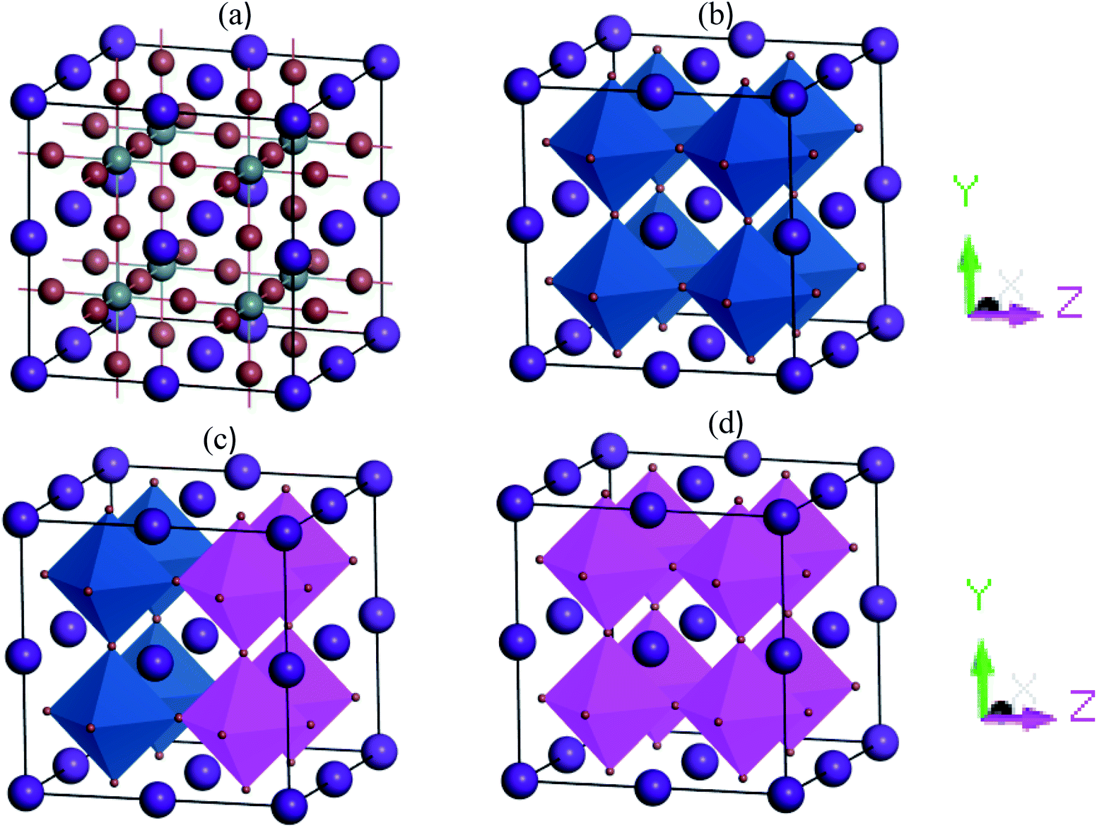 | ||
| Fig. 1 2 × 2 × 2 supercell structures of (a) CsSnI3 (balk-and-stick) (b) CsSnI3 (polyhedral), (c) CsSn0.5Cu0.5I3, and (d) CsCuI3. | ||
Phase stability is more essential for materials. To be stable, the materials have to fulfill some special criteria. Firstly, for mechanical stability, a material must have full-filled elastic moduli conditions. The second one is phase stability. In a single halide perovskites material, phase stability is calculated by the tolerance equation.35
 | (1) |
Xiao Feng et al. reported that the CsSnI3 sample has poor stability and can't be suitable for devices.24 Notably, the Cu-doped CsSnI3 samples have increased phase stability. To gain phase stability, we have employed the Shannon ionic radius. Finally, we concluded that the Cu-doped CsSnI3 samples may have potential applications for device purpose.
The formation enthalpy is calculated by the following equations36,37
For an un-doped system,
 | (2) |
 | (3) |
| Samples | a0 (Å) | V0 (Å3) | ΔHf | t | ||
|---|---|---|---|---|---|---|
| This study | Ref. | This study | Ref. | This study | This study | |
| a Ref. 38.b Ref. 8.c Ref. 39. | ||||||
| CsSnI3 | 6.27 | 6.24a, 6.2c | 247.44 | 238.9b | −2.03 | 0.99 |
| CsSn0.875Cu0.125I3 | 6.24 | — | 243.37 | — | −7.24 | — |
| CsSn0.25Cu0.75I3 | 6.20 | — | 238.80 | — | −7.28 | — |
| CsSn0.5Cu0.5I3 | 5.98 | — | 213.91 | — | −1.00 | — |
| CsCuI3 | 5.68 | — | 183.97 | — | −2.52 | 1.02 |
3.2. Electronic properties
To see the electronic behaviors of pure and Cu-doped CsSnI3 perovskite, we have simulated the electronic band energy along with high symmetry points. The calculated band energy structures are shown in Fig. 2(a–f). The simulated band structures of the pure CsSnI3 have direct band gap of 0.44 eV, where the maximum valence band and minimum conduction bands are staying at similar k-points. The single cell band gap has small difference from the supercell structure (eight times) band gap. Note that band gap values for unit cell are 0.442 eV and 2 × 2 × 2 supercells of CsSnI3 for 0.445, which suggesting the good convergence of the orbital fluctuations.20 It is seen that the simulated band gap value underestimates the experimentally calculated band gap values of 1.27 eV.40 Several researchers reported that the hybrid potential HSC (Heyd–Scuseria–Ernzerhof) methods are perfect for exact band gap measurements, although this potential is not fit for estimate samples.13,19 The experimental calculated band gap value differs from the theoretical band gap due to the limitations of GGA method. However, our work focuses only on the reduction of electrical band gap of Cu-doped CsSnI3 and ignores the band gap error for the GGA method. The present band gap energy values are good in agreement with other publication.40 It is noteworthy that Cu-doped CsSnI3 samples appear in intermediate states.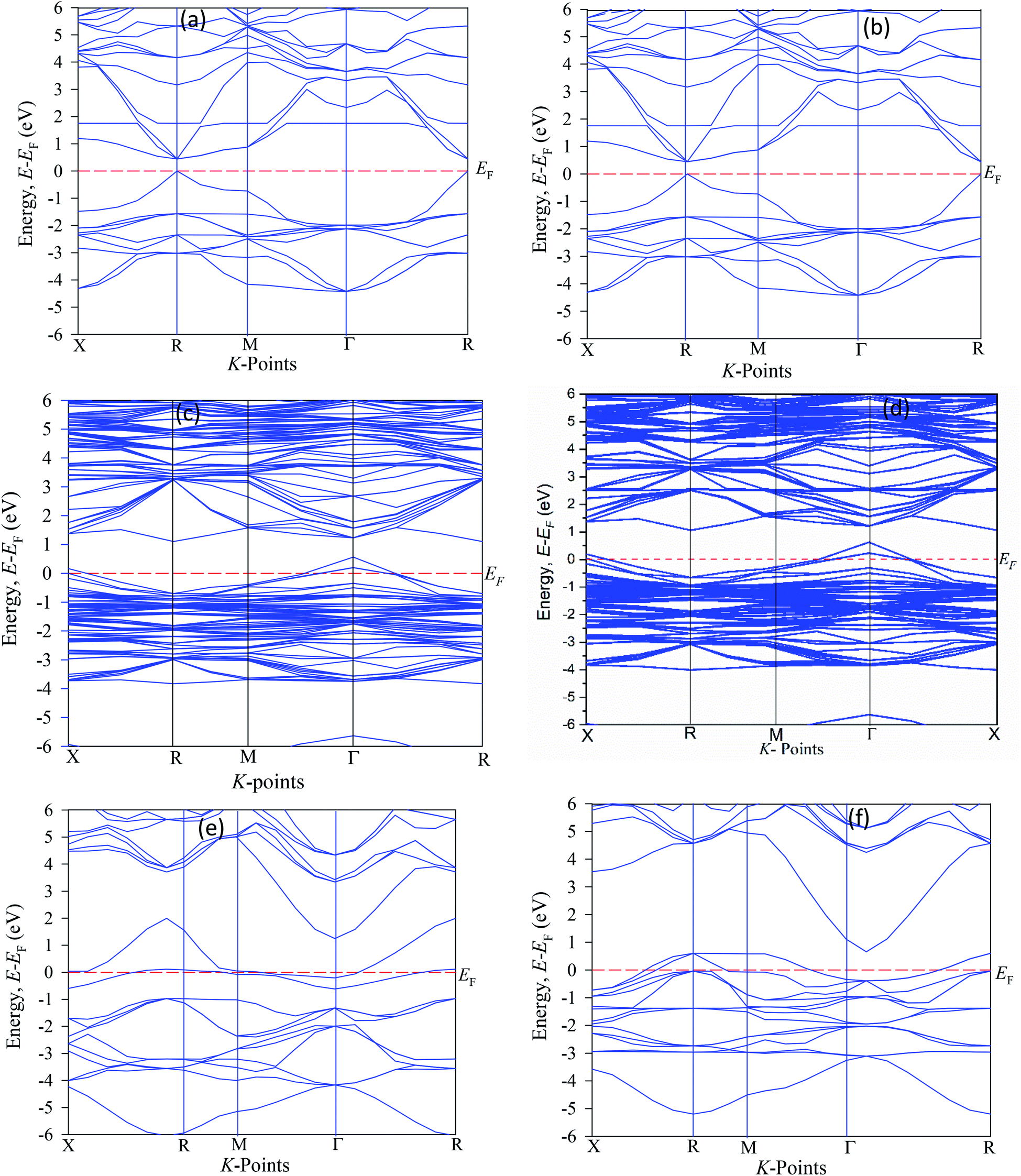 | ||
| Fig. 2 The band structure diagram of CsSnI3 (a) pure unit cell, (b) pure supercell, (c) CsSn0.875 Cu0.125I3 (d) CsSn0.75 Cu0.25I3, (e) CsSn0.5 Cu0.5I3, and (f) Cs CuI3. | ||
The valence energy states are expanded into the higher energy region due to the valence band into the Fermi level can cross the transition of electrons from the valence band to the conduction band. Here, shifting of the Fermi level into the valence band can be described as the negative Burstein shift. However, band gap energy is calculated by the maximum valence band gap to the minimum conduction band gaps. It can be seen from Cu-doped CsSnI3 samples, the valence band (VB) maximum and conduction band (CB) minimum are lying at dissimilar k-points which is indicating the samples have indirect band gap natures. The indirect band gap nature samples have strong absorption and long charge carrier lifetime rather than direct semiconductor samples. The indirect band figure indicates that the electron cannot move to the highest-energy states in the valence band to the conduction band, without in change k-points momentum energy. Generally, the indirect nature semiconductors are a promising candidate for photovoltaic device applications. The calculated band gap values are tabulated in Table 2 along with previously published theoretical and experimental results. The calculated band structure suggests that the pattern of the band gap is affected by the Cu-doping concentrations. The total density of states (TDOS) and partial density of states (PDOS) of pure and Cu-doped CsSnI3 samples are presented in Fig. 3(a–f). As shown in the partial density of states figure the valence band is mostly composed of Cu-3d and I-6s orbital with a small contribution of Cs-6s and Cs-3p states. The high energy band is mainly dominated by Cu-3d orbital with a small contribution of Cs-6s and Cs-5p electrons. The band structure identifies that the difference between valences band maximum to the conduction band minimum in a sample. The TDOS shape of Cu-doped CsSnI3 becomes broader than that of pure CsSnI3, which indicates that the electronic non-locality is more because of the reduction of crystal symmetry.41 The conduction band energy is mostly attributed to the Cu atom due to CB shifts towards the lowest energy states. A flat peak is seen in the conduction band because Cu-3d states are generated by new dopants energy states. It is observed from Cu-doped CsSnI3 samples, the impurity energy states appear in the partial density of states. This intermediate state appears electronic band structure, which is essential for electrons transition between conduction bands to valence bands.
| Samples | Types of band gap | Present work | Band gap value, Eg (eV) | |
|---|---|---|---|---|
| Exp. ref. | Theo. ref. | |||
| a Ref. 34.b Ref. 28.c Ref. 42. | ||||
| CsSnI3 (unit cell) | Direct | 0.442 | 1.27a | 0.30b, 0.59b, 0.38c |
| CsSnI3 (supercell) | Direct | 0.445 | — | — |
| CsSn0.875Cu0.125I3 | Indirect | 0.59 | — | — |
| CsSn0.25Cu0.75I3 | Indirect | 0.48 | — | — |
| CsSn0.5Cu0.5I3 | Indirect | 0.42 | — | — |
| CsSnCuI3 | Indirect | 0.29 | — | — |
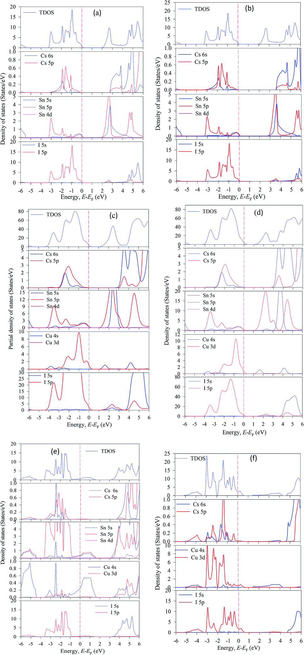 | ||
| Fig. 3 The total and partial density of states of CsSnI3, (a) pure unit cell, (b) pure supercell, (c) CsSn0.875 Cu0.125I3, (d) CsSn0.75 Cu0.25I3, (e) CsSn0.5 Cu0.5I3 and (f) Cs CuI3. | ||
 | (4) |
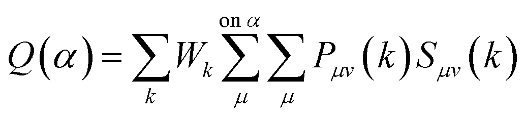
The overlap population between two atoms α and β can be expressed using the following equation44
 | (5) |
Noticeably, the Mulliken effective charges of the individual Cs, Sn, I, and Cu atoms are found to be reasonably smaller than their formal ionic charges, which are +1, +4, −1, and +2, respectively.
To see the difference between Mulliken effective charge and formal ionic radius, we have applied the Shannon ionic radius. The difference between Mulliken effective charges and formal ionic radius indicates that the CsSn1−xCuxI3 (x = 0, 0.125, 0.25, 0.5, 1) samples have mixed ionic and covalent bonds (Table 3).
| Samples | Species | Effective valence charge (e) | Bonds | Bond population | Bond length (Å) |
|---|---|---|---|---|---|
| CsSnI3 | Cs | 0.53 | Sn–I | 0.07 | 3.139 |
| Sn | 0.32 | ||||
| I | −0.28 | ||||
| CsSn0.875Cu0.125I3 | Cs | 0.52 | Cu–I | 0.08 | 3.02 |
| Sn | 0.32 | Sn–I | 0.02 | 3.11 | |
| I | −0.26 | Cs–I | 0.33 | 7.64 | |
| Cu | −0.36 | ||||
| CsSn0.75Cu0.25I3 | Cs | 0.51 | Cu–I | 0.06 | 2.96 |
| Sn | 0.31 | Sn–I | 0.01 | 3.09 | |
| I | −0.26 | Cu–Cs | 0.04 | 7.59 | |
| Cu | −0.42 | ||||
| CsSn0.5Cu0.5I3 | Cs | −0.13 | Cu–I | 0.25 | 2.87 |
| Sn | 0.30 | Sn–I | 0.08 | 3.199 | |
| I | 0.21 | Cu–Cs | 0.28 | 3.199 | |
| Cu | −0.49 | ||||
| CsCuI3 | Cs | 0.32 | Cu–I | 0.23 | 2.843 |
| Cu | −0.65 | Cu–Cs | 0.64 | 4.92 | |
| I | 0.11 |
The effective valence charge is reduced with Cu-doping concentrations. The level of covalence Cu-doped CsSnI3 reduced due to the effect of on-site Coulomb interaction. The positive value of bond population refers to the high degree of covalence, whereas the small bond population identifies a high degree of ionicity in the covalence bond.45 Moreover, the simulated bond populations of Cu–I are found to be higher than the Sn–I. The bond length is decreased in pristine CsSnI3 compared to Cu-doped CsSnI3 due to ionic radius mismatch between Sn and Cu atoms.
To see the charge distribution and bonding nature of pristine and Cu-doped CsSnI3, we analyzed charge density distribution and presented it in Fig. 4(a–e). Spherical shape charge distribution exists in the pure and Cu-doped CsSnI3. Sn and Cu atoms are bonded covalently with the I atom. The electron clouds around Sn, Cu, and I atoms are distorted towards, which indicating the covalent bond natures. Fig. 4 shows the almost similar charge distribution and bonding character of pure and Cu-doped CsSnI3 perovskites.
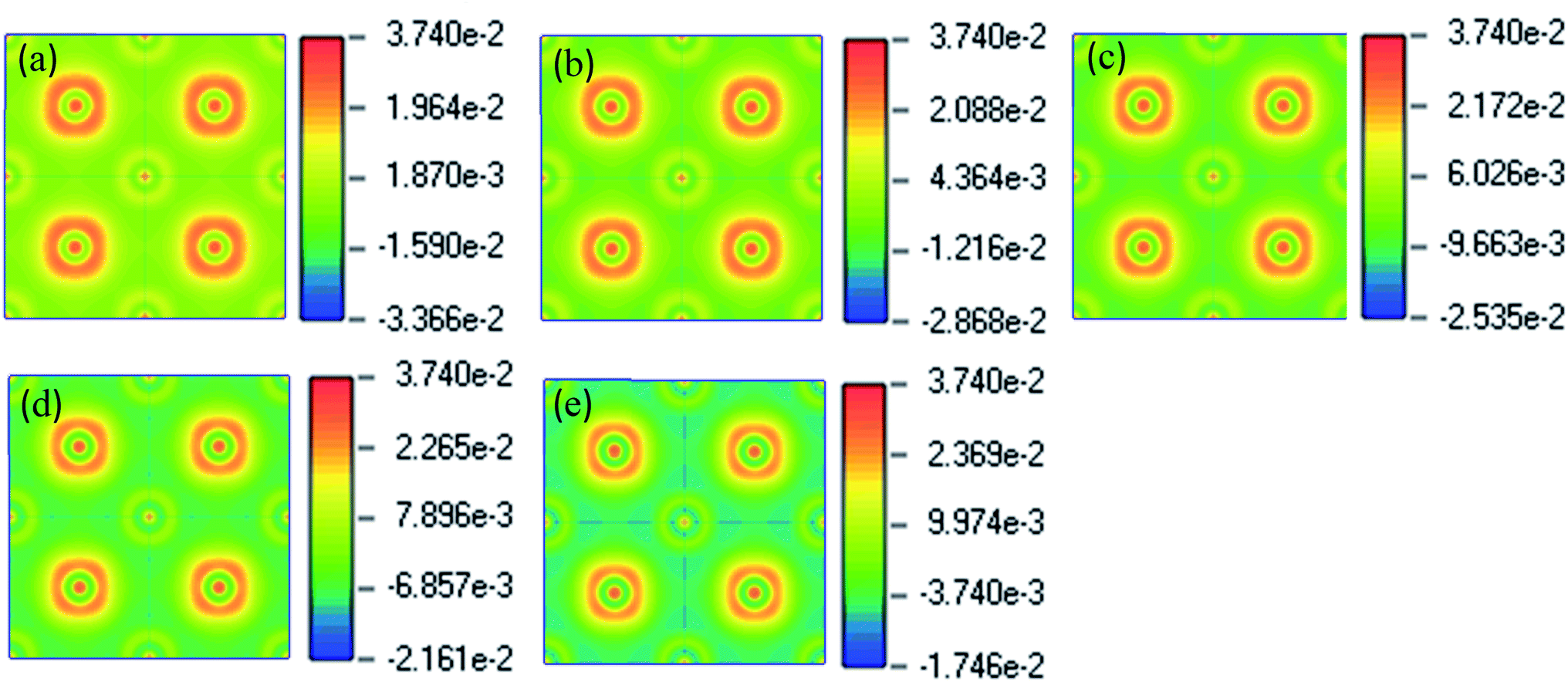 | ||
| Fig. 4 The electric charge density (a) CsSnI3, (b) CsSn0.87.5Cu0.125I3, (c) CsSn0.75Cu0.25I3, (d) CsSn0.5Cu0.5I3 and (e) CsCuI3. | ||
Photo-catalytic is an essential parameter to identify the device efficiency of optoelectronic and photovoltaic applications. Tin-based halides CsSnI3 have more response to photo-catalytic materials. Cu-doped CsSnI3 samples, photo-catalytic activity tends to increase in comparation to pristine CsSnI3. Charge carrier mobility transition samples have more photocatalytic activities efficiency. In this paper, we found that the CsSnI3 has a direct electrical band gap of 0.44 eV and Cu-doped CsSnI3 the sample is transferred from direct band gap energy into indirect. The indirect electrical band gap of CsSnI3 samples shows a long lifetime of photo-excited electrons and holes comparsion than direct electrical band gap semiconductors due to the direct apartness of photogenerated electrons from the CB to the VB of a semiconductor is not possible. The excited electrons from the valence band (VB) are injected into the conduction band (CB), which changes the gap energy in Cu-doped CsSnI3 samples. The band energy alignment of photocatalytic is shown in Fig. 5. It gives the influence of the separation of photo-generated electron–hole pairs, as well as favors in migration of photo-excited carriers and processing photo-catalysis. Cu-doped CsSnI3 samples introduction of new dopant energy levels that effectively changes the band gap energy of the photo-catalyst. This work would be suitable for optoelectronic and photovoltaic device applications.
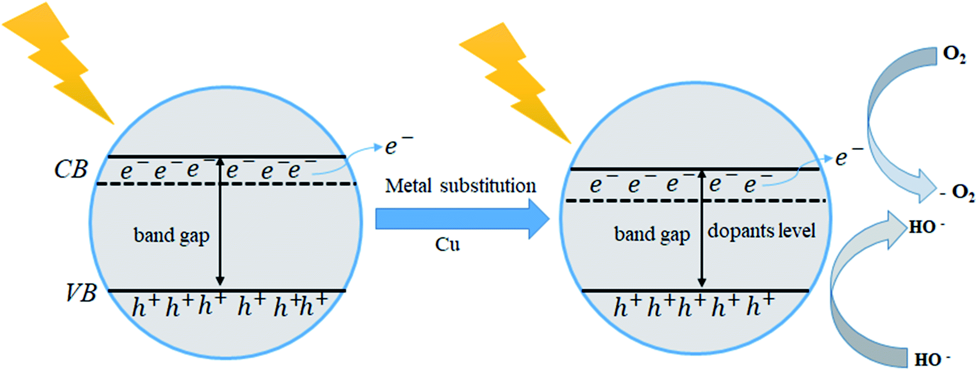 | ||
| Fig. 5 Schematic plot of band energy alignment of the photo catalytic of CsSnI3. | ||
3.3. Mechanical properties
The three independent elastic moduli for pure and Cu-doped CsSnI3 perovskites are simulated by the finite strain theory.43,46 The single and polycrystalline elastic properties are simulated via CASTEP code material studio 8.0 and tabularized in Tables 4 and 5. The simulated polycrystalline properties for CsSnI3 are good to coincide with the previously published paper.34 For cubic symmetry criteria, the simulated elastic modulus of pure and Cu-doped CsSnI3 compound should satisfy the following conditions:44,47 C11 + 2C12 > 0, C44 > 0 and C11 − C44 > 0. The simulated elastic modulus for pure and Cu-doped CsSnI3 full filed the mechanical stability criteria, which indicating that pristine and Cu-doped CsSnI3 samples are mechanically stable. The quantity C12–C44, is defined as Cauchy pressure,45,48 which identifies the brittle/ductile nature of a sample. The simulated Cauchy pressure is positive values, which ensures that the pristine and Cu-doped CsSnI3 samples are ductile natures (Fig. 6).| Samples | C11 | C12 | C44 | C12–C44 | Reference |
|---|---|---|---|---|---|
| CsSnI3 | 33.59 | 16.79 | 8.65 | 8.14 | — |
| CsSn0.875Cu0.125I3 | 22.74 | 6.68 | 4.47 | 2.22 | — |
| CsSn0.25Cu0.75I3 | 19.02 | 5.89 | 3.97 | 1.92 | — |
| CsSn0.5Cu0.5I3 | 28.23 | 12.24 | 8.88 | 4.00 | — |
| CsCuI3 | 33.59 | 16.79 | 8.68 | 8.11 | — |
| Samples | B (GPa) | G (GPa) | Y (GPa) | B/G | v | Reference |
|---|---|---|---|---|---|---|
| 16.56 | 9.03 | 22.92 | 1.83 | 0.26 | 34 | |
| CsSnI3 | 15.57 | 8.78 | 22.19 | 1.77 | 0.26 | — |
| CsSn0.875Cu0.125I3 | 12.04 | 5.90 | 15.22 | 2.04 | 0.28 | — |
| CsSn0.75Cu0.25I3 | 14.03 | 4.82 | 13.62 | 2.90 | 0.27 | — |
| CsSn0.5Cu0.5I3 | 17.57 | 8.52 | 22.02 | 2.02 | 0.30 | — |
| CsCuI3 | 22.39 | 8.55 | 22.75 | 2.61 | 0.33 | — |
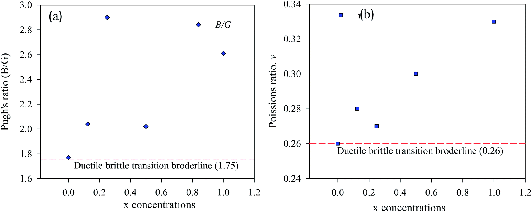 | ||
| Fig. 6 The ductile and brittle behavior (a) Pugh's ratio, (b) Poisons ratio of CsSn1−xCuxI3, (x = 0, 0.125, 0.25, 0.5, 1). | ||
The evaluated bulk modulus, shear modulus, Young's modulus, Pugh's ratio, and Poisson's ratio of the pure and Cu-doped CsSnI3 samples are presented in Table 5. The bulk modulus values are identified that pure and Cu-doped CsSnI3 samples are flexible and soft. Therefore, these metal halide perovskites can easily be made into a suitable thin film for optoelectronic applications especially for solar cells. Bulk modulus to shear modulus ratio (B/G) is called Pugh's ratio and Poisson's ratio both can identify the ductility/brittleness nature of a material.49,50 The critical value of Pugh's and Poisons distinguish the brittle materials from ductile ones. If the Pugh's (0.26) and Poisson's ratio (1.75) values are higher than critical values, then the sample is said to be in ductile types, otherwise, it is brittle types. The ductile nature is tended to reduce with Cu-doping concentrations. Cauchy pressure predicted that pristine and Cu substitution doped CsSnI3 samples are ductile in nature. It can be seen from single and polycrystalline; elastic properties (Tables 4 and 5) are changed with Cu-doping concentrations. Notable, the single elastic properties of Cu-doped CsSnI3 samples are nearly similar with pristine CsSnI3 sample. The mechanical stability and ductility natures imply that the pure and Cu-doped CsSnI3 samples are perfect for the thin films industry.
3.4. Optical properties
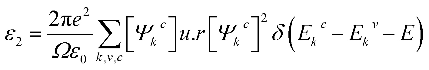
To understand the optical behaviors, we simulated optical absorption (α), conductivity (σ), and dielectric constant (ε) for pristine and Cu-doped CsSnI3 samples. The complex dielectric function is given by the following equations.51| ε(ω) = ε1(ω) + iε2(ω) = N2 | (6) |
The complex dielectric function is expressed by the following equations52
 | (7) |
To see optical nature, we used photon energy, E, 0 to 20 eV. In this manuscript, the Gaussian smearing of 0.5 eV was used for all simulations. The optical properties calculation were taken in the {100} plane orientation. A scissor value is applied of 0.68 eV, which is the disparity between experimental and theoretical band gap energy.
The simulated absorption spectra of pristine and Cu-doped CsSnI3 are presented in Fig. 7(a and b). The optical absorption coefficient α(ω) gives the information about the amount of light entrance with a particular wavelength into solid materials.28
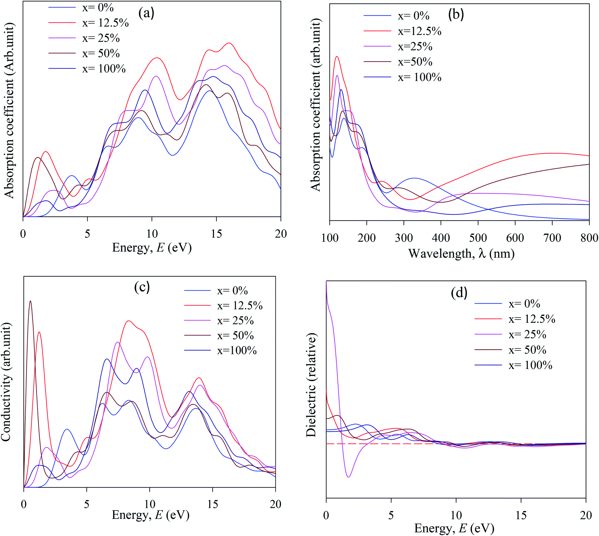 | ||
| Fig. 7 The simulated optical properties (a) absorbance vs. energy, (b) absorbance vs. wavelength, (c) optical conductivity, and (d) imaginary part of dielectric function of CsSn1−xCuxI3, (x = 0, 0.125, 0.25, 0.5, 1). | ||
It also gives information about solar spectrum energy which is most important for devices application, especially for solar cells. First, absorption peak is more essential for device applications. The absorption spectra were taken in the range of 100–800 nm to investigate the optical behavior in the UV-vis. and visible wave length (λ) range. Accordingly, the absorption spectra are shifted to the lower energy region (redshift) compared to pure and Cu-doped CsSnI3. The absorption spectra confirmed that Cu has a large influence on the band gap energy and finally decreased the band gap. The absorption band is shifted towards the lower energy region due to Sn and Cu ions created defect energy of Cu 3d and Sn 4d orbitals.
Stronger optical absorption spectra identify increase photovoltaic efficiency. Hence the band gap energy transferred towards the visible region and the maximum absorption peak occurred in the UV region, which indicates that the pure and Cu-doped CsSnI3 samples are potential candidates for the optoelectronics industry. The absorption spectra threshold energy is significantly higher than the simulated band gap, which is indicating that the CsSnI3 sample has direct band gap nature and reverses at Cu-doped CsSnI3 samples. The first absorption peak stay at 1.0–4.5 eV energy regions, which demonstrated that pure and Cu-doped CsSnI3 samples are perfect for photoelectric device applications. The simulated optical conductivity (σ) are presented in Fig. 7(c). The optical conductivity is an essential parameter for identifying how the amount of electromagnetic wave response in a substance. Moreover, the optical conductivity (σ) refers to the number of photons that pass through the substance. The optical conductivity and absorption spectra have a similar structure, as presented in Fig. 7(a–c), due to the escape of electron and photon from the valence band to the conduction band when it absorbs energy. The optical conductivity of Cu-doped CsSnI3 occurs at lower energy compared with pristine CsSnI3. Optical conductivity at low energy of Cu-doped CsSnI3 perovskites makes them potential candidate materials for applications in optoelectronic especially solar cells devices. Optical conductivity results confirm that Cu-doped CsSnI3 samples have a low band gap compared with their pristine CsSnI3. The dielectric function gives information about the amount of electromagnetic radiation response in a solid substance.53 The imaginary part of the dielectric function (ε2) is similar to electron excitation. Notable, the first peak of the imaginary part of the dielectric function (ε2) occurs at <1.5 eV, at Cu-doped CsSnI3 samples, which indicates that the intra-band transition has occurred and vice versa at pure CsSnI3. The overall optical properties recommend that Cu-doped CsSnI3 is perfect for optoelectronic especially solar cell applications.
4. Conclusions
In this work, we have applied the density functional theory (DFT) simulations to calculate structural, electronic, mechanical, and optical properties of pure and Cu-doped CsSnI3 samples. The structural parameters lattice constants a, and cell volumes, V are well-matched with previously published work. The simulated band structure reveals that the pure CsSnI3 sample has a direct band gap nature semiconductor. In the case of Cu-doped CsSnI3 samples, the band gap energy transferred towards direct to indirect. The Pugh's and Poisson's ratio refers that the pure and Cu-doped CsSnI3 samples are to be fabricated easily in the thin films industry. The absorption edge is transferred to the lower energy regions with Cu-doping concentrations. The dielectric properties manifested that inter-band transferred towards the intra-band due to changes of the band gap energy at Cu-doped samples. A combined evaluation of the structural, electronic, mechanical, and optical properties recommend that eco-friendly CsSn1−xCuxI3 (x = 0, 0.125, 0.25, 0.5, 1) perovskite is a suitable candidate materials for photovoltaic and optoelectronic device applications.Author contributions
M. N. Islam: conceptualization, data curation, investigation, methodology, software, formal analysis, writing-original draft, J. Podder: supervision, data curation, formal analysis, review and editing, M. L. Ali: formal analysis, software.Conflicts of interest
The authors declare no conflict of interest.Acknowledgements
The authors are thankful to the spray pyrolysis and the crystal growth laboratory of the Department of Physics, Bangladesh University of Engineering and Technology, Dhaka, Bangladesh for performing this theoretical research using the laboratory computer facilities and package.References
- A. Mahsa, A. Boochani and M. Hantezadeh, Electronic, optical and elastic properties of cubic perovskite CsPbI3: Using first principles study, Optik, 2016, 127, 11433–11443 CrossRef.
- B. V. Lotsch, New light on an old story: perovskites go solar, Angew. Chem., Int. Ed., 2014, 53, 635–637 CrossRef CAS PubMed.
- S. Kazim, M. K. Nazeeruddin, M. Grätzel and S. Ahmad, Perovskite as light harvester: a game changer in photovoltaics, Angew. Chem., Int. Ed., 2014, 53, 2812–2824 CrossRef CAS PubMed.
- N. J. Jeon, J. H. Noh, W. S. Yang, Y. C. Kim, S. Ryu, J. Seo and S. I. Seok, Compositional engineering of perovskite materials for high-performance solar cells, Nature, 2015, 517, 476–480 CrossRef CAS PubMed.
- J. Shi, Y. Luo, H. Wei, J. Luo, J. Dong, J. Lv and Q. Meng, Modified two-step deposition method for high-efficiency TiO2/CH3NH3PbI3 heterojunction solar cells, ACS Appl. Mater. Interfaces, 2014, 12, 9711–9718 CrossRef PubMed.
- F. Hao, C. C. Stoumpos, D. H. Cao, R. P. Chang and M. G. Kanatzidis, Lead-free solid-state organic–inorganic halide perovskite solar cells, Nat. Photonics, 2014, 8, 489–494 CrossRef CAS.
- I. Chung, J. H. Song, J. Im, J. Androulakis, C. D. Malliakas, H. Li, A. J. Freeman, J. T. Kenney and M. G. Kanatzidis, CsSnI3: Semiconductor or Metal? High Electrical Conductivity and Strong Near-Infrared Photoluminescence from a Single Material. High Hole Mobility and Phase-Transitions, J. Am. Chem. Soc., 2012, 134, 8579–8587 CrossRef CAS PubMed.
- K. Yamada, S. Funabiki, H. Horimoto, T. Matsui, T. Okuda and S. Ichiba, Structural Phase Transition of Polymorphs of CsSnI3 by Means of Rietveld Analysis of the X-Ray Diffraction, Chem. Lett., 1991, 20, 801–804 CrossRef.
- D. E. Scaife, P. F. Weller and W. G. Fisher, Crystal preparation and properties cesium tin trihalides, J. Solid State Chem., 1974, 9, 308–314 CrossRef CAS.
- W. S. Yang, J. H. Noh, N. J. Jeon, Y. C. Kim, S. Ryu, J. Seo and S. I. Seok, High-performance photovoltaic perovskite layers fabricated through intramolecular exchange, Science, 2015, 348, 1234–1237 CrossRef CAS PubMed.
- I. Borriello, G. Cantele and D. Ninno, Ab initio investigation of hybrid organic–inorganic perovskites based on tin halides, Phys. Rev. B: Condens. Matter Mater. Phys., 2008, 77, 235214 CrossRef.
- M. Roknuzzaman, K. Ostrikov, H. Wang, A. Du and T. Tesfamichael, Towards lead free perovskite photovoltaic and optoelectronic by ab-initio simulations, Sci. Rep., 2017, 7, 14025 CrossRef PubMed.
- H. Chen, L. Zhou, Z. Fang, S. Wang, T. Yang, L. Zhu, X. Hou, H. Wang and Z. L. Wang, Piezoelectric Nanogenerator Based on In Situ Growth All-Inorganic CsPbBr3 Perovskite Nanocrystals in PVDF Fibers with Long-Term Stability, Adv. Funct. Mater., 2021, 31, 2011073 CrossRef CAS.
- Z. Yong, S. Guo, J. Ma, J. Zhang, Z. Li, Y. Chen, B. Zhang, Y. Zhou, J. Shu, J. G. Zheng, O. Bakr and H. Sun, Doping-Enhanced Short-Range Order of Perovskite Nano crystals for Near-Unity Violet Luminescence Quantum Yield, J. Am. Chem. Soc., 2018, 140, 9942–9951 CrossRef CAS PubMed.
- B. Yang, J. Chen, F. Hong, X. Mao, K. Zheng, S. Yang, Y. Li, T. Pullerits, W. Deng and K. Han, Lead-Free, Air-Stable All-Inorganic Cesium Bismuth Halide Perovskite Nanocrystals, Angew. Chem., Int. Ed., 2017, 56, 12471–12475 CrossRef CAS PubMed.
- Y. Fu, H. Zhu, A. Schrader, D. Liang, Q. Ding, P. Joshi, L. Hwang, X. Zhu and S. Jin, Nanowire Lasers of Formamidinium Lead Halide Perovskites and Their Stabilized Alloys with Improved Stability, Nano Lett., 2016, 16, 1000–1008 CrossRef CAS PubMed.
- T. Yang, Y. Zheng, K. Chou and X. Hou, Tunable fabrication of single-crystalline CsPbI3 nanobelts and their application as photodetectors, Int. J. Miner., Metall. Mater., 2021, 28, 1030–1037 CrossRef CAS.
- T. Yang, Y. Zheng, Z. Du, W. Liu, Z. Yang, F. Gao, L. Wang, K. Chou, X. Hou and W. Yang, Superior Photodetectors Based on All-Inorganic Perovskite CsPbI3 Nanorods with Ultrafast Response and High Stability, ACS Nano, 2018, 12, 1611–1617 CrossRef CAS PubMed.
- T. Meiqian, C. F. J. Lau, H. Lin and Z. Wang, Advances in Phase Stability of Cesium Lead Halide Perovskites, Solar RRL, 2020, 12, 2000495 Search PubMed.
- Q. Liu, J. Yin, B. Zhang, J. K. Chen, O. M. Bakr and H. T. Sun, Metal-doped lead halide perovskites: synthesis, properties, and optoelectronic applications, J. Am. Chem. Soc., 2020, 143, 5470–5480 CrossRef PubMed.
- J. H. Noh, S. H. Im, J. H. Heo, T. N. Mandal and S. I. Seok, Chemical management for colorful, efficient, and stable inorganic–organic hybrid nanostructured solar cells, Nano Lett., 2013, 13, 1764–1769 CrossRef CAS PubMed.
- E. Edri, S. Kirmayer, M. Kulbak, G. Hodes and D. Cahen, Chloride inclusion and hole transport material doping to improve methyl ammonium lead bromide perovskite-based high open-circuit voltage solar cells, J. Phys. Chem. Lett., 2014, 5, 429–433 CrossRef CAS PubMed.
- X. Qiu, B. Cao, S. Yuan, X. Chen, Z. Qiu, Y. Jiang, Q. Ye, H. Wang, H. Zeng, J. Liu and M. G. Kanatzidis, From unstable CsSnI3 to air stable Cs2SnI6: A lead free perovskite for solar cell light absorber with band gap 1.48 eV and high absorption coefficient, Solar Ener. Mater. Solar Cells, 2017, 159, 227–234 CrossRef CAS.
- L. Borriello, G. Cantele and D. Ninno, Ab initio investigation of hybrid organic–inorganic perovskites based on tin halides, Phys. Rev. B: Condens. Matter Mater. Phys., 2008, 77, 235214 CrossRef.
- L. Y. Huang and W. R. Lambrecht, Electronic band structure, phonons, and exciton binding energies of halide perovskites CsSnCl3, CsSnBr3, and CsSnI3, Phys. Rev. B: Condens. Matter Mater. Phys., 2013, 88, 165203 CrossRef.
- M. Z. Rahaman and A. K. M. A. Hossain, effect of metal doping on the visible light absorption, electronic structure and mechanical properties of non-toxic metal halide CsGeCl3, RSC Adv., 2018, 8, 33010 RSC.
- E. Burstein, Anomalous optical absorption limit in InSb, Phys. Rev., 1954, 93, 632 CrossRef CAS.
- M. N. Islam, M. A. Hadi and J. Podder, Influence of Ni doping in a lead halide and lead free halide perovskites for optoelectronic applications, AIP Adv, 2019, 9, 125321 CrossRef.
- M. A. Hadi, M. N. Islam and M. H. Babu, Cubic perovskite Pb (Mg1/3Nb2/3) O3: A damage tolerant, machinable, and thermal barrier, Z. Naturforsch, 2019, 74, 71–81 CrossRef CAS.
- M. N. Islam, J. Podder, T. Saha and P. Rani, Semiconductor to metallic transition under induced pressure in Cs2AgBiBr6 double halide perovskite: a theoretical DFT study for photovoltaic and optoelectronic applications, RSC Adv., 2021, 11, 24001 RSC.
- M. A. Hadi, R. V. Vouk and A. Chroneos, Physical properties of the recently discovered Zr2 (Al1− x Bix) C MAX phases, J. Mater. Sci. Mater. Electron., 2017, 27, 11925 CrossRef.
- M. N. Islam and J. Podder, The role of Al and Co co-doping on the band gap tuning of TiO2 thin films for applications in photovoltaic and optoelectronic devices, Matt. Sci. Proc., 2021, 121, 105419 CAS.
- M. Babu, C. B. Dev, J. Podder and N. Islam, Influence of Fe2+/Fe3+ ions in tuning the optical band gap of SnO2 nanoparticles synthesized by TSP method: Surface morphology, structural and optical studies, Matt. Sci. Proc., 2019, 89, 223 Search PubMed.
- C. Li, X. Lu, W. Ding, L. Feng, Y. Gao and Z. Guo, Formability of ABX3 (X = f, cl, br,i) halide perovskites, Acta Crystallogr., 2008, 64, 702 CAS.
- M. Shakil, A. Akram, I. Zeba, R. Ahmad, S. S. A. Gillani and M. A. Gadhi, Effect of mixed halide contents on structural, electronic, optical and elastic properties of CsSnI3− xBrx for solar cell applications: first-principles study, Mat. Res. Exp., 2020, 7, 025513 CrossRef CAS.
- E. L. d. Silva, J. M. Skelton, S. C. Parker and A. Walsh, Phase stability and transformations in the halide perovskite CsSnI3, Phys. Rev. B: Condens. Matter Mater. Phys., 2015, 91, 144107 CrossRef.
- Y. Pan, Y. Lin, G. Liu and J. Zhang, Influence of transition metal on the mechanical and thermodynamic properties of IrAl thermal barrier coating, Vacuum, 2020, 174, 109203 CrossRef CAS.
- M. J. Jurow, T. Morgenstern, C. Eisler, J. Kang, E. Penzo, M. Q. Do and C. J. Tassone, Manipulating the transition dipole moment of CsPbBr3 perovskite nanocrystals for superior optical properties, Nano Lett., 2019, 19, 2489–2496 CrossRef CAS PubMed.
- J. Heyd, J. E. Peralta, G. E. Scuseria and R. L. Martin, Energy band gaps and lattice parameters evaluated with the Heyd-ScuseriaErnzerhof screened hybrid functional, J. Chem. Phys., 2005, 123, 174101 CrossRef PubMed.
- J. Heyd, J. E. Peralta, G. E. Scuseria and R. L. Martin, Energy band gaps and lattice parameters evaluated with the Heyd-Scuseria Ernzerhof screened hybrid functional, J. Chem. Phys., 2005, 123, 174101 CrossRef PubMed.
- B. Saruhan, A. Yüce, Y. Gönüllü and K. Kelm, Effect of Al doping on NO2 gas sensing of TiO2 at elevated temperatures, Sens. Actuators, B, 2013, 187, 586–597 CrossRef CAS.
- Z. Ma, F. Li, G. Qi, L. Wang, C. Liu, K. Wang and B. Zou, Structural stability and optical properties of two-dimensional perovskite-like CsPb2Br5 microplates in response to pressure, Nanoscale, 2009, 11, 820–825 RSC.
- R. S. Mulliken, Electronic population analysis on LCAO-MO molecular wave functions, I, J Chem Phys, 1955, 23, 1833–1840 CrossRef CAS.
- M. D. Segall, R. Shah, C. J. Pickard and M. C. Payne, Population analysis of plane-wave electronic structure calculations of bulk materials, Phys. Rev. B: Condens. Matter Mater. Phys., 1996, 54, 16317 CrossRef CAS PubMed.
- R. Zilah R, M. K. Yaakob, Z. Mohamed and A. K. Yahya, Effects of onsite Coulomb interaction (U) on the structural and electronic properties of half-metallic ferromagnetic orthorhombic Pr0.75Na0.25 MnO3 manganite: a LDA+U calculation and experimental study, Mater. Res. Express, 2017, 4, 066103 CrossRef.
- D. Liyuan, S. Shijing, D. Zeyu, L. Wei, W. Fengxia, Q. Yajun, L. Yanchun, L. Xiaodong, L. Peixiang and U. Ramanurty, Elastic properties and thermal expansion of lead-free halide double perovskite Cs2AgBiBr6, Comput. Mater. Sci., 2018, 141, 49–58 CrossRef.
- M. A. Hadi, R. V. Vouk and A. Chroneos, Physical properties of the recently discovered Zr2 (Al1−xBix) C MAX phases, J. Mater. Sci. Mater. Electron., 2017, 27, 11925 CrossRef.
- Y. Weinan, N. Guangda, X. Yeming, W. Haodi, W. Huamin, Y. Hang, L. Peng, L. Wenzhe and F. Jiandong, In Situ Regulating the Order–Disorder Phase Transition in Cs2AgBiBr6 Single Crystal toward the Application in an X-Ray Detector, Adv. Funct. Mater., 2019, 29, 1900234 CrossRef.
- L. Chunfeng, Z. Shuai, L. Jingting and F. Ping, First-principles study of anion diffusion in lead-free halide double perovskites, Phys. Chem. Chem. Phys., 2018, 20, 24344 Search PubMed.
- Z. Jun, X. Zhiguo, M. S. Maxim, Z. Xiuwen, P. Dongsheng and L. Quanlin, Composition design, optical gap and stability investigations of lead-free halide double perovskite Cs2 AgInCl6, J. Mater. Chem. A, 2017, 5, 15037 Search PubMed.
- K. O. Obodo, G. Gebreyesus, C. N. M. Ouma, J. T. Obod, S. O. Ezeonu, D. P. Raif and B. Bouhafs, Controlling the electronic and optical properties of HfS2 mono-layers via lanthanide substitutional doping: a DFT+ U study, RSC Adv., 2020, 10, 15670 RSC.
- M. A. Hadi, Md Roknuzzaman, M. T. Nasir, U. Monira, S. H. Naqib, A. Chroneos, A. K. M. A. Islam, J. A. Alarco and Kostya Ostrikov, Effects of Al substitution by Si in Ti3AlC2 nanolaminate, Sci. Repor., 2021, 11, 3410 CrossRef CAS PubMed.
- H. Ayatullahah, G. Murtaza, S. Muhammad, S. Naeem, M. N. Khalid and A. Manzar, Physical properties of CsSnM3 (M ¼ Cl, Br, I): A first principle study, Acta Phys. Pol., A, 2013, 124, 102–107 CrossRef.
| This journal is © The Royal Society of Chemistry 2021 |