
 Open Access Article
 This Open Access Article is licensed under a Creative Commons Attribution-Non Commercial 3.0 Unported Licence
Enhanced photoresponse of a MoS2 monolayer using an AAO template
Chenhua Deng†
ab,
Kaifei Kang†b,
Zhonghai Yub,
Chao Zhoub and
Sen Yang *b
*b
aDepartment of Chemistry, Taiyuan Normal University, Jinzhong 030619, P. R. China
bSchool of Physics, Xi'an Jiaotong University, Xi'an 710049, China. E-mail: yangsen@mail.xjtu.edu.cn
First published on 25th October 2021
Abstract
Monolayer two-dimensional transition metal dichalcogenides (TMDs) with direct band gaps, such as MoS2, have received great attention from researchers due to their peculiar band structure and physical properties. However, their extremely small thickness (0.65 nm for MoS2) results in a critically low light absorption efficiency, thus limiting their optoelectronic applications. To achieve the enhancement of the light–matter interaction in MoS2, a resonant Al/AAO (anodic alumina oxide template)/MoS2 trilayer nanocavity structure was designed and implemented in the present study. In such a system, the appropriate change in pore size and pore depth of the AAO template via control of the growth conditions allows one to adjust the thickness and refractive index of the dielectric layer (AAO). This nanocavity structure provides a possible way to regulate the light–matter interaction of MoS2 film.
1. Introduction
Two-dimensional (2D) layered transition metal dichalcogenides (TMDs) have similar characteristics to graphene with covalent intra-layer bonding and van der Waals interlayer bonding.1,2 Due to their small thickness and low energy consumption, two-dimensional materials are expected to be used in semiconductor and optoelectronic appliances, as well as in light emitting, photocatalytic and other electronic devices.3–5 Moreover, these two-dimensional TMDs are direct band gap semiconductors with a tunable charge carrier type and concentration, emitting in the visible-light region. For example, the band gap of monolayer 2D molybdenum disulfide is about 1.8–1.9 eV,6,7 which makes it attractive in many areas, especially for the design of next generation transistors with a high on/off switching ratio.8,9However, the thickness of monolayer MoS2 is extremely small, leading to insufficient light absorption efficiency.10,11 As a result, the interaction between light and matter is greatly reduced, which limits the application of this material in the light-related fields. Therefore, solving a long-standing mutual constraint between light absorption and material thickness has become a hot topic. In previous studies, photonic crystals have been used to improve the optical absorption properties of MoS2.12 However, their preparation usually requires sophisticated and expensive equipment.
Traditional optoelectronic devices including optical detectors, light-emitting diodes, and wavelength-multiplier systems are based on the Fabry–Perot structure, which enables one to improve their performance.13–15 The same principle has also been applied to thin-film organic solar cells with the aim of enhancing the light absorption properties of photovoltaic materials. Recently, interference in absorbing systems has aroused significant interests of scholars.16,17 For instance, Song et al.18 achieved a tunable enhanced absorption by introducing a lossless dielectric layer between the metal reflector and the absorbing layer. In particular, the destructive interference could be adjusted by varying the dielectric layer thickness at avoiding the increase in the thickness of the absorbing layer. We also designed the Ag/SiO2/FePt trilayer nano resonant cavity structure to amplify the light absorption of FePt layer for thermally assisted magnetic recording technology.19 In this structure, the absorption performance of the top layer was successfully tuned by changing the thickness of the lossless dielectric layer. Moreover, according to our theoretical study, the refractive index of the dielectric layer has also a great influence on the absorption of the nanocavity structure. However, even though the dielectric layer thickness can be easily adjusted in the metal/dielectric layer/absorption layer resonant cavity structure, changing its refractive index is a challenge. To overcome this limitation, we used anodic alumina oxide (AAO) template as the lossless dielectric layer in present work.
Anodic alumina oxide (AAO) template is a large-area highly ordered porous array with a honeycomb hexagonal structure, which can be prepared by the classical two-step anodization. In the AAO template, the pores are arranged in parallel to each other, being perpendicular to the surface, which allows one to avoid the cross-linking between the adjacent pores. The pore diameter, depth, and density in the AAO template can be adjusted by controlling experimental parameters such as electrolyte, temperature, oxidation voltage, and time. Generally speaking, with the increase of oxidation voltage, the pore diameter increases gradually. As the oxidation time increases, the pore depth of the AAO template gradually increases. When other parameters are fixed, the pore widening time also has a direct impact on the size of the pore diameter: the longer is the widening time, the larger is the pore diameter. Due to the advantages of strong controllability, low price and high stability, AAO templates have a wide range of applications in optoelectronics, magnetism, energy storage, photocatalysis, filtration, and sensing. Besides, these systems have been widely concerned by the scientific and commercial communities, becoming an indispensable part of nanotechnology.20
In this paper, the Al–AAO–MoS2 nanocavity structure was produced in which the thickness and refractive index of the lossless dielectric layer were adjusted using porous alumina templates with different pore depths and diameters. The use of AAO template as the dielectric layer was for two reasons. First, the refractive index of the whole structure could be effectively varied by controlling the pore diameter of AAO template. Second, the porous AAO template could reduce the loss of light in the medium and thus achieve high light absorption. The improvement of absorption characteristics in the proposed system was proved by the theoretical investigation along with experimental analysis via Raman and UV-Vis absorption spectroscopic techniques. Therefore, the findings of the present study open up new prospects for light absorption adjustment in Fabry–Perot-like structures.
2. Experimental section
2.1 Fabrication
AAO templates were prepared by the classical two-step anodization.21 In particular, high purity aluminum (99.99%) was pretreated by ultrasonic cleaning, high temperature annealing, and electrochemical polishing. After that, the first step of anodization was carried out in 0.3 M oxalic acid under constant voltages of 40 V and 60 V, respectively. To obtain a regular porous nanostructure, the anodized aluminum was removed by immersing the sample in 1.8 wt% CrO3 + 6 wt% H3PO4 acid mixture at 60 °C for 2–4 h depending on the anodization voltage and time. The second anodization step was performed under the same conditions as the first one, in which the pore length was controlled by the time of the reaction. AAO templates with different pore sizes were obtained by changing the oxidation voltage. Their pore diameters were afterwards adjusted by varying the pore widening time.In accordance with a previously reported preparation method,22 a μm-scale monolayer of MoS2 was obtained by vulcanization of a 5–10 Å thin MoO3 film. The latter was produced by electron beam deposition on a (0001) sapphire substrate ultrasonically cleaned with acetone, ethanol and deionized water, respectively. The evaporation rate was about 0.1 Å s−1. The sapphire substrate coated with a MoO3 film was then placed in the constant temperature zone near the outlet of the double temperature quartz tube furnace, and 4–8 mg of a sulfur powder were placed in another constant temperature zone at the upper end of the gas flow. The sulfuration process was realized by controlling the heating rate, temperature and time in both regions respectively. The temperatures of the sulfur source and the substrate were 190 °C and 750 °C, respectively. The reaction was maintained for 5 min. During the process, sulfur was carried by nitrogen at a flow rate of 40 standard cubic centimeters per minute under atmospheric pressure.
To obtain the trilayer nanocavity resonant structure with AAO template as the lossless dielectric layer, the prepared MoS2 film was stripped from the sapphire substrate and transferred to the AAO template. Specifically, a polymethyl methacrylate (PMMA) protective adhesive was applied onto the MoS2 film surface by spin-coating for about 60 s at 3000 rpm. The sample coated with PMMA was then left for about 10 min onto a plate preheated to 90 °C. Next, the specimen was placed in 1 g mL−1 NaOH solution and heated at 120 °C for about 30 min. This made the PMMA with attached MoS2 float on the surface of the solution. The sample was taken out from NaOH solution and immersed in deionized water for 10 min. After that the cleaned film was transferred onto the AAO template and exposed to 30 min of heating at 100 °C. This enabled one to eliminate water molecules and to make the PMMA film stretchable and therefore more soluble in acetone. PMMA was afterwards removed with acetone at 60 °C. Finally, AAO template with MoS2 film were washed again with acetone, ethanol and deionized water, respectively.
For comparision, the MoS2 layer was directly transferred to a Si/SiO2 substrate.
2.2 Materials characterization
The UV-Vis optical spectra of specimens were acquired using an optical measurement system consisted of a spectrometer (QE65000, Ocean Optics Inc.), an optical fiber probe, a light source (DH-2000-BAL, Ocean Optics Inc.), and a detector. The detection range of the spectrometer was 200–1000 nm. The reflected light was analyzed using a spectrum analysis software (Spectrasuit, Ocean Optics Inc.) connected to the spectrometer.23 The top morphologies of the samples were examined using a scanning electron microscope (SEM) (JSM, 7500F) with the largest acceleration voltage of 30 KV and distinguishability of 1 nm. The Raman spectra were collected at an excitation wavelength of 633 nm using a Horiba JOBIN YVON Inc. LabRam HR800 confocal Raman microscope, a 100× LWD objective, a holographic grating with a density of 600 grooves per mm, and a thermoelectrically cooled CCD detector.The reflectivity of the specimens was calculated by solving the Fresnel equation in Mathematica software. During calculations, the pore effect was simplified by assuming that the pore size could affect the proportion of air and alumina and, respectively, their refractive indices. Here, the refractive indices n of pure alumina and monolayer MoS2 film were set at 1.76 and 5, respectively.24
3. Results and discussion
3.1 Design of nanocavity structures
Due to the ultra-thin thickness of the MoS2 film, the optical absorption of the latter was relatively weak. For this reason, we designed the resonant cavity structures, as shown in Fig. 1(a). The aluminum back reflector was used in Al–AAO–MoS2 trilayers structures owing to excellent electrical conductivity and comparatively low price. The lossless dielectric layer was composed of a porous AAO template employed to adjust the thickness and refractive index of the resonant cavity and to achieve the optimal absorption conditions. The top layer was a MoS2 monolayer film for absorption. Fig. 1(b) shows a schematic diagram of the operation principle of the trilayers nanocavity structures. When the light reaches the surface of the nanocavity structure, it produces both the incident and reflected light (R0). Once the light entering the medium arrives at the surface of the bottom metal layer, it will be reflected back to the interface between the MoS2 film and air. At this time, one part of the light is transmitted out, and another is reflected toward the resonator. Thus, the incident light will be reflected and emitted many times in the resonator. And the phases and amplitudes between the emitted and reflected light will be different. In order to enhance absorption and eliminate reflection in such a structure, it is required that the vector sum of the subsequent emitted light components be equal in magnitude and opposite to the vector of the first reflected light (R0). As a result, the emitted light is completely cancelled out and the energy is eventually absorbed by the nanocavity structure, leading to the enhancement in the light absorption properties of the top layer. The optical absorption performance of the proposed nanocavity structure was afterwards simulated theoretically and assessed experimentally.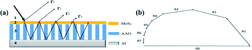 | ||
| Fig. 1 Schematic diagram of absorption principle for Al–AAO–MoS2 nanocavity structure: (a) the structure, and (b) the operation principle. | ||
In particular, the influence of the pore diameter and depth of the AAO template on the reflectance of the resonant cavity structure was studied. Fig. 2(a) and (b) display the relationships between the reflectivity, the pore depth of the AAO template and the light wavelength in the Al–AAO–MoS2 and Al–AAO structures at the relative refractive index n of 0.6 (the ratio of the actual refractive index to the refractive index of alumina). Overall, the reflectivity of the Al–AAO–MoS2 structure was smaller than that of Al–AAO, and three valleys with very weak light reflections could be observed in the Al–AAO–MoS2 structure. For example, the light reflections of the samples with the pore depths in AAO templates of 25–50 nm, 80–100 nm and 140–160 nm, respectively, were the weakest, being no more than 25% at the wavelength of 200 nm. Fig. 2(c) and (d) depict the relationship between the light reflection, the relative refractive index and the light wavelength at the AAO template thickness of 100 nm. It can be seen that when the relative refractive index is greater than 0.2 but less than 0.6, the light reflection is less than 50% in almost all the spectral ranges, achieving its minimum of 25%. When the relative refractive index exceeds 0.6, a light reflection peak will appear in the wavelength range of 200–400 nm. Therefore, in order to obtain large light absorption, we attempted to choose a medium with a relatively low refractive index so that the AAO template thickness was 40–130 nm.
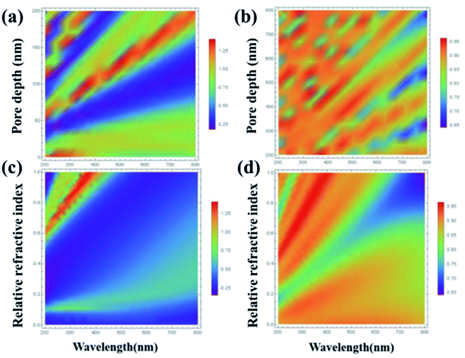 | ||
| Fig. 2 The relationship between light reflectivity and wavelength, AAO pore depth and relative refractive index of (a) and (c) Al–AAO–MoS2, and (b) and (d) Al–AAO. | ||
We also studied the effect of relative refractive index on the light absorption. Fig. 3 displays the correlation plots between the reflectivity of light, the pore depth in the AAO template, and the wavelength for the Al–AAO–MoS2 structure at the given relative refractive index. We found that the blue and purple regions with the smaller reflections gently decreased with the increase of the relative refractive index, while the green and red regions corresponding to the stronger reflections gradually increased. Moreover, as the relative refractive index increases, the period of light reflection increases with the change of pore depth in the AAO template. For example, at n = 0.6, there are three blue bands in the spectrum. In turn, their number increases to four and five at n = 0.8 and n = 1, respectively. This can be easy interpreted from the physical viewpoint: when the optical path is fixed, i.e., at 2π, the refractive index is inversely proportional to the thickness of the medium. As the refractive index increases, the thickness of the medium required to reach the corresponding optical path decreases. Therefore, the increase in the relative refractive index will result in more periodic changes.
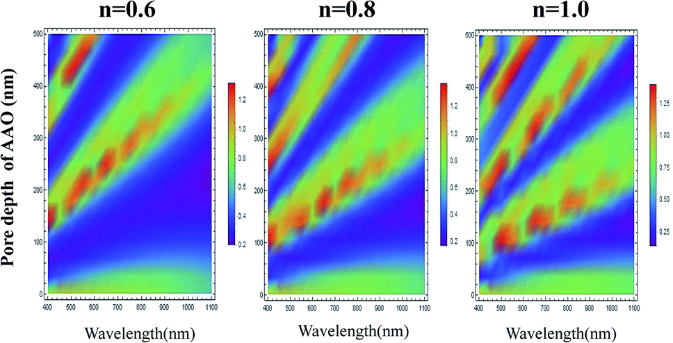 | ||
| Fig. 3 The relationship between the light reflection of the Al–AAO–MoS2 and the wavelength, the AAO pore depth under different relative refractive indexes. | ||
3.2 Experimental implementation
The main factors affecting the pore size and depth in the AAO template under the condition of fixed electrolyte include the oxidation voltage, oxidation time, and pore widening time. During the growth of AAO template, the oxidation voltage and the secondary oxidation time have a decisive influence on the size and depth of pores. Beyond that, when other parameters are fixed, the widening time exerts a direct impact on the pore size: the longer is the widening time, the larger is the pore diameter. Fig. 4(a) and (b) display the surface morphologies of the AAO templates prepared at different pore widening time and the oxidation voltages of 40 V in 0.3 mol L−1 oxalic acid. The AAO templates exhibit the regular porous array structures with cylindrical shape and uniform pore size distributions, where the channels are strictly parallel to each other. The AAO template produced at the pore widening time of 20 min has the larger pore diameter than that after 15 min of widening. As the second oxidation time increases, the pore depth of the AAO template gradually increases. Fig. 4(c) and (d) show the cross sections of AAO templates obtained at different secondary oxidation times and the oxidation voltage of 40 V. It is evident that the pore depth of the AAO template after 4 min of secondary oxidation exceeded that corresponding to 2 min of the reaction.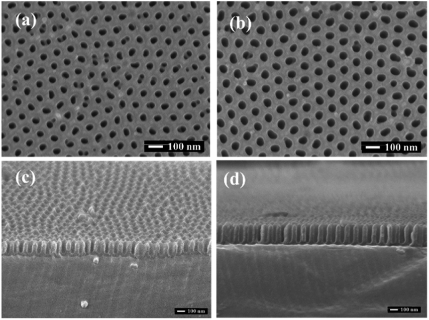 | ||
| Fig. 4 SEM images of AAO templates prepared with the secondary oxidation time of 2 min and pore widening time of (a) 15 min and (b) 20 min, and with pore widening time of 20 min and the secondary oxidation time of (c) 2 min and (d) 4 min under oxidation voltages of 40 V. | ||
Fig. 5 depicts the optical micrographs of the triangular MoS2 films grown onto the Si/SiO2 substrates and transferred to the Al–AAO template, respectively. It can be seen that the monolayer MoS2 with a microscale size is obtained by the method, and the monolayer MoS2 is still in μm-scale after transferred. In addition, the transferred sample still maintained the morphology with pronounced edges. It is obvious that the transferred MoS2 appears as the darker area, which indicates that the sample absorbs more light energy. The black dots on Fig. 5(b) should be the residual PMMA particles with small sizes, but few of them are above the sample. Therefore, their impact on the further optical characterization of the specimens will be insignificant. Meanwhile, to perform more sophisticated experiments (such as STEM or testing of field effect transistors), residual PMMA particles were removed by heating at 200 °C for 3 h in an argon atmosphere. Fig. 5(c) displays the SEM images of Al–AAO substrates transferred with MoS2, clearly showing that the porous AAO template were covered with triangular MoS2 films. Therefore, vacancy-free continuous monolayer MoS2 films could be produced by the proposed technique without the need of multilayer growth.
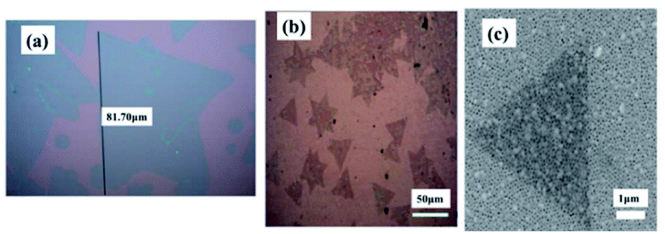 | ||
| Fig. 5 (a) The optical micrograph of MoS2 films grown on Si/SiO2 substrates, (b) the optical micrograph and (c) SEM image of the Al–AAO–MoS2 template. | ||
Raman spectroscopy is a powerful method for characterizing the interaction of matter with light. During the testing, three different points were selected for each sample to ensure the reliability of the results. The Raman spectra were recorded in a wavenumber range of 100–1000 cm−1. Since the characteristic peak of MoS2 is between 385 and 405 cm−1, the data collected on all the samples were intercepted in the wavenumber range of 370–420 cm−1, as shown in Fig. 6. Two Raman modes, referred to as E12g and A1g and corresponding to the in-plane vibrations of Mo and S atoms and the out-of-plane vibrations of S atoms, respectively, can be clearly observed.25,26 The distance between the both Raman peaks is less than 21 cm−1, which means that the MoS2 film is still a monolayer after being transferred to the substrate. Therefore, the transfer could have caused no noticeable damage to the sample. At the same time, according to Fig. 6(a), the Raman signal from the sample on the Al–AAO template is at least 15 times higher than that on the Si/SiO2 substrate. These results reveal that the resonant nanocavity structure can indeed enhance the interaction between the light and MoS2.
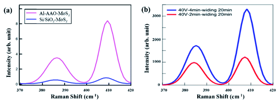 | ||
| Fig. 6 Raman results of (a) Al–AAO–MoS2 and Si/SiO2–MoS2, (b) Al–AAO–MoS2 with different second oxidation time of AAO template. | ||
Then we systematically studied the influence of the pore depth and pore diameter of the AAO template on the performance of the resonant nanocavity structure. Fig. 6(b) depicts the Raman images of Al–AAO–MoS2 with the AAO templates exposed to 2 and 4 min of the secondary oxidation, respectively, at the oxidation voltage of 40 V and the pore widening time of 20 min. The AAO template after 4 min of the reaction exhibited the larger pore depth, which, consequently, resulted in a higher Raman intensity. This is due to the same diameter of the AAO template; in that regard, the optical path will increase with increasing pore depth, approaching the thickness of ideal light absorption.
As the above calculation data, the refractive index of the dielectric layer also has a great influence on the absorption of the nanocavity structure. In the course of synthesis of the AAO template at fixed oxidation voltage and time, extending the pore widening time can increase the pore diameter of the template. Thus the AAO template with fixed pore depth and variable pore diameter was obtained. Therefore, the intermediate lossless layers of the nanocavity structures composed of the templates had the same thickness but different refractive indices. Fig. 7 shows the Raman spectra of Al/AAO/MoS2, where the AAO templates are prepared at different pore widening times and the oxidation voltages of 40 V and 60 V, respectively. It can be seen that as the widening time increases, the Raman intensity of the corresponding sample increases. This indicates that, at the same secondary oxidation time, the refractive indices of the AAO templates with identical pore depths are different owing to the variance in their pore diameters. Moreover, because of its porous structure, the AAO template can be considered as a medium composed of air and alumina, which has a refractive index between Al2O3 and air. The refractive index of the dielectric layer can be adjusted by using AAO templates with different diameters, which will change the composition ratio of air and Al2O3. At the same time, the MoS2 sample with AAO produced at an oxidation voltage of 60 V exhibits a much higher Raman scattering intensity than that of the MoS2 film at the oxidation voltage of 40 V. From the perspective of factors affecting the growth of AAO templates, the pore diameter of the AAO template prepared at the larger oxidation voltage is also larger, which results in a lower relative refractive index. After 2 min of the oxidation, the AAO template obtained at 60 V is found to exert a positive influence on the light–matter interaction in the monolayer MoS2 film.
 | ||
| Fig. 7 Raman spectroscopy of Al–AAO–MoS2 with different AAO template. | ||
Fig. 8 shows the UV-Vis spectra of the MoS2 film deposited on the Si/SiO2 substrate and the Al–AAO template, respectively. The samples exhibit the multiple peaks attributed to the periodic resonance absorption. The spectral positions of the reflectivity valleys, corresponding to the absorption maxima, were analysed accordingly. Since the light absorption of the MoS2 film is between 400 and 500 nm, we mainly study this wavelength range of Al–AAO–MoS2, where the AAO template exposed to 2 min of the secondary oxidation at the oxidation voltage of 60 V and the pore widening time of 5 min. According to the results, transferring MoS2 to the AAO template enabled one to enhance the light absorption by 50% as compared to the film directly deposited onto the Si/SiO2 substrate. Thus, the nano-cavity structure can significantly improve the light absorption properties of the entire material.
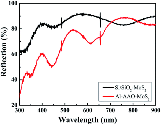 | ||
| Fig. 8 Reflection spectra of Si/SiO2–MoS2 and Al–AAO–MoS2 structures. | ||
4. Conclusions
We designed a resonant Al/AAO/MoS2 trilayer nanocavity structure. And successfully transferred a monolayer MoS2 film with atomic thickness at maintaining its structure and physical properties to AAO template. The AAO template with adjustable pore diameter and depth was introduced into the nanocavity structure to control the thickness and refractive index of the dielectric layer therein. This work effectively enhances the light–matter interaction of a single layer of MoS2.Therefore, the findings of present work open up new prospects for the improvement of the optical absorption of other two-dimensional or thin-film semiconductor materials.Conflicts of interest
There are no conflicts to declare.Acknowledgements
This research was funded by National Natural Science Foundation of China, grant number 52002266, Postdoctoral Research Foundation of China, grant number 2020M673384, Shanxi Province Science Foundation for Youths, grant number 201801D221142, and Scientific and Technological Innovation Programs of Higher Education Institutions in Shanxi, grant number 2019L0786.References
- K. S. Novoselov, A. K. Geim, S. V. Morozov, D. Jiang, Y. Zhang, S. V. Dubonos, I. V. Grigorieva and A. A. Firsov, Science, 2004, 306, 666–669 CrossRef CAS PubMed.
- X. Zhou, H. Sun and X. Bai, Frontiers in Bioengineering and Biotechnology, 2020, 8, 236 CrossRef PubMed.
- S. Y. Zhou, G.-H. Gweon, A. V. Fedorov, P. N. First, W. A. de Heer, D.-H. Lee, F. Guinea, A. H. Castro Neto and A. Lanzara, Nat. Mater., 2007, 6, 770–775 CrossRef CAS PubMed.
- H. Zeng, J. Dai, W. Yao, D. Xiao and X. Cui, Nat. Nanotechnol., 2012, 7, 490–493 CrossRef CAS PubMed.
- V. G. Kravets, F. Wu, G. H. Auton, T. Yu, S. Imaizumi and A. N. Grigorenko, npj 2D Mater. Appl., 2019, 3, 36 CrossRef.
- K. F. Mak, C. Lee, J. Hone, J. Shan and T. F. Heinz, Phys. Rev. Lett., 2010, 105, 136805 CrossRef PubMed.
- F. Aryeetey, S. Pourianejad, O. Ayanbajo, K. Nowlin, T. Ignatova and S. Aravamudhan, RSC Adv., 2021, 11, 20893–20898 RSC.
- C. Zhou, X. Wang, S. Raju, Z. Lin, D. Villaroman, B. Huang, H. L.-W. Chan, M. Chan and Y. Chai, Nanoscale, 2015, 7, 8695–8700 RSC.
- I. Shlyakhov, K. Iakoubovskii, S. Banerjee, A. Gaur, D. Lin, I. Asselberghs, I. Radu, J. Chai, M. Yang, S. J. Wang, M. Houssa, A. Stesmans and V. Afanas'ev, J. Appl. Phys., 2021, 129, 155302 CrossRef CAS.
- C. Janisch, H. Song, C. Zhou, Z. Lin, A. L. Elías, D. Ji, M. Terrones, Q. Gan and Z. Liu, 2D materials, 2016, 3, 025017 CrossRef.
- V. G. Kravets, F. Wu, G. H. Auton, T. Yu, S. Imaizumi and A. N. Grigorenko, 2D Materials and Applications, 2019, 36, 1–10 Search PubMed.
- X. Gan, Y. Gao, K. F. Mak, X. Yao, R.-J. Shiue, A. van der Zande, M. E. Trusheim, F. Hatami, T. F. Heinz, J. Hone and D. Englund, Appl. Phys. Lett., 2013, 103, 181119 CrossRef PubMed.
- D. Bouhafs, A. Moussi, A. Chikouche and J. M. Ruiz, Sol. Energy Mater. Sol. Cells, 1998, 52, 79–93 CrossRef CAS.
- S. Y. Lien, D. S. Wuu, W. C. Yeh and J. C. Liu, Sol. Energy Mater. Sol. Cells, 2006, 90, 2710–2719 CrossRef CAS.
- F. J. Rodriguez, D. E. Aznakayeva, O. P. Marshall, V. G. Kravets and A. N. Grigorenko, Adv. Mater., 2017, 29, 1606372 CrossRef PubMed.
- M. A. Kats, R. Blanchard, S. Ramanathan and F. Capasso, Opt. Photonics News, 2014, 25, 40–47 CrossRef.
- M. A. Kats, R. Blanchard, P. Genevet and F. Capasso, Nat. Mater., 2013, 12, 20–24 CrossRef CAS PubMed.
- H. Song, L. Guo, Z. Liu, K. Liu, X. Zeng, D. Ji, N. Zhang, H. Hu, S. Jiang and Q. Gan, Adv. Mater., 2014, 26, 2737–2743 CrossRef CAS PubMed.
- C. Deng, H. Song, J. Parry, Y. Liu, S. He, X. Xu, Q. Gan and H. Zeng, Nano Energy, 2018, 50, 750–755 CrossRef CAS.
- Q. Wei, Y. Fu, G. Zhang, D. Yang, G. Meng and S. Sun, Nano Energy, 2019, 55, 234–259 CrossRef CAS.
- H. Masuda and K. Fukuda, Science, 1995, 268, 1466–1468 CrossRef CAS PubMed.
- P. Taheri, J. Wang, H. Xing, J. F. Destino, M. M. Arik, C. Zhao, K. Kang, B. Blizzard, L. Zhang, P. Zhao, S. Huang, S. Yang, F. V. Bright, J. Cerne and H. Zeng, Mater. Res. Express, 2016, 3, 075009 CrossRef.
- J. S. Lee, S. W. Kim, E. Y. Jang, B. H. Kang, S. W. Lee, G. Sai-Anand, S. H. Lee, D. H. Kwon and S. W. Kang, J. Nanomater., 2015, 2015, 1–11 Search PubMed.
- C. Hsu, R. Frisenda, R. Schmidt, A. Arora, S. M. de Vasconcellos, R. Bratschitsch, H. S. J. van der Zant and A. Castellanos-Gomez, Adv. Opt. Mater., 2019, 7(13), 1900239 CrossRef.
- K. K. Liu, W. Zhang, Y. H. Lee, Y. C. Lin, M. T. Chang, C. Y. Su, C. S. Chang, H. Li, Y. Shi and H. Zhang, Nano Lett., 2012, 12, 1538–1544 CrossRef CAS PubMed.
- H. Li, Q. Zhang, C. C. R. Yap, B. K. Tay, T. H. T. Edwin, A. Olivier and D. Baillargeat, Adv. Funct. Mater., 2012, 22, 1385–1390 CrossRef CAS.
Footnote |
| † These authors contribute equally to this work. |
| This journal is © The Royal Society of Chemistry 2021 |