
 Open Access Article
 This Open Access Article is licensed under a Creative Commons Attribution-Non Commercial 3.0 Unported Licence
Vertically stacked GaN/WX2 (X = S, Se, Te) heterostructures for photocatalysts and photoelectronic devices
Dahua Ren *ab,
Yunhai Lib and
Wenqi Xiongb
*ab,
Yunhai Lib and
Wenqi Xiongb
aSchool of Information Engineering, Hubei Minzu University, Enshi, 44500, China. E-mail: rdh_perfect@163.com
bScience of Physics and Technology, Wuhan University, Wuhan, 430072, China
First published on 5th November 2021
Abstract
Tremendous attention has been paid to vertically stacked heterostructures owing to their tunable electronic structures and outstanding optical properties. In this work, we explore the structural, electronic and optical properties of vertically stacked GaN/WX2 (X = S, Se, Te) heterostructures using density functional theory. We find that these stacking heterostructures are all semiconductors with direct band gaps of 1.473 eV (GaN/WTe2), 2.102 eV (GaN/WSe2) and 1.993 eV (GaN/WS2). Interestingly, the GaN/WS2 heterostructure exhibits a type-II band alignment, while the other two stackings of GaN/WSe2 and GaN/WTe2 heterostructures have type-I band alignment. The optical absorption of GaN/WX2 heterostructures is very efficient in the visible light spectrum. Our results suggest that GaN/WX2 heterostructures are promising candidates for photocatalytic water splitting and photoelectronic devices in visible light.
Introduction
Van der Waals (vdW) heterostructures (HS) are used to design unusual electronic devices because of their peculiar physical properties and immense performances.1 Additionally, vertically stacked heterostructures have innovative applications in electronic devices, such as ultrathin photodetectors,2 solar cells,3 memory devices,4 flexible sensors and transistors5,6 etc. Specifically, two-dimensional (2D) vdW heterostructures with type-II band alignments have promising potential in photovoltaics devices and photocatalysts7–11 due to their fascinating electronic and optical properties. In type-II heterostructures, the photogenerated holes and electrons become spatially located in different layers. As a result, the recombination of carriers can be effectively prevented and the light energy utilization is significantly enhanced.12 Moreover, 2D WX2 (X = S, Se, Te) is a typical layered transition metal dichalcogenide family, which has a direct band gap from 1.0 eV to 2.4 eV.13–22 Among the transition metal dichalcogenides (TMD) materials, monolayer WS2, WSe2, and 1H WTe2 are typically semiconductors with direct band gaps of 2.38 eV,18,19 2.11 eV,20,21 1.46 eV.22Motivated by 2D graphene-like planar honeycomb structures, 2D group III–V compound semiconductors with planar hexagonal structures have been predicted to be stable.23–26 In particular, the monolayer hexagonal structure of gallium nitride (GaN) has recently received growing attractions, which has been directly experimentally synthesized via graphene encapsulation.25 Onen et al. reported that the indirect band gap of 2D GaN is 3.42 eV with HSE06 calculation,26 but the indirect bandgap hindered the practical applications in optoelectronics. In addition, heterostructures based on 2D GaN, such as GaN/blueP, GaN/MoS2, GaN/MoSe2, GaN/WS2, MoSe2/blueP, GaN/ZnO and GaN/BP heterostructures, are able to be formed to type-II band structures, which show good electronic and optical behaviors in photocatalyst and optoelectronic applications.27–32
It is also worth to note that 2D WX2, together with 2D GaN, can form vdW heterostructures for their similar structures and same lattice constants. Generally, the superior structures and excellent properties of GaN/WX2 (X = S, Se, Te) heterostructures are significantly valuable to explore, which could potentially provide a platform for applications in photocatalyst and optoelectronic devices.
Computational methods
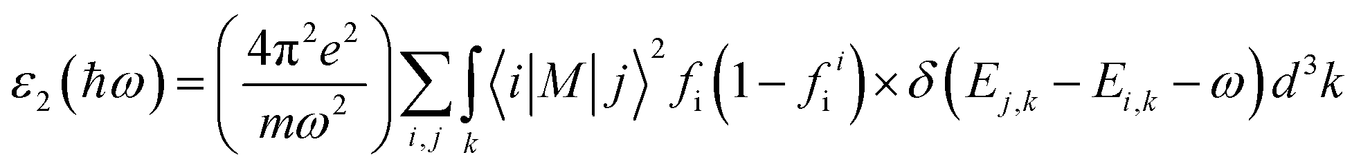
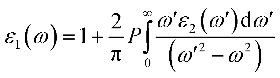
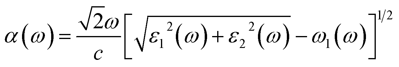
Ab initio calculations were performed within the framework of density functional theory (DFT),33,34 as implemented in the Vienna Ab Initio Simulations Package (VASP).35 Electronic exchange and correlation effects were described with the Perdew–Burke–Ernzerhof (PBE)36 functional of generalized gradient approximation (GGA)37 and HSE06 hybrid function.38 Electron–ion interaction were treated with the projector augmented wave (PAW) method,39,40 with an energy cutoff of 550 eV. And Brillouin zone sampling of K-mesh was set to 9 × 9 × 1 for relaxation. Subsequently, K-mesh points for density of states (DOS) and energy band structures were set to 13 × 13 × 1 and the energy criteria were set as 10−5 eV until the residual force was smaller than 10−3 eV Å−1. Especially, the vacuum layer thickness was set more than 25 Å to avoid spurious interactions in the neighboring images. As the long-range vdW interaction is important to hold the 2D heterostructure together, the vdW-D3 approach41 was used to describe long-range electron correlation effects.The optical properties of 2D GaN/WX2 heterostructures are described by the complex dielectric function ε(ω) = ε1(ω) + iε2(ω), where ε1(ω) and ε2(ω) are real and imaginary parts, respectively. At the same time, the imaginary part is calculated by summing up all possible transitions from the occupied to unoccupied states, which is closely related to the band structure in the absorption behaviors.42 The imaginary part is given by:
 | (1) |
 | (2) |
 | (3) |
Results and discussion
Stability and structures
Stacking patterns can modulate the electronic properties of the vdW heterostructures. Therefore, four typical stacking configurations (AA, AB, AC, AD) have been constructed. In the AA stacking, the Ga atom sits on the top of S/Se/Te atom, while the N atom is on top of W atom. In the AB stacking, the Ga atom is placed on the top of W atom, while the N atom is on the center of the hexagonal site. In the AC stacking, the N atom sits on the top of W atom, while the Ga atom is located on the center of the hexagonal site. In the AD stacking, the Ga atom sits on the top of W atom, while the N atom is on top of S/Se/Te atom. These relaxed structures are shown in Fig. 1. For GaN/WS2 heterostructure, the interface binding energies of AA, AB, AC and AD stacking patterns are −27.72 meV Å−2, −27.01 meV Å−2, −26.69 meV Å−2, and −22.58 meV Å−2 respectively. In consistence with other reports,27,28 after relaxation, AA stacking of GaN/WX2 heterostructures are the most stable due to the lowest interface binding energies. AA stacking patterns are only taken into consideration in the next calculation. The equilibrium lattice constants a(b), bond lengths, bond angles of GaN monolayer, WX2 monolayer and AA stacking GaN/WX2 heterostructures, calculated with GGA–PBE, are listed in Table 1. From Table 1, the calculated lattice constants, bond lengths/angles accord well with previous reports.13,14,16,23,24,26,28 And the relaxed crystal structures of the GaN, WS2, WSe2, and WTe2 monolayers and GaN/WX2 bilayers are hexagonal. It is clear that the hexagonal unit parameters of GaN/WS2, GaN/WSe2, GaN/WTe2 heterostructures are 3.194 Å, 3.285 Å, 3.388 Å, respectively, which agree well with previous results.28,29 The lattice mismatches are expressed as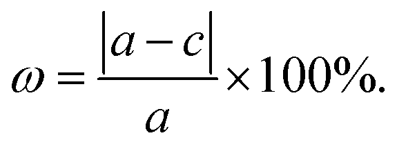 Where a and c are lattice constants of GaN/WX2 heterostructure and individual WX2 layer or GaN layer. The lattice mismatches of GaN/WS2, GaN/WSe2, GaN/WTe2 heterostructures are 1.7%, 3.0% and 3.4%, meaning that the differences are negligible.
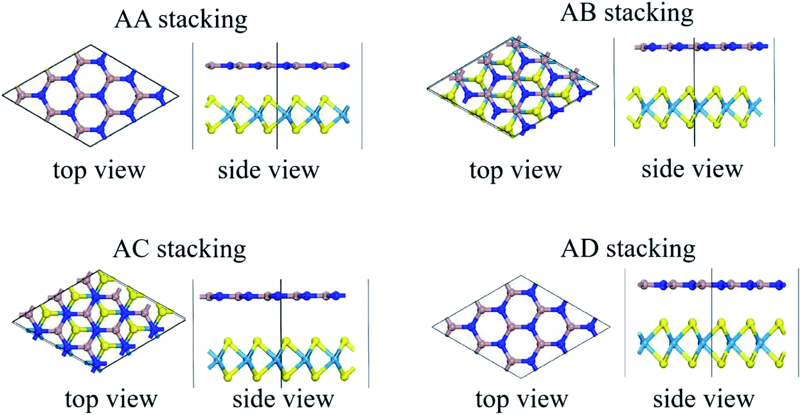 | ||
| Fig. 1 Relaxed structures of four typical stacking patterns of GaN/WX2 (X = S, Se, Te) heterostructures. Cyan, yellow, dark blue, and brown spheres indicate W, X, N and Ga atoms, respectively. | ||
| Name | a (b)/Å | lX–W/Å | lGa–N/Å | ΘXWX/° | deq/Å | ΔE/meV·Å−2 | |
|---|---|---|---|---|---|---|---|
| a Ref. 26.b Ref. 23.c Ref. 25.d Ref. 16.e Ref. 14.f Ref. 28.g Ref. 13.h Ref. 29. | |||||||
| GaN | Theo. | 3.21a, 3.25b | 1.85a | — | — | — | |
| Cal. | 3.248 | — | 1.858 | — | — | — | |
| Expt. | 3.20c | — | — | — | |||
| WS2 | Theo. | 3.18d, 3.14f | 2.42d | 81.01d | — | — | |
| Cal. | 3.185 | 2.411 | — | 81.023 | — | — | |
| Expt. | 3.155e | — | — | ||||
| WSe2 | Theo. | 3.32d, 3.31g | 2.55d | 82.43d | — | — | |
| Cal. | 3.295 | 2.517 | — | 82.749 | — | — | |
| Expt. | 3.286e | — | — | — | |||
| WTe2 | Theo. | 3.51g | — | — | — | ||
| Cal. | 3.502 | 2.736 | — | 83.334 | — | — | |
| GaN/WS2 | Theo. | 3.200f | 2.433f | 1.852h | — | 3.479f | −33.36f, −19.61h |
| Cal. | 3.194 | 2.431 | 1.845 | 81.144 | 3.081 | −27.72 | |
| GaN/WSe2 | Theo. | 3.29h | — | — | — | — | −21.87h |
| Cal. | 3.285 | 2.543 | 1.897 | 82.417 | 3.139 | −28.05 | |
| GaN/WTe2 | Cal. | 3.388 | 2.810 | 1.906 | 83.799 | 3.236 | −37.63 |
To describe the vdW interactions, the interface binding energies (ΔE) of GaN/WX2 heterostructures are calculated as:
| ΔE = (EHS − EGaN − EWX2)/S0 | (4) |
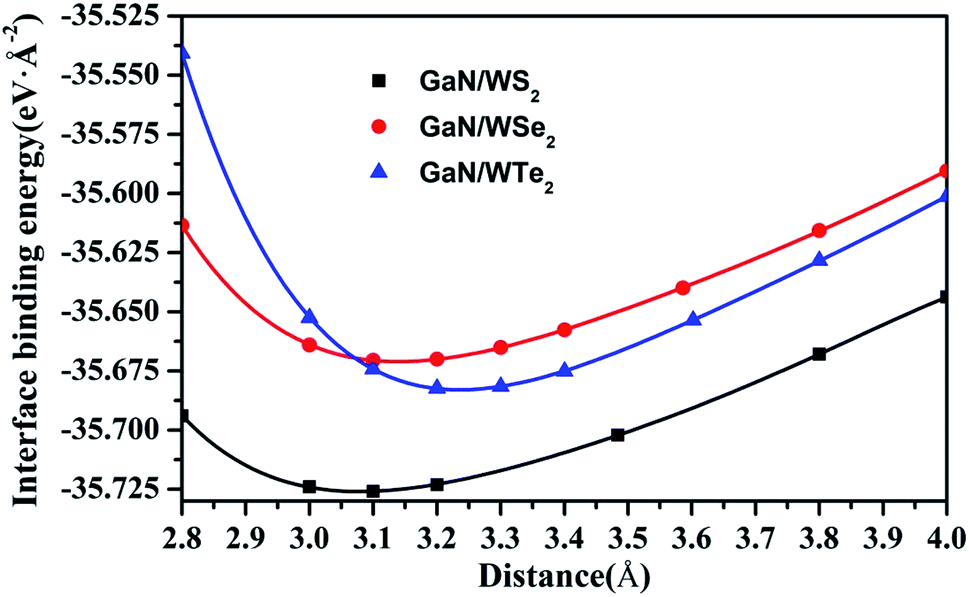 | ||
| Fig. 2 Plot of interface binding energies as function of interlayer distances for GaN/WS2, GaN/WSe2, and GaN/WTe2 heterostructures. 5th order polynomial has been employed for fitting. In order to clarify the equilibrium distances between the GaN layer and WX2 layer, the values of interface binding energies of both the GaN/WSe2 and GaN/WTe2 heterostructures are shifted downwards by 1.80 eV, 5.40 eV, respectively. | ||
Obviously, the interface binding energies of GaN/WS2, GaN/WSe2 and GaN/WTe2 heterostructures are −27.72, −28.05, and −37.63 meV Å−2, demonstrating that the interactions between two layers belong to physically vdW forces. All the interface binding energies are negative, suggesting that the GaN/WX2 heterostructures have favorable energies during the formation.
Electronic properties
In the following section, projection-resolved band structures of GaN/WX2 heterostructures are depicted in Fig. 3. All the GaN/WX2 heterostructures are direct band gap semiconductors. Both the valence band maximum (VBM) and the conduction band minimum (CBM) of the GaN/WX2 (X = S, Se, Te) heterostructures locate at the K point of Brillouin zone (BZ). The band gaps of GaN/WS2, GaN/WSe2, GaN/WTe2 heterostructures are 1.993 eV, 2.102 eV, 1.473 eV, smaller than both individual GaN (3.241 eV) layer and individual WS2 (2.357 eV), WSe2 (2.119 eV), WTe2 (1.594 eV) layer according to HSE06 calculations, which agrees well with the theoretical values of GaN (3.23 eV),23 WTe2 (1.49 eV)22 and experimental values of WS2 (2.38 eV),5 WSe2 (2.11 eV).8 Specially, GaN/WS2 heterostructure has a type II band alignment, which is beneficial to the separation of the photogenerated holes and electrons in different layers, the prevention of the recombination of carriers, and the enhancement of the light energy utilization. It is also found that the GaN/WSe2 and GaN/WTe2 heterostructures have type-I band alignment semiconductors for both the VBM and CBM of GaN/WSe2 and GaN/WTe2 heterostructures come from the W-dz2 orbitals of the WSe2 and WTe2 layer, which can be used in light emitting diodes (LED),46 indicating that the interlayer interactions between the GaN layer and the WX2 (X = Se, Te) layer reduce the band gap values. Therefore, the band gaps of the GaN/WX2 heterostructures could be significantly changed by vertically stacked heterostructures, which could provide a good opportunity to work on band engineering and electronic device designs. It is interesting that the band gap of GaN/WS2 heterostructure is larger than the minimum required energy of the photocatalytic reaction (1.23 eV), which is potential for a photocatalyst in water splitting.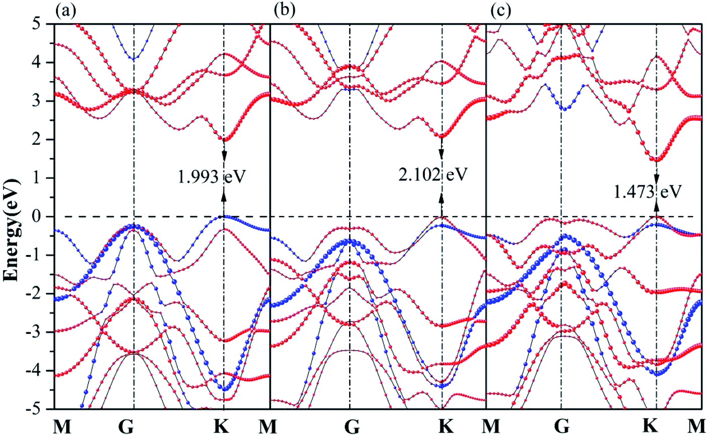 | ||
| Fig. 3 Projection-resolved band structures of (a) GaN/WS2, (b) GaN/WSe2, and (c) GaN/WTe2 heterostructures. Blue and red lines indicate contributions from GaN and WX2 layer, respectively. | ||
As reflected in the projection-resolved band structures, the band gap of WX2 monolayer is decreased by the downshift of CBM as well as the upshift of VBM at K point. The contribution of VBM of GaN/WS2 heterostructure is GaN layer and that of CBM is WS2 layer. In Fig. 4(a), the blue and red lines present the DOS of GaN and WS2 layer in GaN/WS2 heterostructure. Both the contributions of VBM and CBM of GaN/WSe2 and GaN/WTe2 heterostructures are derived from WSe2 and WTe2 layer, as shown in Fig. 4(b and c). Obviously, for GaN/WS2 heterostructure, the VBM and CBM are respectively confined in GaN and WS2 layer, which also demonstrates that GaN/WS2 heterostructure has a type-II band alignment.
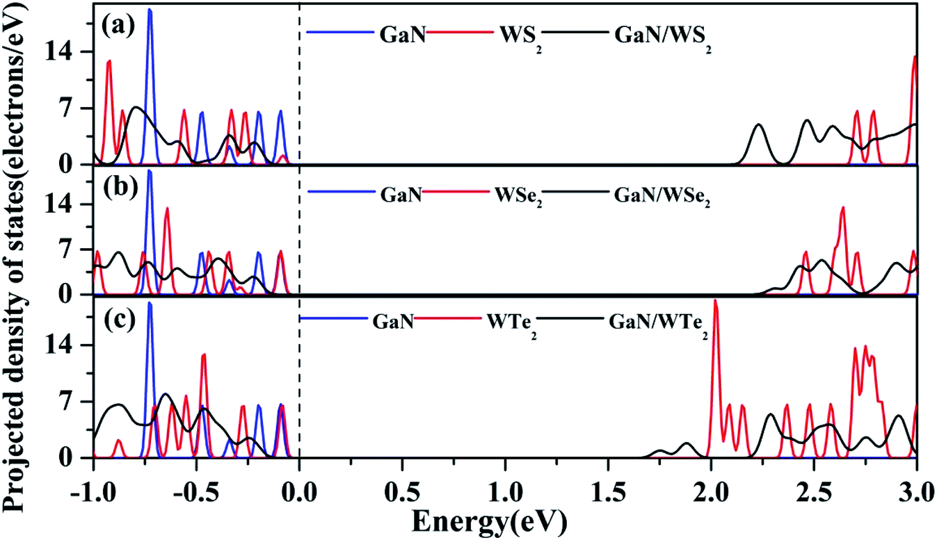 | ||
| Fig. 4 Projected density of states (PDOS) of (a) GaN/WS2, (b) GaN/WSe2, and (c) GaN/WTe2 heterostructures. Fermi level is set to zero as indicated by the black dashed line. | ||
Photocatalyst and optoelectronic performances
The absorption coefficients of GaN/WX2 heterostructures are calculated, as illustrated in Fig. 5(a). It is clear that the first peaks in absorption spectrum of GaN/WS2, GaN/WSe2, GaN/WTe2 heterostructures locate at 3.03, 2.69, 2.25 eV, which are mainly contributed by WX2 layers. The absorption spectrum of GaN/WX2 heterostructures covers the whole incident solar spectrum,47 which makes well suitable applications for optoelectronic devices in visible light.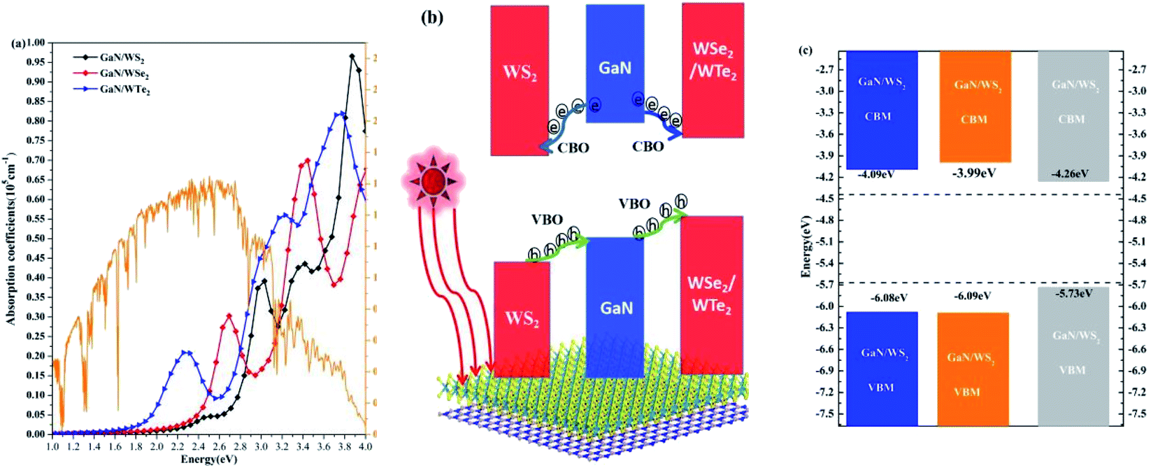 | ||
| Fig. 5 (a) Absorption spectrum of GaN/WS2, GaN/WSe2, and GaN/WTe2 heterostructures. Incident AM 1.5 G solar flux48 is plotted in orange solid line. (b) Schematic plot of the migration of photogenerated electrons and holes at the GaN/WS2 interface. (c) Band-edge alignments of GaN/WX2 heterostructures. | ||
A schematic plot of migrating carriers to depict the dynamic processes of photogenerated carriers at the GaN/WS2 interface is shown in Fig. 5(b). In the GaN/WS2 heterostructure, the photogenerated electrons start to transfer from the GaN layer the WS2 layer in the conduction band, which is motivated by the conduction band offset (CBO) (0.71 eV). Meanwhile, the photogenerated holes in the valence band move from the WS2 layer to the GaN layer, which are driven by a large valence band offset (VBO) (1.60 eV). Hence, the GaN/WS2 heterostructure, owing a type-II band alignment, could be utilized as a photocatalyst. As for the GaN/WSe2 and GaN/WTe2 heterostructures, one can see that all the photogenerated carriers of the GaN layer are likely to move to the WSe2 (WTe2) layer. The VBO and CBO between GaN and WSe2 (WTe2) layers are 1.98 eV (2.97 eV) and 0.86 eV (1.72 eV), respectively. As a result, the photogenerated carriers can be located in the WSe2 (WTe2) layers to build light-emitting diodes (LEDs).46 The band edge positions of GaN/WS2, GaN/WSe2, GaN/WTe2 heterostructures are illustrated in Fig. 5(c). The CBMs of GaN/WS2, GaN/WSe2, GaN/WTe2 heterostructures are −4.09, −3.99, −4.26 eV, respectively, whereas the VBMs of GaN/WS2, GaN/WSe2, GaN/WTe2 heterostructures are −6.08, −6.09, −5.73 eV, respectively. Those are within the oxidation potential (EO2/H2O, −5.67 eV) of water and the reduction potential (EH+/H2, −4.44 eV). Especially, the redox reaction in the GaN/WS2 heterostructure occurs in different layers: water oxidation occurs in the GaN layer, meanwhile water reduction takes place in the WS2 layer.
It is well known that the lifetime of photogenerated carriers is significantly influenced by the build-in electric field. Hence, build-in electric field induced by ground state charge transfer were investigated. Based on Bader charge analysis,48 the charge transfer from the GaN layer to the WS2 layer is 0.029e, leading to an electric field pointing to GaN from WS2. This electric field will promote the migration of electrons from the GaN layer to WS2 layer and holes from the WS2 layer to GaN layer. The build-in electric field E = P/ε0εrS0deq of 3.69 × 10⁹ V m−1 is acquired in the junction region of GaN/WS2 heterostructure. Where P = Δq·deq = 0.089e·Å is the size of dipole moment, ε0 = 8.850 × 10⁻¹² F m−1 refers to the permittivity of free space, εr = 1 represents the relative dielectric constant, S0 = 8.835 × 10⁻²⁰ m2 is the interfaces area of the WS2/GaN heterostructure, deq = 3.081 × 10⁻¹⁰ m denotes the interlayer equivalent distance.
Conclusions
In summary, the electronic and optical properties of GaN/WX2 heterostructures have been performed within density functional theory. It is found that all the hexagonal GaN/WX2 heterostructures are stable semiconductors with direct band gaps. Interestingly, among them, the GaN/WS2 heterostructure has a type-II band alignment, which is beneficial in photocatalysts for water splitting. However, both the GaN/WSe2 and GaN/WTe2 heterostructures exhibit type-I band alignment, which can be utilized in LED. In the GaN/WS2 heterostructure, the charge transport from the GaN layer to the WS2 layer is 0.029e, based on Bader charge analysis, forming a build-in electric field favorable for charge separation. The build-in electric field E = P/ε0εrS0deq of 3.69 × 10⁹ V m−1 is acquired in the junction region of GaN/WS2 heterostructure. The absorption behaviors of GaN/WX2 heterostructures are also performed, and results show that GaN/WX2 heterostructures are very efficient at absorbing the visible light to expand the application to photocatalyst and photoelectronic devices.Conflicts of interest
There are no conflicts to declare.Acknowledgements
This work is supported by the Natural Science Foundation of China with grants no. 1186040026, Incubation Project for High-Level Scientific Research Achievements of Hubei Minzu University with grants no. 4205009 and the Educational Commission of Hubei Province of China with grant no. T201914.References
- A. Geim and I. Grigorieva, Nature, 2013, 499, 419–425 CrossRef CAS PubMed.
- M. Massicotte, P. Schmidt, F. Vialla, K. G. Schädler, P. A. Reserbat, K. Watanabe, T. Taniguchi, K. J. Tielrooij and F. H. L. Koppens, Nat. Nanotechnol., 2015, 11(1), 42–46 CrossRef PubMed.
- C. H. Lee, G. H. Lee, A. M. van der Zande, W. Chen, Y. Li, M. Han, X. Cui, G. Arefe, C. Nuckolls, T. F. Heinz, J. Guo, J. Hone and P. Kim, Nat. Nanotechnol., 2014, 9(9), 676–681 CrossRef CAS PubMed.
- L. Britnell, R. V. Gorbachev, R. Jalil, B. D. Belle, F. Schedin, A. Mishchenko, T. Georgiou, M. I. Katsnelson, L. Eaves, S. V. Morozov, N. M. R. Peres, J. Leist, A. K. Geim, K. S. Novoselov and L. A. Ponomarenko, Science, 2012, 335(6071), 947–950 CrossRef CAS PubMed.
- H. Wang, H. Yuan, H. S. Sae, Y. Li and Y. Cui, Chem. Soc. Rev., 2015, 44(9), 2664–2680 RSC.
- N. Lu, H. Guo, L. Li, J. Dai, L. Wang, W. N. Mei, X. Wu and X. C. Zeng, Nanoscale, 2014, 6(5), 2879–2886 RSC.
- Z. Y. Zhu, K. Ren, H. B. Shu, Z. Cui, Z. M. Huang, J. Yu and Y. J. Xu, Catalyst, 2021, 11(8), 991 CrossRef CAS.
- Y. C. Fan, X. K. Ma, X. B. Liu, J. R. Wang, H. Q. Ai and M. W. Zhao, J. Phys. Chem. C, 2018, 122(49), 27803–27810 CrossRef CAS.
- J. B. Lou, K. Ren, Z. M. Huang, W. Y. Huo, Z. Y. Zhu and J. Yu, RSC Adv., 2021, 11(47), 29576–29584 RSC.
- K. Ren, R. X. Zheng, P. Xu, D. Cheng, W. Y. Huo, J. Yu, Z. R. Zhang and Q. Y. Sun, Nanomaterials, 2021, 11(9), 2236 CrossRef CAS PubMed.
- J. Linghu, T. Yang, Y. Luo, M. Yang, J. Zhou, L. Shen and Y. P. Feng, ACS Appl. Mater. Interfaces, 2018, 10(38), 32142–32150 CrossRef CAS PubMed.
- B. Peng, G. Yu, X. Liu, B. Liu, X. Liang, L. Bi, L. Deng, T. C. Sum and K. P. Loh, 2D Mater., 2016, 3(2), 025020 CrossRef.
- A. Kumara and P. K. Ahluwalia, Eur. Phys. J. B, 2012, 85, 186 CrossRef.
- W. S. Yun, S. W. Han, S. C. Hong, I. G. Kim and J. D. Lee, Phys. Rev. B: Condens. Matter Mater. Phys., 2012, 85(3), 033305 CrossRef.
- H. Shu, Y. Tong and J. Guo, Phys. Chem. Chem. Phys., 2017, 19(16), 10644–10650 RSC.
- C. H. Chang, Phys. Rev. B: Condens. Matter Mater. Phys., 2013, 88, 195420 CrossRef.
- B. J. Wang, X. H. Li, R. Zhao, X. L. Cai, W. Y. Yu, W. B. Li, Z. S. Liu, L. W. Zhang and S. H. Ke, J. Mater. Chem. A, 2018, 6(19), 8923–8929 RSC.
- H. M. Hill, A. F. Rigosi, K. T. Rim, G. W Flynn and T. F. Heinz, Nano Lett., 2016, 16, 4831–4837 CrossRef CAS PubMed.
- A. F. Rigosi, H. M. Hill, Y. Li, A. Chernikov and T. F. Heinz, Nano Lett., 2015, 15(8), 5033–5038 CrossRef CAS PubMed.
- S. Y. Gao, L. Yang and C. D. Spataru, Nano Lett., 2017, 17, 7809–7813 CrossRef CAS PubMed.
- S. Park, N. Mutz, T. Schultz, S. Blumstengel, A. Han, A. Aljarb, L. J. Li, E. J. W. List-Kratochvil, P. Amsalem and N. Koch, 2D Mater., 2018, 5, 025003 CrossRef.
- V. Wang, Y. Y. Liang, Y. Kawazeo and W. T. Geng, 2018, arXiv:1806.04285.
- H. L. Zhuang, A. K. Singh and R. G. Hennig, Phys. Rev. B: Condens. Matter Mater. Phys., 2013, 87(16), 165415 CrossRef.
- H. B. Shu, X. H. Niu and X. J. Ding, Appl. Surf. Sci., 2019, 479, 475–481 CrossRef CAS.
- Z. Y. Al Balushi, K. Wang, R. K. Ghosh, R. A. Vila, S. M. Eichfeld, J. D. Caldwell, X. Qin, Y. C. Lin, P. A. DeSario, G. Stone, S. Subramanian, D. F. Paul, R. M. Wallace, S. Datta, J. M. Redwing and J. A. Robinson, Nat. Mater., 2016, 15, 1166 CrossRef CAS PubMed.
- A. Onen, D. Kecik, E. Durgun and S. Ciraci, Phys. Rev. B: Condens. Matter Mater. Phys., 2016, 93, 085431 CrossRef.
- M. L. Sun, J. P. Chou, J. Yu and W. C. Tang, Phys. Chem. Chem. Phys., 2017, 19, 17324 RSC.
- H. B. Shu, Mater. Sci. Eng., B, 2020, 261, 114672 CrossRef CAS.
- Z. Cui, K. Ren, Y. M. Zhao, X. Wang, H. B. Shu, J. Yu, W. C. Tang and M. L. Sun, Appl. Surf. Sci., 2019, 492, 513–519 CrossRef CAS.
- H. B. Shu, M. L. Zhao and M. L. Sun, ACS Appl. Nano Mater., 2019, 2, 6482–6491 CrossRef CAS.
- H. B. Shu, Y. Yang and M. L. Sun, Phys. Chem. Chem. Phys., 2019, 21, 15760 RSC.
- H. B. Shu, Mater. Adv., 2020, 1, 1849 RSC.
- P. Hohenberg and W. Kohn, Phys. Rev., 1964, 136, B864 CrossRef.
- B. Y. Tong and L. J. Sham, Phys. Rev., 1966, 144(1), 1–4 CrossRef CAS.
- G. Kresse and J. Hafner, Phys. Rev. B: Condens. Matter Mater. Phys., 1993, 47, 558–561 CrossRef CAS PubMed.
- J. P. Perdew, J. P. Burke and M. Ernzerhof, Phys. Rev. Lett., 1996, 77, 3865–3868 CrossRef CAS PubMed.
- K. Burke, J. P. Perdew and M. Ernzerhof, Int. J. Quantum Chem., 1997, 61, 287–293 CrossRef CAS.
- J. Heyd, G. E. Scuseria and M. Ernzerhof, J. Chem. Phys., 2003, 118, 8207–8215 CrossRef CAS.
- G. Kresse and D. Joubert, Phys. Rev. B: Condens. Matter Mater. Phys., 1999, 59, 1758–1775 CrossRef CAS.
- P. E. Blöchl, Phys. Rev. B: Condens. Matter Mater. Phys., 1994, 50, 17953–17979 CrossRef PubMed.
- S. Grimme, J. Antony, S. Ehrlich and H. Krieg, J. Chem. Phys., 2010, 132, 154104 CrossRef PubMed.
- M. Gajdoš, K. Hummer, G. Kresse, J. Furthmüller and F. Bechstedt, Phys. Rev. B: Condens. Matter Mater. Phys., 2006, 73, 045112 CrossRef.
- S. L. Adler, Phys. Rev., 1962, 126, 413–420 CrossRef.
- H. Komsa and A. V. Krasheninnikov, Phys. Rev. B: Condens. Matter Mater. Phys., 2013, 88, 085318 CrossRef.
- X. Chen, F. Tian, C. Persson, W. Duan and N. X. Chen, Sci. Rep., 2013, 3, 3046 CrossRef PubMed.
- S. Nakamura, M. Senoh, N. Iwasa and S. I. Nagahama, Jpn. J. Appl. Phys., 1995, 34, L797 CrossRef CAS.
- The AM 1.5 G Spectrum was taken from the NREL website: https://Rredc.Nrel.Gov/Solar/Spectra/Am1.5 and integrated with the trapezoid rule.
- E. Sanville, S. D. Kenny, R. Smith and G. Henkelman, J. Comput. Chem., 2007, 28, 899–908 CrossRef CAS PubMed.
| This journal is © The Royal Society of Chemistry 2021 |