DOI:
10.1039/D1RA07112B
(Paper)
RSC Adv., 2021,
11, 34095-34100
Photoluminescence properties of cuprous phosphide prepared through phosphating copper with a native oxide layer†
Received
23rd September 2021
, Accepted 14th October 2021
First published on 21st October 2021
Abstract
Although cuprous phosphide (Cu3P) has been widely studied and applied in other fields, its photoluminescence (PL) properties are rarely investigated. Herein, we report that Cu3P can emit near-infrared light at 750 nm. We show that the annealing and the presence of cuprous oxide can enhance the PL emission. The mechanism of the PL enhancement is the improvement of crystal quality and the formation of a space charge region. Our results provide a reference for improving the PL properties of p-type semiconductors.
1. Introduction
Near-infrared light has important applications in various fields, such as communication, sensing, physics, chemistry and biology.1–9 For example, the infrared window of biological tissue is 700–900 nm, and the near-infrared light within this range can be used to detect blood oxygen signals.10,11 Cuprous phosphide (Cu3P) is widely used in catalysts, electrode materials and welding materials. However, as a p-type semiconductor material, its electrical and optical properties and applications have been neglected.12–19 Mu et al. synthesized self-doped colloidal copper phosphide (Cu3−XP) nanocrystals in solution using a “one-pot method” and found that Cu3−XP emitted fluorescence at 550–650 nm.20 The above reports indicate that Cu3−XP is a kind of fluorescent material, which has potential uses in fluorescence emission and photodetectors.21 However, the fluorescence emission wavelength they reported is in the visible light range, which is different from other researchers' results. Fu et al. reported that the band gap of Cu3P is 1.55 eV (in the range of infrared).22 Therefore, the fluorescence emission wavelength of Cu3P needs further study. In addition, the reported fluorescence emission intensity is low, so how to improve the intensity is also a scientific problem that needs to be studied.
Herein, we prepared the Cu3P through phosphating process and studied its photoluminescence properties in detail. We observed that the presence of cuprous oxide and annealing enhanced the fluorescence emission of Cu3P. We proposed that the mechanism of the PL enhancement is due to the band bending and the trapped carriers in the space charge region formed between cuprous phosphide and cuprous oxide. Our study provides a reference method for improving the fluorescence properties of Cu3P, which is useful for the optoelectronic applications.
2. Experimental
2.1. Preparation of cuprous phosphide film
Cuprous phosphide was prepared by a chemical reaction method.23 Sodium hyphosphite and copper with a native oxide layer were used as precursors. Sodium hyphosphite (0.05 mol) was loaded into a corundum crucible. The copper foil (1 cm × 1 cm) was put on the corundum crucible. Then the corundum crucible with precursors was placed into the corundum tube and pumped with argon as a protective gas for 20 min, and then the tube was sealed at one bar pressure. After that, the corundum tube was heated to 300 °C with a heating rate of 10 °C min−1 and held at 300 °C for 2 h. After that, the corundum tube was naturally cooled to room temperature to obtain Cu3P. During the cooling process, the residual gas in the tube was discharged into the hazardous gas treatment system. To study the effect of annealing on the crystallization and optical properties, cuprous phosphide was heated at 400, 500, 600, 700 and 800 °C for 2 h, respectively, under argon.
2.2. Acid treatment of cuprous phosphide
To investigate the effect of the presence of cuprous oxide (Cu2O) on the optical properties of Cu3P, the Cu3P sample containing Cu2O was treated in acid solution to remove Cu2O. The cuprous phosphide annealed at 400 °C was immersed in a dilute hydrochloric acid (0.5 mol L−1) solution for 60 min, then cleaned with de-ionized water and dried in the air.
2.3. Characterization
The crystal structure was conducted on an X-ray diffractometer (XRD, Thermo ARLXTRA). The surface morphology and elementary composition were analyzed on a field emission scanning electron microscopy (FSEM, FEI Apero S). Raman spectrum was performed on an HR Evo Nano (HORIBA) with a 532 nm laser. The diffuse reflectance ultraviolet visible spectrum (UV-vis DRS) was carried on a Shimadzu UV-3600. The photoluminescence spectrum (PL) was collected in an HR Evo Nano (HORIBA). The conductive type of cuprous phosphide was characterized by a hot-probe method. During the test, the hot probe connects to the positive terminal and the cold probe to the negative terminal. The voltage was measured using a Keysight 34461A digit multimeter. The probe was heated by a hot metal bar.
3. Results and discussion
3.1. SEM and EDX
Surface morphology and elemental mapping of Cu3P film are shown in Fig. 1. The film is composed of crystalline particles. Typical thickness of the film is ca. 2.7 μm (Fig. S1†). With the increase of heating temperature, the average particle size increased from 250 ± 20 nm for the sample annealed at 300 °C (Fig. 1a) to 500 ± 20 nm for the sample at 700 °C (Fig. 1e). This indicates that the Cu3P crystals were undergoing recrystallization during the annealing process, resulting the improved crystalline quality. Different from other samples, the one treated at 800 °C (Fig. 1f) shows more continuous and smoother surface, which is due to the formation of eutectic mixture of copper (from an excess of unreacted copper substrate) and Cu3P.24 To obtain the composition of the Cu3P sample annealed at 400 °C, we randomly tested the energy dispersive X-ray spectrum (EDX), shown in Fig. 1g–i. Copper and P elements are relatively evenly distributed in the test area, while oxygen is localized in some areas. This indicates that Cu3P contains a certain amount of copper oxides. The oxygen comes from the native oxide layer of copper precursor. The elemental ratios of Cu![[thin space (1/6-em)]](https://www.rsc.org/images/entities/char_2009.gif) :P:O in Cu3P samples grown at 300 °C and heat treated at 400, 500, 600, 700 and 800 °C are ca. 5:2:3, 4:1:5, 4:2:4, 4:3:3, 5:2:3, and 4:2:4, respectively (Table 1). The atomic ratio is not constant, nor does it show regularity with annealing temperature, which is due to the inhomogeneity of the sample and the error of the EDX.
:P:O in Cu3P samples grown at 300 °C and heat treated at 400, 500, 600, 700 and 800 °C are ca. 5:2:3, 4:1:5, 4:2:4, 4:3:3, 5:2:3, and 4:2:4, respectively (Table 1). The atomic ratio is not constant, nor does it show regularity with annealing temperature, which is due to the inhomogeneity of the sample and the error of the EDX.
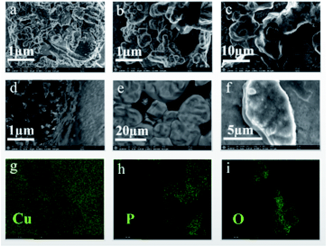 |
| | Fig. 1 SEM and EDX images of Cu3P. (a), (b), (c), (d), (e) and (f) are the SEM images of the samples grown at 300 °C and the samples heat treated at 400, 500, 600, 700 and 800 °C, respectively; (g), (h) and (i) are the distribution diagrams of Cu, P and O elements of Cu3P, respectively, corresponding to the sample heated at 400 °C. | |
Table 1 The atomic ratio (atm%) of Cu, P and O elements in Cu3P before and after annealing. The growth temperature is 300 °C, and the annealing temperature is 400 °C, 500 °C, 600 °C, 700 °C and 800 °C, respectively
| Temperature (°C) |
300 |
400 |
500 |
| Cu:P:O (atm%) |
51.1:21.8:27.1 |
41.2:11.6:47.2 |
40.8:19.2:40.0 |
| Temperature (°C) |
600 |
700 |
800 |
| Cu:P:O (atm%) |
41.0:27.7:36.3 |
49.2:23.6:27.2 |
38.2:16.5:45.3 |
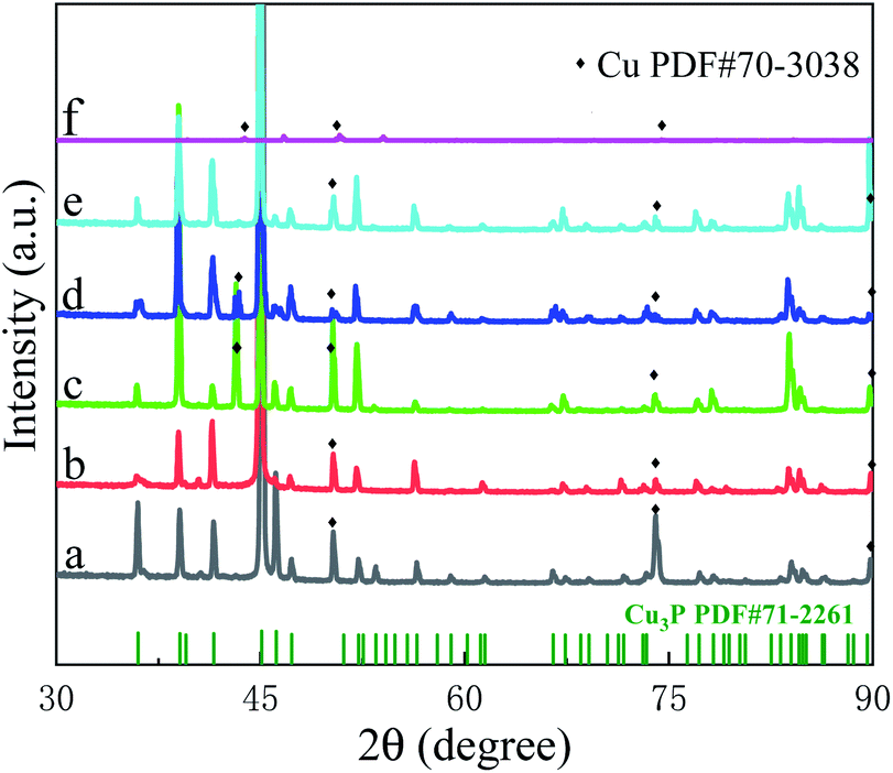
3.2. XRD
Fig. 2 is the XRD pattern of Cu3P annealed at different temperatures. The peaks without marks are corresponding to the diffraction peak of Cu3P (PDF # 71-2261).25 The peaks at 43.19°, 50.29°, 73.88° and 89.61° are derived from copper (PDF#70-3038), which comes from the excess copper precursor beneath the Cu3P. The XRD spectra are dominated by the Cu3P diffraction peaks, indicating the main component of the sample is Cu3P. As the temperature increases from 300 °C to 700 °C, the peak intensity of Cu3P changes. For example, the peak at increases 50.29° and 73.88° and decreases at 89.61°, indicating that the recrystallization process takes place and the crystallization quality improved in the process of annealing. When the temperature reaches 800 °C, the diffraction peak changes greatly: only a few diffraction peaks (47.29°, 54.09°, 84.56°) are observed according to Fig. 2f and the intensity of copper peaks increases relative to Cu3P, which are resulted from the forming of eutectic mixture. The peak position of Cu3P does not change with the annealing temperature, indicating that there is no stress inside the Cu3P crystal. Unlike the copper oxides observed by EDX data, XRD does not, which indicates that the amount of copper oxides is too low or the crystallinity is too poor for XRD.
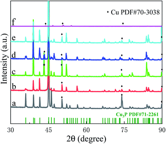 |
| | Fig. 2 XRD of Cu3P before and after annealing: (a) grown at 300 °C without annealing; annealed at (b) 400, (c) 500, (d) 600, (e) 700 and (f) 800 °C. The reference peaks of Cu3P are corresponding to PDF#71-2261. | |
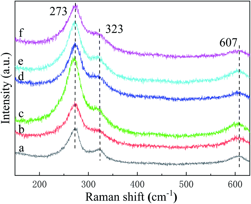
3.3. Raman
In order to further analyze the composition of the sample, we performed Raman spectroscopy. Fig. 3 shows the Raman spectra of Cu3P before and after annealing. The peaks centered at 273 cm−1 and 607 cm−1 are due to Cu3P,26 and the peak at 323 cm−1 is derived from cuprous oxide (Cu2O).27 The peak intensity of Cu3P is stronger than that of Cu2O, indicating that the main component of the sample is Cu3P combined with small amount of Cu2O. In addition, we observe that annealing has no obvious effect on the Raman peak position and peak shape, consisting with the analysis results of XRD, indicating that there is no stress in the crystal.
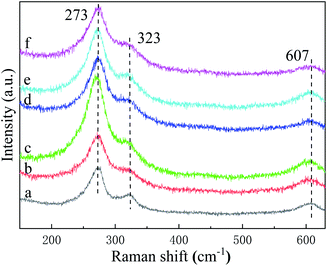 |
| | Fig. 3 Raman spectra of Cu3P before and after annealing: (a) grown at 300 °C without annealing; annealed at (b) 400, (c) 500, (d) 600, (e) 700 and (f) 800 °C, respectively. | |
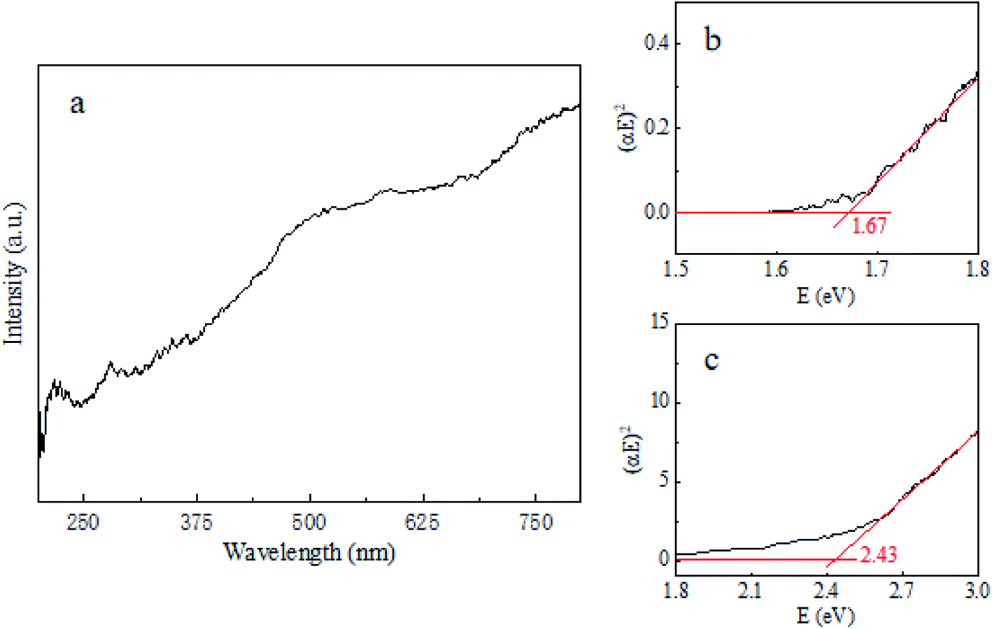
3.4. UV-vis
Fig. 4a is a typical UV-vis DRS of Cu3P. Cuprous phosphide is better at absorbing short wavelengths (less than 400 nm) than long wavelengths (from 400 nm to near-infrared light). We can find two absorption edges, located at 400–475 nm and 680–740 nm, respectively. The former is due to the absorption of Cu2O, and the latter corresponds to the absorption of Cu3P.
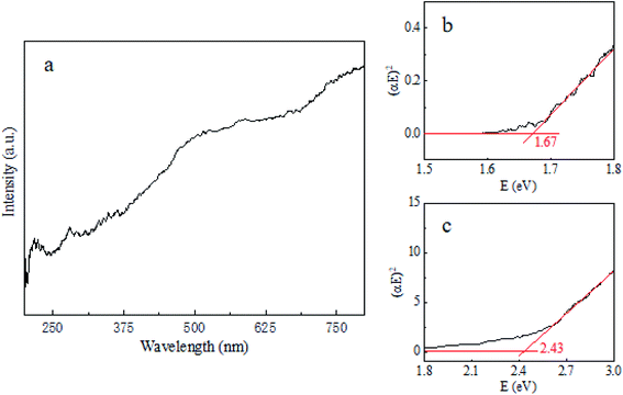 |
| | Fig. 4 Typical UV-vis diffuse reflection spectrum of Cu3P (containing cuprous oxide) (a). Tauc plot for Cu3P (b) and Cu2O (c) composites. | |
In order to obtain the optical band gap width of Cu3P, we processed UV-vis DRS data. Firstly, we converted UV-vis DRS data into absorption spectrum, then, plotted it with photon energy E as horizontal coordinate axis, and (αhv)2 as the vertical coordinate axis, as shown in Fig. 4b and c.28–30 The horizontal ordinate of the point where the extension line of the linear part of the curve intersects with the longitudinal coordinate equal to zero is the value of the band gap width. The band gaps of Cu3P and Cu2O are 1.67 eV and 2.43 eV, respectively, which are consistent with the results of other groups.22,31–34
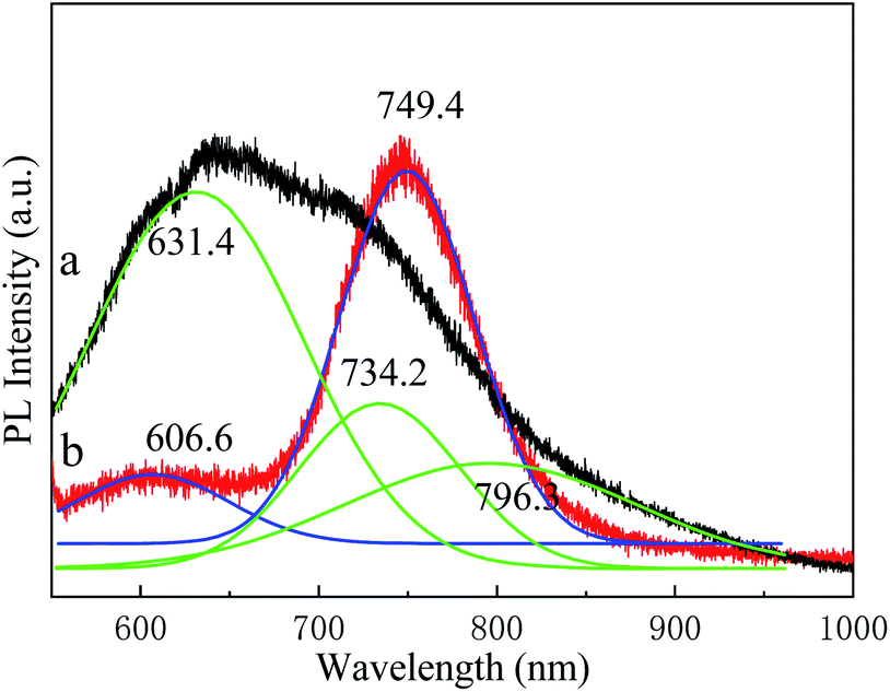
3.5. PL
Fig. 5 shows the normalized PL spectra of Cu3P before and after annealing. The spectra were fitted by a Gaussian function. Detailed data obtained by fitting are listed in Table 2. We find a broad peak ranging from 500 to 800 nm in the sample before annealing (Fig. 5a). The peak can be fitted into three subpeaks, centered at 631.4 nm, 734.2 nm and 796.3 nm, respectively. We speculate that the peak at 631.4 nm is from the band-edge fluorescence emission of Cu2O, the peak at 734.2 nm from Cu3P, and the peak at 796.3 nm from the impurity level emission of Cu3P.12,35 In addition, the PL intensity of Cu3P is weaker than that of Cu2O. After annealing, the peak of Cu2O blueshifts to 606.6 nm, and the peak of Cu3P redshifts to 749.4 nm, and the peak at 796.3 nm disappears. The shifts of the peak should be related to the improvement of the crystal quality and grain boundary. The PL emission of Cu3P is greatly enhanced, while that of Cu2O is sharply reduced. The PL intensity ratio of Cu3P to Cu2O is increased from 71% before annealing to 500% after annealing. In addition, the full width at half maximum (FWHM) of Cu3P decreases obviously after annealing. Our observation indicates that the annealing can greatly improve the fluorescence properties of Cu3P. We found that the optimal annealing temperature is 400 °C. When the annealing temperature rises to 600 °C and 700 °C, the PL intensity of Cu3P relative to Cu2O decreases, as shown in Fig. S2.† When the temperature reaches 800 °C, the PL of Cu3P is hardly even observed. We believe the annealing at higher temperature decreases crystalline quality. The Cu3P may be partially decomposed or oxidized by residual oxygen in the annealing system.
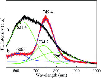 |
| | Fig. 5 Photoluminescence spectra of Cu3P grown at 300 °C (a) and annealed at 400 °C (b). The black and red curves are experimental data, while the green and blue curves are fitted curves by Gaussian function. | |
Table 2 Detailed fitting data of PL spectra of Cu3P grown at 300 °C and annealed at 400 °C, corresponding to the data in Fig. 5
| Sample |
Grown at 300 °C |
Annealed at 400 °C |
| Peak position (nm) |
631.4 |
734.2 |
796.3 |
606.6 |
749.4 |
| Assignment |
Cu2O |
Cu3P |
Defects of Cu3P |
Cu2O |
Traps in Cu3P |
| Peak intensity (peak integral area) |
124.9 |
41.0 |
47.5 |
16.3 |
77.6 |
| Full width at half maximum (FWHM) |
120.0 |
90.2 |
163.8 |
85.8 |
75.4 |
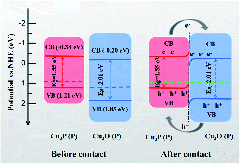
There are two reasons for the fluorescence enhancement of Cu3P by annealing: improvement of the crystal quality and existence of a space charge region.36–38 First, annealing improves the crystallization quality and reduces the impurity level, enhancing the interband emission. Secondly, annealing improves the bonding quality between Cu3P and Cu2O grain interfaces. The conductive type of Cu3P was determined by hot-probe method. Hot-probe characteristic for Cu3P is shown in Fig. S3.† The data show measured voltages are depended on the heating time. Cu3P is of p-type as negative values of measured voltages are observed under hot status.39 Both Cu3P and Cu2O are p-type semiconductors. The band gap width of Cu2O is larger than that of Cu3P. The conduction band energy level of Cu2O is slightly higher than that of Cu3P, and the valence band energy level of Cu2O is lower than that of the Cu3P, shown in Fig. 6a.22 Therefore, the hole transfer from Cu2O to Cu3P occurs and forms a space charge region at the interface when the two materials come into contact, shown in Fig. 6b. The space charge region leads to energy band bending upwards at the side of Cu3P and down at the side of Cu2O. The band energy levels stagger at the junction of the two materials to form carrier traps. The trap accumulates the photogenerated electrons and holes in the space charge region at the side of Cu3P, which enhance the near-infrared light emission of Cu3P.
 |
| | Fig. 6 Schematic diagram of photogenerated carrier transfer mechanism between Cu3P and Cu2O. See references for the energy level data.22,40 CB, VB, P, e−, h+ represent conduction band, valence band, p-type, electron and hole, respectively. | |
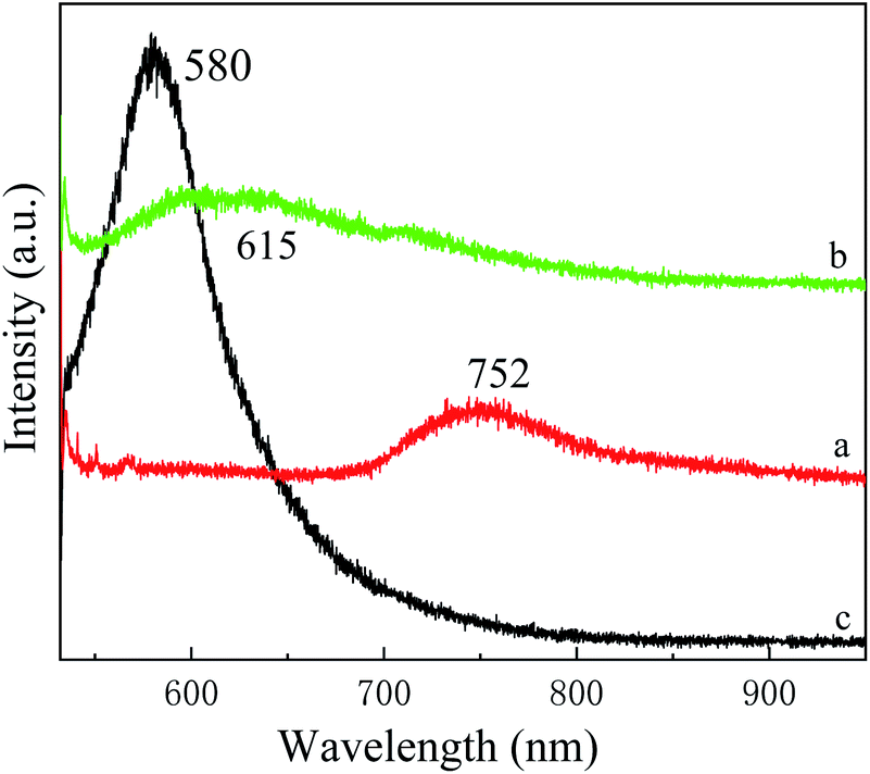
In order to verify the space charge region mechanism, we use hydrochloric acid to remove Cu2O partially to destroy the space charge region. If the space charge region were destroyed, the transfer channel of the photogenerated carrier is cut off, then the PL intensity of Cu3P should be decreased. The experimental results are shown in Fig. 7. We find the PL intensity of Cu3P decreases, and that of Cu2O increases. The results agree with our hypothesis, so our proposed mechanism is correct.
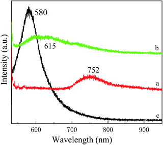 |
| | Fig. 7 Fluorescence spectra of Cu3P before (a) and after (b) hydrochloric acid treatment. Curve (c) is the fluorescence spectrum of Cu2O. The Cu3P sample was grown at 300 °C and annealed at 400 °C. | |
4. Conclusion
In this paper, the fluorescence properties of Cu3P were studied. Cuprous phosphide emitted near-infrared emission under the excitation of short wavelength light. The PL of Cu3P was affected by annealing and the presence of Cu2O. Annealing improved the crystal quality and the fluorescence property. Cuprous oxide enhanced the PL emission through the formation of space charge region. Our results show that the method of forming hole traps in p-type semiconductor can help us to obtain efficient fluorescence emission materials through energy band engineering.
Author contributions
Yanfei Lv, Li Fu, Fei Chen, Qi Zhang conceived and designed the experiments; Xue Peng and Weitao Su performed the experiments; Xue Peng prepared the manuscript; Jingzhou Li and Shichao Zhao performed the data analyses and wrote the paper.
Conflicts of interest
There are no conflicts to declare.
References
- M. T. Hasan, B. H. Lee, C. W. Lin, A. McDonald-Boyer, R. Gonzalez-Rodriguez, S. Vasireddy, U. Tsedev, J. Coffer, A. M. Belcher and A. V. Naumov, 2d Mater, 2021, 8, 035013 CrossRef.
- S. C. Park, W. S. Yang, J. Y. Ahn, J. B. Park, J. H. Lee, Y. Jung, H. R. Kim, J. Y. Kim, J. M. Lim and B. H. Hong, 2d Mater, 2021, 8, 035012 CrossRef.
- T. Horimoto, N. Kannari and K. Sato, Appl. Surf. Sci., 2021, 558, 149841 CrossRef CAS.
- L. Liu, R. Z. Li, L. Z. Zhang, P. Zhang, G. D. Zhang, S. Q. Xia and X. T. Tao, J. Alloys Compd., 2021, 874, 159943 CrossRef CAS.
- J. Qian, Y. L. Luan, M. S. Kim, K. M. Ho, Y. Shi, C. Z. Wang, Y. Li and Z. Fei, Phys. Rev. B, 2021, 103, L201407 CrossRef CAS.
- Z. C. Guo, X. R. Liu, H. Y. Yu, F. J. Hou, S. M. Gao, L. L. Zhong, H. Xu, Y. Yu, J. L. Meng and R. R. Wang, Spectrochim. Acta, Part A, 2021, 257, 119774 CrossRef CAS PubMed.
- W. Y. Ma, S. L. Yu and T. G. Zhao, Opt. Commun., 2021, 493, 127037 CrossRef CAS.
- J. W. John, V. Dhyani, S. Singh, A. Jakhar, A. Sarkar, S. Das and S. K. Ray, Nanotechnology, 2021, 32, 315205 CrossRef CAS PubMed.
- T. T. P. Hoang, V. D. Pham and T. Son, J. Nanosci. Nanotechnol., 2021, 21, 5535–5541 CrossRef CAS PubMed.
- S. A. Manea, M. L. Vlad, D. Rebleanu, A. G. Lazar, I. M. Fenyo, M. Calin, M. Simionescu and A. Manea, Oxid. Med. Cell. Longevity, 2021, 2021, 6685612 CrossRef PubMed.
- W. X. Liu, L. D. Xing, L. Y. Yao, Z. H. Zou and Y. Zhang, Zhongguo Yi Liao Qi Xie Za Zhi, 2021, 45, 280–283 Search PubMed.
- S. X. Hua, D. Qu, L. An, W. S. Jiang, Y. J. Wen, X. Y. Wang and Z. C. Sun, Appl. Catal., B, 2019, 240, 253–261 CrossRef CAS.
- P. He, J. C. Feng and H. Zhou, J. Mater. Sci. Technol., 2005, 21, 493–498 CAS.
- X. P. Xu, Q. J. Ma and C. Z. Xia, High Temp. Mater. Processes, 2019, 38, 651–661 CrossRef CAS.
- N. A. M. Zahri, F. Yusof, T. Ariga, A. S. M. A. Haseeb, M. A. Mansoor and N. L. Sukiman, Mater. Sci. Technol., 2019, 35, 2004–2012 CrossRef.
- A. Wolff, T. Doert, J. Hunger, M. Kaiser, J. Pallmann, R. Reinhold, S. Yogendra, L. Giebeler, J. Sichelschmidt, W. Schnelle, R. Whiteside, H. Q. N. Gunaratne, P. Nockemann, J. J. Weigand, E. Brunner and M. Ruck, Chem. Mater., 2018, 30, 7111–7123 CrossRef CAS.
- X. D. Zhang, J. Yan and L. Y. S. Lee, Appl. Catal., B, 2021, 283, 119624 CrossRef CAS.
- B. A. Tappan, K. Y. Chen, H. P. Lu, S. M. Sharada and R. L. Brutchey, ACS Appl. Mater. Interfaces, 2020, 12, 16394–16401 CrossRef CAS PubMed.
- L. De Trizio, R. Gaspari, G. Bertoni, I. Kriegel, L. Moretti, F. Scotognella, L. Maserati, Y. Zhang, G. C. Messina, M. Prato, S. Marras, A. Cavalli and L. Manna, Chem. Mater., 2015, 27, 1120–1128 CrossRef CAS PubMed.
- H. R. Mu, Z. K. Liu, X. Z. Bao, Z. C. Wan, G. Y. Liu, X. P. Li, H. Y. Shao, G. C. Xing, B. Shabbir, L. Li, T. Sun, S. J. Li, W. L. Ma and Q. L. Bao, Front. Optoelectron., 2020, 13, 139–148 CrossRef.
- T. Sun, Y. J. Wang, W. Z. Yu, Y. S. Wang, Z. G. Dai, Z. K. Liu, B. N. Shivananju, Y. P. Zhang, K. Fu, B. Shabbir, W. L. Ma, S. J. Li and Q. L. Bao, Small, 2017, 13(42), 1701881 CrossRef PubMed.
- Z. Y. Fu, X. Y. Ma, B. Xia, X. Y. Hu, J. Fan and E. Z. Liu, Int. J. Hydrogen Energy, 2021, 46, 19373–19384 CrossRef CAS.
- Y. Zuo, J. Shen, Y. D. Hu and R. H. Gao, J. Mater. Process. Technol., 2018, 253, 27–33 CrossRef CAS.
- T. Noda, K. Oikawa, S. Itoh, M. Hino and T. Nagasaka, Calphad, 2009, 33, 557–560 CrossRef CAS.
- J. Lin, C. H. Zeng, X. M. Lin, C. Xu and C. Y. Su, Adv. Sci., 2020, 7(14), 2000736 CrossRef CAS PubMed.
- S. L. Liu, X. D. He, J. P. Zhu, L. Q. Xu and J. B. Tong, Sci. Rep., 2016, 6, 35189 CrossRef CAS PubMed.
- B. Houng, J. K. Wu, P. C. Yeh, W. L. Yeh and C. K. Sun, J. Electroceram., 2021, 45(3), 129–134 CrossRef.
- E. A. Davis and N. F. Mott, Philosophical Magazine, 1970, 22, 0903–0922 CrossRef CAS.
- J. Tauc, R. Grigorovici and A. Vancu, Phys. Status Solidi B, 1966, 15, 627–637 CrossRef CAS.
- F. P. Yan, F. G. Yang, H. Zhang and P. H. Luo, Mater. Res. Express, 2021, 8(4), 045508 CrossRef CAS.
- R. Gaspari, F. Labat, L. Manna, C. Adamo and A. Cavalli, Theor. Chem. Acc., 2016, 135(3), 73 Search PubMed.
- T. Begildayeva, S. J. Lee, Y. Yu, J. Park, T. H. Kim, J. Theerthagiri, A. Ahn, H. J. Jung and M. Y. Choi, J. Hazard. Mater., 2021, 409, 124412 CrossRef CAS PubMed.
- A. A. Dubale, C. J. Pan, A. G. Tamirat, H. M. Chen, W. N. Su, C. H. Chen, J. Rick, D. W. Ayele, B. A. Aragaw, J. F. Lee, Y. W. Yang and B. J. Hwang, J. Mater. Chem. A, 2015, 3, 12482–12499 RSC.
- M. A. Hossain, R. Al-Gaashani, H. Hamoudi, M. J. Al Marri, I. A. Hussein, A. Belaidi, B. A. Merzougui, F.
H. Alharbi and N. Tabet, Mater. Sci. Semicond. Process., 2017, 63, 203–211 CrossRef CAS.
- T. Wu, H. Zheng, Y. C. Kou, X. Y. Su, N. R. Kadasala, M. Gao, L. Chen, D. L. Han, Y. Liu and J. H. Yang, Microsyst. Nanoeng., 2021, 7(1), 23 CrossRef CAS PubMed.
- L. Y. Zhang, F. Q. Wang, S. Wang, H. W. Huang, X. M. Meng, Y. R. Ouyang, W. Y. Yuan, C. X. Guo and C. M. Li, Adv. Funct. Mater., 2020, 30(43), 2003933 CrossRef CAS.
- F. Q. Wang, S. Wang, D. B. Wu, H. W. Huang, W. Y. Yuan and L. Y. Zhang, Appl. Surf. Sci., 2021, 537, 147860 CrossRef CAS.
- Y. Y. Gong, X. H. Liu, Y. Y. Gong, D. B. Wu, B. H. Xu, L. Bi, L. Y. Zhang and X. S. Zhao, J. Colloid Interface Sci., 2018, 530, 189–195 CrossRef CAS PubMed.
- G. Golan, A. Axelevitch, B. Gorenstein and V. Manevych, Microelectron. J., 2006, 37, 910–915 CrossRef CAS.
- J. Singh, S. Juneja, R. K. Soni and J. Bhattacharya, J. Colloid Interface Sci., 2021, 590, 60–71 CrossRef CAS PubMed.
Footnote |
| † Electronic supplementary information (ESI) available. See DOI: 10.1039/d1ra07112b |
|
| This journal is © The Royal Society of Chemistry 2021 |
Click here to see how this site uses Cookies. View our privacy policy here. 
 Open Access Article
 This Open Access Article is licensed under a Creative Commons Attribution-Non Commercial 3.0 Unported Licence
 a,
Weitao Sua,
Jingzhou Li*b,
Qi Zhanga and
Shichao Zhao
a,
Weitao Sua,
Jingzhou Li*b,
Qi Zhanga and
Shichao Zhao