
 Open Access Article
 This Open Access Article is licensed under a
 Creative Commons Attribution 3.0 Unported Licence
Adjusting the electronic properties and contact types of graphene/F-diamane-like C4F2 van der Waals heterostructure: a first principles study†
Thi-Nga Doab,
Son-Tung Nguyenc and
Cuong Q. Nguyen *de
*de
aLaboratory of Magnetism and Magnetic Materials, Advanced Institute of Materials Science, Ton Duc Thang University, Ho Chi Minh City, Vietnam. E-mail: dothinga@tdtu.edu.vn
bFaculty of Applied Sciences, Ton Duc Thang University, Ho Chi Minh City, Vietnam
cFaculty of Electrical Engineering Technology, Hanoi University of Industry, Hanoi 100000, Vietnam
dInstitute of Research and Development, Duy Tan University, Da Nang 550000, Vietnam. E-mail: nguyenquangcuong3@duytan.edu.vn
eFaculty of Natural Sciences, Duy Tan University, Da Nang 550000, Vietnam
First published on 25th November 2021
Abstract
Motivated by the successful exfoliation of two-dimensional F-diamane-like C4F2 monolayer and the superior properties of graphene-based vdW heterostructures, in this work, we perform a first principles study to investigate the atomic structure, electronic properties and contact types of the graphene/F-diamane-like C4F2 heterostructure. The graphene/C4F2 vdW heterostructure is structurally stable at room temperature. In the ground state, the graphene/C4F2 heterostructure forms n-type Schottky contact with a Schottky barrier height of 0.46/1.03 eV given by PBE/HSE06. The formation of the graphene/C4F2 heterostructure tends to decrease in the band gap of the semiconducting C4F2 layer, suggesting that such a heterostructure may have strong optical absorption. Furthermore, the electronic properties and contact types of the graphene/C4F2 heterostructure can be adjusted by applying an external electric field, which leads to the change in the Schottky barrier height and the transformation from Schottky to ohmic contact. Our findings reveal the potential of the graphene/C4F2 heterostructure as a tunable hybrid material with strong potential in electronic applications.
1 Introduction
The development of science and technology has opened the door for wide ranging materials science and engineering, especially the science of novel two-dimensional (2D) materials. Through the application of modern science and technology, such as exfoliation1–3 and chemical vapor deposition (CVD),4–6 many novel 2D materials have been successfully fabricated and investigated. Graphene, a single-atom-thick 2D material was successfully discovered by mechanical exfoliation of graphite in 2004.7 After such a discovery, a lot of novel 2D materials with unusual physical and chemical properties and wide range of potential applications, were discovered and studied, including transition metal dichalcogenides,8,9 phosphorene,10,11 MXenes12,13 and Janus-like 2D materials.14,15 Owing to their outstanding physical and chemical properties, 2D materials are promising candidates for electronics, optoelectronics and photocatalytics.16–18 However, the aforementioned 2D materials have some disadvantages that hinder their application in many advanced technologies. For instance, the lack of a band gap in graphene limits its application in high-performance nanodevices like electronics and photoelectronics.19 A small carrier mobility in 2D TMDs like MoS2 (200 cm2 V s−1 (ref. 20)) has limited its practical application. Therefore, along with finding effective strategies to modulate the properties of 2D materials, searching for novel 2D materials with the desired properties for practical applications is still challenging.Currently, there have been many effective strategies for modulating the properties of 2D materials, such as doping,21–24 functionalization25–27 and constructing 2D van der Waals heterostructures (vdWH).28–31 For instance, Pierucci et al.21 demonstrated that the structural and electronic properties of the MoS2 monolayer can be modulated by chemical doping of hydrogen atoms, which results in the transition from an n-type to p-type semiconductor. Furthermore, Muniz et al. predicted that the band gap of twisted bilayer graphene can be tuned by the substitution of chemisorbed H by F atoms,32 by the formation of diamond superlattices33 and by the formation of fullerene superlattices.34 Sun et al.35 predicted that the ability to absorb the sunlight of 2D blue phosphorene is enhanced upon defects. Very recently, F-diamane-like C4F2 2D materials, a new type of carbon allotrope have been successfully synthesized by a CVD method36 and liquid-phase exfoliation.37 The F-diamane-like C4F2 monolayer has been predicted to be stable under an ambient atmosphere.36 The F-diamane-like C4F2 possesses a semiconducting characteristic and exhibits superior carrier mobility as well as high mechanical strength and thermal conductivity.38 Furthermore, the electronic and transport properties of the F-diamane-like C4F2 monolayer are very sensitive to strain engineering38,39 and chemical functionalization.40 These aforementioned properties of the F-diamane-like C4F2 material make it a promising candidate for high-performance electronic and optoelectronic applications.
As we discussed above, the construction of vdW heterostructures is known to be one of the most effective tools to adjust the electronic properties of 2D materials. In particular, 2D-based vdW heterostructures can be fabricated in experiments by transfer methods41 or by exfoliation.42 A plethora of vdW heterostructures composed of two or more 2D materials have been fabricated experimentally and predicted theoretically, such as TMDs-based vdW heterostructures,43–46 phosphorene-based vdW heterostructures47–49 and graphene-based vdW heterostructures.50–56 Among these, graphene-based vdW heterostructures have received considerable interest owing to the existence of new properties different to the constituent materials. For instance, Aziza et al.57 showed that the Dirac cone of graphene is shifted by 100 meV toward lower binding energy upon contact between graphene and GaSe. Nguyen et al.56 predicted that the contact between graphene and a BiI3 monolayer gives rise to the formation of an n-type Schottky contact. To date, the interfacial characteristics and the electronic properties of the contact between graphene and an F-diamane-like C4F2 monolayer, have not yet been investigated.
Motivated by the successful exfoliation of 2D F-diamane-like C4F2 monolayers and the superior properties of graphene-based vdW heterostructures, in this work, we perform a first principles study to investigate the atomic structure, electronic properties and contact types of the graphene/F-diamane-like C4F2 (graphene/C4F2) vdW heterostructure. The graphene/C4F2 vdW heterostructure is structurally and thermodynamically stable at room temperature. The formation of graphene/C4F2 vdW heterostructure gives rise to the Schottky contact, which can be adjusted by an external electric field. Our findings reveal the potential of graphene/C4F2 heterostructure as a tunable hybrid material with strong potential in electronic applications.
2 Computational details
In this work, our results for the geometric optimization, electronic properties and the band alignment of the graphene/C4F2 vdWH are calculated using first-principles calculations. All calculations are carried out in the Vienna ab initio simulation (VASP)58 and Quantum Espresso![[thin space (1/6-em)]](https://www.rsc.org/images/entities/char_2009.gif) 59,60 simulation packages. The generalized gradient approximation (GGA)61 by Perdew–Burke–Ernzerhof (PBE) is employed to describe the electronic exchange and correlation. The projector augmented wave (PAW) approach62 is chosen to treat the core and valence electrons. According to the weak vdW interactions between layered 2D materials, the DFT-D3 method of Grimme63 is adopted to better describe these interactions. The underestimation of the traditional PBE method on the band gap of 2D materials leads us to use the Heyd–Scuseria–Ernzerhof (HSE06) hybrid functional to obtain a more accurate value for the band gap. The cut-off energy for the plane-wave expansion is set to be 510 eV with a 12 × 12 × 1 k-point mesh. To avoid interactions between periodical slabs, we set a large vacuum thickness of 30 Å along the z direction. The convergence of energy and force are set to be 10−6 eV and 10−3 eV Å−1, respectively.
59,60 simulation packages. The generalized gradient approximation (GGA)61 by Perdew–Burke–Ernzerhof (PBE) is employed to describe the electronic exchange and correlation. The projector augmented wave (PAW) approach62 is chosen to treat the core and valence electrons. According to the weak vdW interactions between layered 2D materials, the DFT-D3 method of Grimme63 is adopted to better describe these interactions. The underestimation of the traditional PBE method on the band gap of 2D materials leads us to use the Heyd–Scuseria–Ernzerhof (HSE06) hybrid functional to obtain a more accurate value for the band gap. The cut-off energy for the plane-wave expansion is set to be 510 eV with a 12 × 12 × 1 k-point mesh. To avoid interactions between periodical slabs, we set a large vacuum thickness of 30 Å along the z direction. The convergence of energy and force are set to be 10−6 eV and 10−3 eV Å−1, respectively.
3 Results and discussion
We first explore the atomic structure and electronic properties of the F-diamane-like C4F2 monolayer. After geometric optimization, the atomic structure of single-layered F-diamane-like C4F2 is as depicted in Fig. 1(a). The F-diamane-like C4F2 monolayer has a layered buckling structure. The lattice constant of F-diamane-like C4F2 monolayer is calculated to be 2.54 Å, which shows good agreement with the experimental value37 and theoretical reports.39 The electronic band structures as well as the weighted band structure of the F-diamane-like C4F2 monolayer are depicted in Fig. 1(b–d). The F-diamane-like C4F2 monolayer exhibits a semiconducting characteristic with a direct band gap. Both the valence band maximum (VBM) and conduction band minimum (CBM) of the F-diamane-like C4F2 monolayer are located at the Γ point for both PBE and HSE06 method. The calculated band gap of F-diamane-like C4F2 monolayer is 4.03 eV, which shows good agreement with the previous calculations.39,64 The traditional PBE method is known to underestimate the band gap of 2D materials, we thus perform HSE06 calculations to obtain a more accurate band gap for the F-diamane-like C4F2 monolayer. The HSE06 band gap of the F-diamane-like C4F2 monolayer is calculated to be 5.66 eV. The weighted band structure of F-diamane-like C4F2 monolayer in Fig. 1(d) shows that both the VBM and CBM originate from hybridization between carbon and fluorine atoms. This behavior can be verified by analyzing the projected density of states (PDOS) of all atoms in the F-diamane-like C4F2 monolayer, as depicted in Fig. S1 of the ESI.† The phonon dispersion in Fig. 1(e) confirms that the F-diamane-like C4F2 monolayer is structurally stable in the ground state. The electrostatic potential of the F-diamane-like C4F2 monolayer is illustrated in Fig. 1(f). The work function of the F-diamane-like C4F2 monolayer is calculated to be 8.07 eV.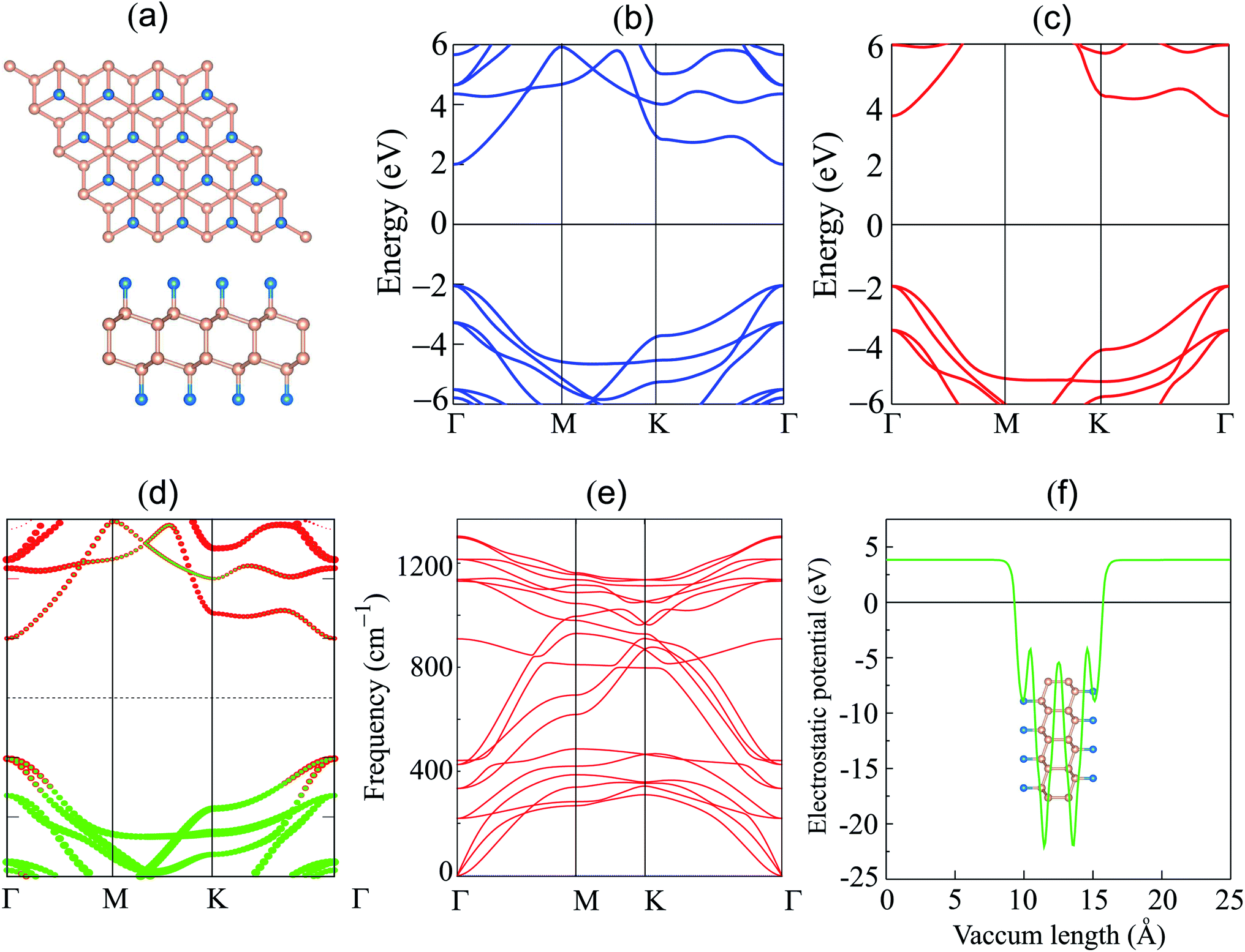 | ||
| Fig. 1 (a) Atomic structure; band structure given by (b) PBE and (c) HSE06 calculations, (d) weighted band structure; (e) phonon dispersion; and (f) electrostatic potential of the F-diamane-like C4F2 monolayer. Red and green balls in figure (d) represent the contributions of carbon and fluorine atoms, respectively. | ||
Now, we construct the atomic structures of the graphene/C4F2 vdW heterostructure by placing graphene on top of the C4F2 layer. The same lattice parameter of graphene (2.46 Å) and C4F2 (2.54 Å) gives rise to a small lattice mismatch of about 2% in the graphene/C4F2 vdW heterostructure. The optimized atomic structure of the graphene/C4F2 vdW heterostructure for different stacking configurations, namely SC-I, SC-II, SC-III and SC-IV are depicted in Fig. 3. The equilibrium interlayer distance between graphene and the topmost layer of the C4F2 layer is defined by D as shown in Fig. 2. The interlayer distance for all stacking configurations is calculated to be 3.35 Å. This finding demonstrates that the structural properties of the graphene/C4F2 vdW heterostructure are insensitive to the stacking configuration. Furthermore, we find that this value of the interlayer distance is the same as that of graphite65 and other graphene-based vdW heterostructures.56,66–70 This finding suggests that the graphene/C4F2 vdW heterostructure is mainly contributed by weak vdW interactions. Such vdW interactions keep the system stable and can be obtained in future by common methods such as CVD. Furthermore, it should be noted that the weak vdW interactions between graphene and the F-diamane-like C4F2 monolayer keeps the graphene/C4F2 vdWH stable and makes the graphene surface flat. However, in reality the graphene surface may be corrugated when it is deposited on the C4F2 monolayer. The surface corrugation may affect the change in the barrier height of the contact types. However, we believe that the surface corrugation does not change the band shapes and contact types of vdWHs.
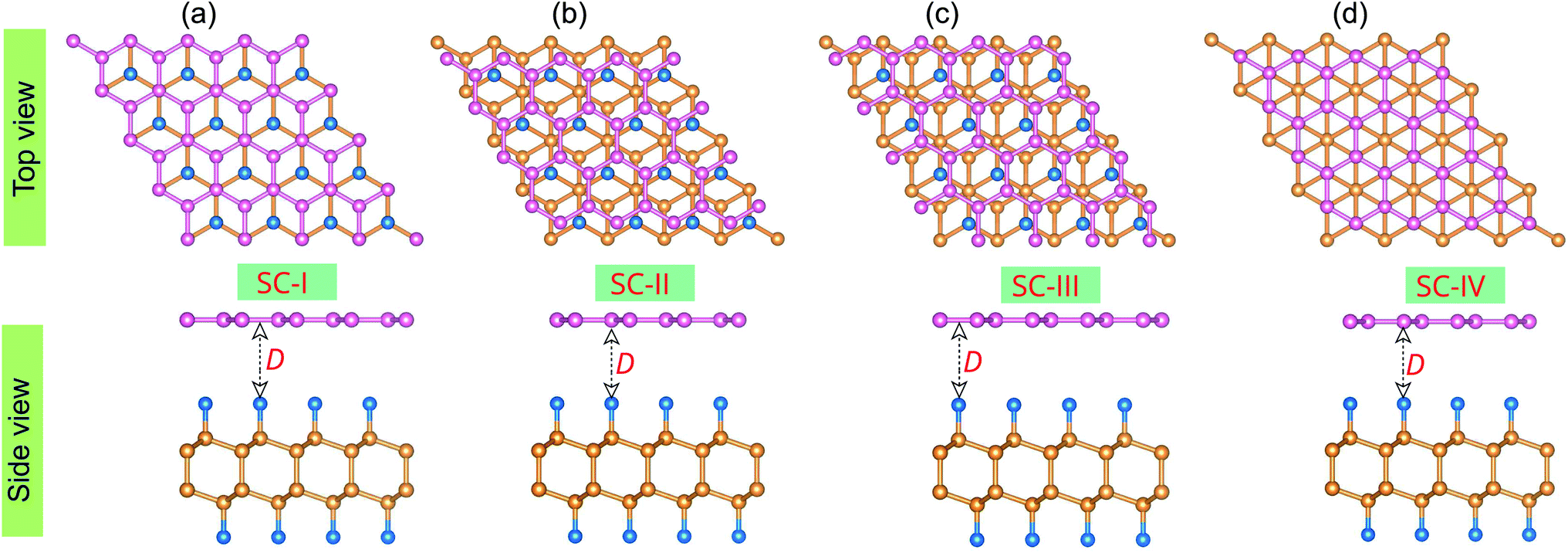 | ||
| Fig. 2 Top and side views of the optimized atomic structures of the graphene/C4F2 vdW heterostructures for different stacking configurations, (a) SC-I, (b) SC-II, (c) SC-III and (d) SC-IV. Pink, blue and orange balls represent carbon atoms in the graphene layer, fluorine and carbon atoms in the C4F2 layer, respectively. D stands for the equilibrium interlayer distance in the vdW heterostructure. | ||
To confirm the stability of such a heterostructure, we calculate the binding energy as follows:
 | (1) |
The projected band structures of the graphene/C4F2 vdW heterostructure for all stacking configurations are illustrated in Fig. 3. One can observe that the electronic band structure of the vdW heterostructure is the combination of those of the isolated constituent graphene and C4F2 monolayers. The reason of such a combination is due to the weak vdW interactions between graphene and C4F2 monolayers. Moreover, such band structures demonstrate that the stacking configurations do not affect the electronic properties of the heterostructure. Graphene maintains the metallic characteristic of a Dirac cone at the k point. While, the F-diamane-like C4F2 layer is the semiconductor with a direct band gap of 3.90/5.53 eV for PBE and HSE06 calculations for all stacking configurations. The contributions of each atom in the graphene/C4F2 vdW heterostructure for different stacking configurations are depicted in Fig. S2 ESI.† One can find that the Dirac cone around the Fermi level for all stacking configurations originates from the carbon atoms of the graphene layer. Interestingly, the band gap of the isolated F-diamane-like C4F2 layer is still smaller than that of the freestanding monolayer. This finding suggests that the graphene/C4F2 heterostructure may have a stronger optical absorption than that of its constituent monolayers.
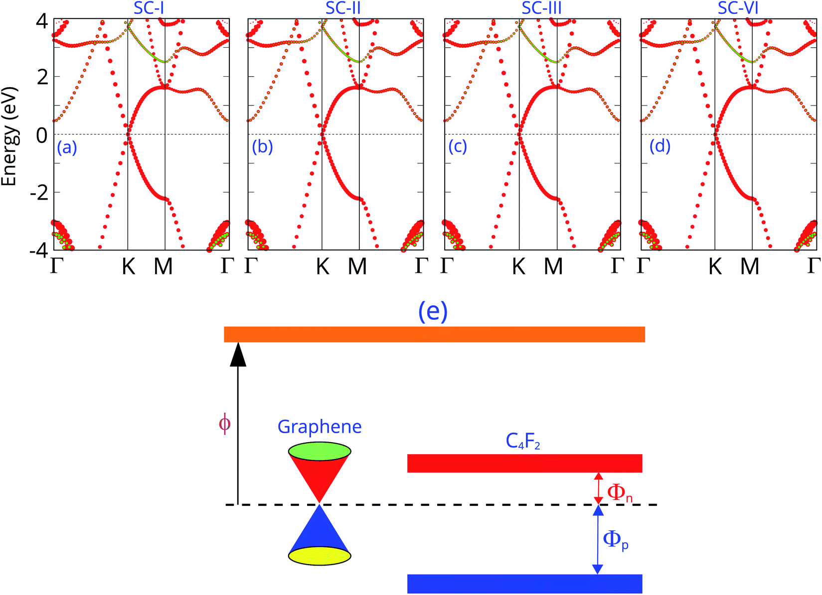 | ||
| Fig. 3 Projected band structures of the graphene/C4F2 vdW heterostructure for different stacking configurations of (a) SC-I, (b) SC-II, (c) SC-III and (d) SC-IV. Red and green balls represent the contributions of carbon and fluorine atoms, respectively. (e) Band diagram of the graphene/C4F2 vdW heterostructure. | ||
More interestingly, the contact between metallic graphene and the semiconducting C4F2 monolayer gives rise to the formation of metal–semiconductor contact, which is a crucial component of high-performance electronic and optoelectronic devices. Depending on the position of the VBM and CBM of semiconducting C4F2 relative to the Fermi level of metallic graphene, the graphene/C4F2 heterostructure may form either Schottky contact or ohmic contact. The schematic diagram of the graphene/C4F2 heterostructure is illustrated in Fig. 3(e), indicating that the graphene/C4F2 heterostructure forms the Schottky contact. The Schottky contact is mainly characterized by an energy barrier, namely the Schottky barrier height (SBH). Regarding the Schottky–Mott rule,71,72 the n-type SBH (Φn) and p-type (Φp) can be calculated as: Φn = ECBM − EF and Φp = EF − ECBM. The Φn and Φp are calculated to be 0.46/1.03 eV and 3.43/4.50 eV, given by PBE and HSE06 methods, respectively. This finding demonstrates that the graphene/C4F2 heterostructure exhibits an n-type Schottky contact for both PBE and HSE06 methods.
Furthermore, the graphene/C4F2 heterostructure is always subjected to an electric field when used as a component of electronic and optoelectronic devices. Therefore, it is important to check the effect of an external electric field on the electronic properties and contact types of the graphene/C4F2 heterostructure. The schematic model of applying an external electric field is depicted in Fig. 4(a). The electric field, pointing from the C4F2 monolayer graphene is defined as a positive direction. The change in the band gap as well as the SBH of the Schottky contact is illustrated in Fig. 4(b). One can find that in the presence of the positive electric field, ranging from 0 to +3 V nm−1, the Φn increases, while the Φp decreases accordingly. The change of the SBH of the graphene/C4F2 heterostructure under the positive electric field is almost linear. With the range of the positive electric field from 0 to +3 V nm−1, the Φn is still smaller than the Φp, indicating that the n-type Schottky contact is maintained in the graphene/C4F2 heterostructure. On the other hand, when the negative electric field is applied, the Φn decreases, while the Φp increases. At the critical negative electric field of −3 V nm−1, the Φn has already fallen to nearly zero, indicating a transformation from n-type Schottky contact to n-type ohmic contact.
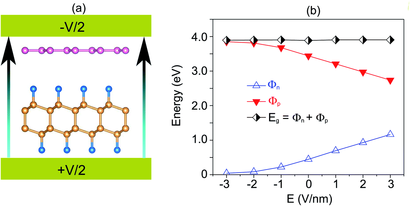 | ||
| Fig. 4 (a) Schematic diagram and (b) the variation of SBH, of the graphene/C4F2 heterostructure under an external electric field. | ||
The projected band structures of the graphene/C4F2 heterostructure under an electric field are plotted to provide a better understanding of the change in the electronic properties, as depicted in Fig. 5. One can see that when the positive electric field is applied, the VBM of the semiconducting C4F2 layer moves toward the Fermi level, while its CBM comes upward from the Fermi level. Such shifts cause the change in the Φn and Φp as we have discussed above. When the negative electric field is applied, the CBM is shifted downward to the Fermi level, while the VBM is moved far from the Fermi level. At the negative electric field of −3 V nm−1, the CBM of the semiconducting C4F2 layer crosses the Fermi level, suggesting a transformation from Schottky contact to an ohmic one. The nature of the change of band types of vdWH can be described by the change in the PFOS of all atoms, as depicted in Fig. S3 of the ESI.† All aforementioned discussions demonstrate that an external electric field gives rise not only to a change in the SBH, but also to a transition from Schottky to ohmic contact. Our findings reveal the potential of the graphene/C4F2 heterostructure as a tunable hybrid material with strong potential in electronic applications.
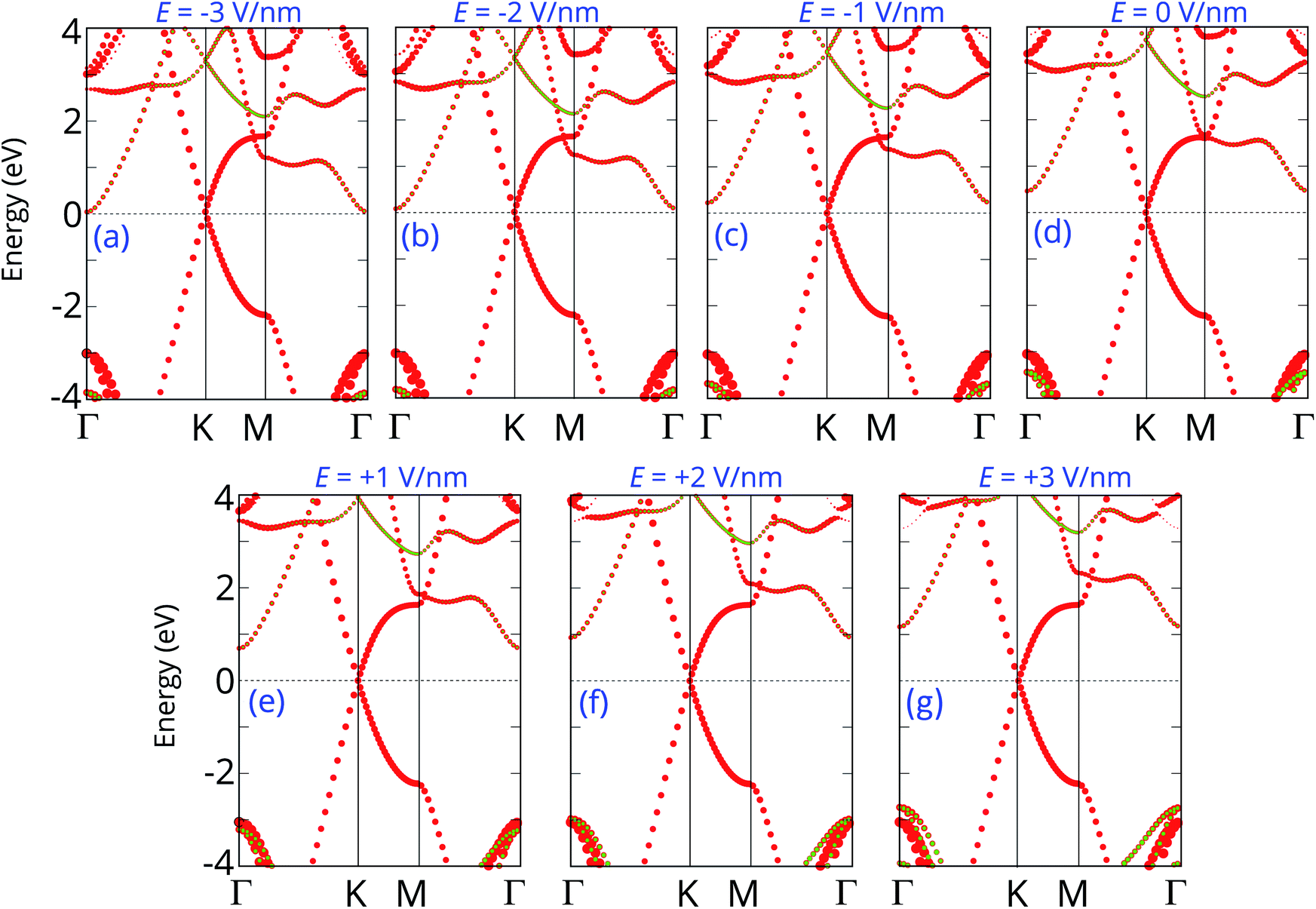 | ||
| Fig. 5 Projected band structures of graphene/C4F2 heterostructure under different electric field of (a) E = −3 V nm−1, (b) E = −2 V nm−1, (c) E = −1 V nm−1, (d) E = 0 V nm−1, (e) E = 1 V nm−1, (f) E = 2 V nm−1 and (g) E = 3 V nm−1. Red and green circles represent the contribution of C and F atoms, respectively. | ||
4 Conclusions
In summary, we have performed first-principles calculations to study the structural and electronic properties of the graphene/C4F2 heterostructure as well as the contact types and the effect of an external electric field. The graphene/C4F2 heterostructure is mainly characterized by weak vdW interactions with the interlayer distance of 3.35 Å and the binding energy of −45.32 meV per C atom for the most energetically favorable stacking configuration. The formation of the graphene/C4F2 heterostructure gives rise to a decrease in the band gap of semiconducting C4F2 layer and tends to the formation of the n-type Schottky contact with an SBH of 0.46/1.03 eV given by the PBE/HSE06 method. Both the contact type and SBH of the graphene/C4F2 heterostructure can be modified by applying an external electric field, which gives rise to the transformation from a Schottky contact to an ohmic one, and tends to a variation in the SBH. Our findings reveal the potential of the graphene/C4F2 heterostructure as a tunable hybrid material with strong potential in electronic applications.Conflicts of interest
There are no conflicts to declare.References
- J. Shen, Y. He, J. Wu, C. Gao, K. Keyshar, X. Zhang, Y. Yang, M. Ye, R. Vajtai and J. Lou, et al., Nano Lett., 2015, 15, 5449–5454 CrossRef CAS PubMed
.
- J. Kim, S. Kwon, D.-H. Cho, B. Kang, H. Kwon, Y. Kim, S. O. Park, G. Y. Jung, E. Shin and W.-G. Kim, et al., Nat. Commun., 2015, 6, 1–9 Search PubMed
- N. Mounet, M. Gibertini, P. Schwaller, D. Campi, A. Merkys, A. Marrazzo, T. Sohier, I. E. Castelli, A. Cepellotti and G. Pizzi, et al., Nat. Nanotechnol., 2018, 13, 246–252 CrossRef CAS PubMed
- Z. Cai, B. Liu, X. Zou and H.-M. Cheng, Chem. Rev., 2018, 118, 6091–6133 CrossRef CAS PubMed
- J. Yu, J. Li, W. Zhang and H. Chang, Chem. Sci., 2015, 6, 6705–6716 RSC
- Y.-L. Hong, Z. Liu, L. Wang, T. Zhou, W. Ma, C. Xu, S. Feng, L. Chen, M.-L. Chen and D.-M. Sun, et al., Science, 2020, 369, 670–674 CrossRef CAS PubMed
- K. S. Novoselov, A. K. Geim, S. V. Morozov, D.-e. Jiang, Y. Zhang, S. V. Dubonos, I. V. Grigorieva and A. A. Firsov, Science, 2004, 306, 666–669 CrossRef CAS PubMed
- S. Manzeli, D. Ovchinnikov, D. Pasquier, O. V. Yazyev and A. Kis, Nat. Rev. Mater., 2017, 2, 1–15 Search PubMed
- W. Choi, N. Choudhary, G. H. Han, J. Park, D. Akinwande and Y. H. Lee, Mater. Today, 2017, 20, 116–130 CrossRef CAS
- A. Carvalho, M. Wang, X. Zhu, A. S. Rodin, H. Su and A. H. C. Neto, Nat. Rev. Mater., 2016, 1, 1–16 Search PubMed
- H. Liu, A. T. Neal, Z. Zhu, Z. Luo, X. Xu, D. Tománek and P. D. Ye, ACS Nano, 2014, 8, 4033–4041 CrossRef CAS PubMed
- B. Anasori, M. R. Lukatskaya and Y. Gogotsi, Nat. Rev. Mater., 2017, 2, 1–17 Search PubMed
- J. Pang, R. G. Mendes, A. Bachmatiuk, L. Zhao, H. Q. Ta, T. Gemming, H. Liu, Z. Liu and M. H. Rummeli, Chem. Soc. Rev., 2019, 48, 72–133 RSC
- L. Zhang, Z. Yang, T. Gong, R. Pan, H. Wang, Z. Guo, H. Zhang and X. Fu, J. Mater. Chem. A, 2020, 8, 8813–8830 RSC
- R. Li, Y. Cheng and W. Huang, Small, 2018, 14, 1802091 CrossRef PubMed
- Z. Lin, C. Wang and Y. Chai, Small, 2020, 16, 2003319 CrossRef CAS PubMed
- X. Wang, Z. Song, W. Wen, H. Liu, J. Wu, C. Dang, M. Hossain, M. A. Iqbal and L. Xie, Adv. Mater., 2019, 31, 1804682 CrossRef CAS PubMed
- S. Yu, X. Wu, Y. Wang, X. Guo and L. Tong, Adv. Mater., 2017, 29, 1606128 CrossRef PubMed
- F. Schwierz, Nat. Nanotechnol., 2010, 5, 487–496 CrossRef CAS PubMed
- S. Ahmed and J. Yi, Nano-Micro Lett., 2017, 9, 1–23 CrossRef PubMed
- D. Pierucci, H. Henck, Z. Ben Aziza, C. H. Naylor, A. Balan, J. E. Rault, M. G. Silly, Y. J. Dappe, F. Bertran and P. Le Fèvre, et al., ACS Nano, 2017, 11, 1755–1761 CrossRef CAS PubMed
- D. Wang, X.-B. Li and H.-B. Sun, Nano Lett., 2021, 21, 6298–6303 CrossRef CAS PubMed
- H.-P. Komsa, J. Kotakoski, S. Kurasch, O. Lehtinen, U. Kaiser and A. V. Krasheninnikov, Phys. Rev. Lett., 2012, 109, 035503 CrossRef PubMed
- P. Luo, F. Zhuge, Q. Zhang, Y. Chen, L. Lv, Y. Huang, H. Li and T. Zhai, Nanoscale Horiz., 2019, 4, 26–51 RSC
- Y. Zhao, S. Ippolito and P. Samori, Adv. Opt. Mater., 2019, 7, 1900286 CrossRef
- X. Chen and A. R. McDonald, Adv. Mater., 2016, 28, 5738–5746 CrossRef CAS PubMed
- Z. Liu, S. P. Lau and F. Yan, Chem. Soc. Rev., 2015, 44, 5638–5679 RSC
- J. Padilha, A. Fazzio and A. J. da Silva, Phys. Rev. Lett., 2015, 114, 066803 CrossRef CAS PubMed
- Y. Liu, Y. Huang and X. Duan, Nature, 2019, 567, 323–333 CrossRef CAS PubMed
- S. Das, J. A. Robinson, M. Dubey, H. Terrones and M. Terrones, Annu. Rev. Mater. Res., 2015, 45, 1–27 CrossRef CAS
- S. Fan, Q. A. Vu, M. D. Tran, S. Adhikari and Y. H. Lee, 2D Mater., 2020, 7, 022005 CrossRef CAS
- A. R. Muniz and D. Maroudas, J. Phys. Chem. C, 2013, 117, 7315–7325 CrossRef CAS
- A. R. Muniz and D. Maroudas, Phys. Rev. B: Condens. Matter Mater. Phys., 2012, 86, 075404 CrossRef
- A. R. Muniz and D. Maroudas, J. Appl. Phys., 2012, 111, 043513 CrossRef
- M. Sun, J.-P. Chou, A. Hu and U. Schwingenschlogl, Chem. Mater., 2019, 31, 8129–8135 CrossRef CAS
- P. V. Bakharev, M. Huang, M. Saxena, S. W. Lee, S. H. Joo, S. O. Park, J. Dong, D. C. Camacho-Mojica, S. Jin and Y. Kwon, et al., Nat. Nanotechnol., 2020, 15, 59–66 CrossRef CAS PubMed
- X. Chen, M. Dubois, S. Radescu, A. Rawal and C. Zhao, Carbon, 2021, 175, 124–130 CrossRef CAS
- T. Cheng, Z. Liu and Z. Liu, J. Mater. Chem. C, 2020, 8, 13819–13826 RSC
- H. Shu, J. Mater. Chem. C, 2021, 9, 4505–4513 RSC
- H. Shu, Phys. Chem. Chem. Phys., 2021, 23, 18951–18957 RSC
- R. Frisenda, E. Navarro-Moratalla, P. Gant, D. P. De Lara, P. Jarillo-Herrero, R. V. Gorbachev and A. Castellanos-Gomez, Chem. Soc. Rev., 2018, 47, 53–68 RSC
- M. Huang, S. Li, Z. Zhang, X. Xiong, X. Li and Y. Wu, Nat. Nanotechnol., 2017, 12, 1148–1154 CrossRef CAS PubMed
- C. Zhang, C. Gong, Y. Nie, K.-A. Min, C. Liang, Y. J. Oh, H. Zhang, W. Wang, S. Hong and L. Colombo, et al., 2D Mater., 2016, 4, 015026 CrossRef
- Z. Cui, K. Ren, Y. Zhao, X. Wang, H. Shu, J. Yu, W. Tang and M. Sun, Appl. Surf. Sci., 2019, 492, 513–519 CrossRef CAS
- Y.-C. Lin, R. K. Ghosh, R. Addou, N. Lu, S. M. Eichfeld, H. Zhu, M.-Y. Li, X. Peng, M. J. Kim and L.-J. Li, et al., Nat. Commun., 2015, 6, 1–6 Search PubMed
- N. Huo, Y. Yang and J. Li, J. Semicond., 2017, 38, 031002 CrossRef
- I. Shahid, S. Ahmad, N. Shehzad, S. Yao, C. V. Nguyen, L. Zhang and Z. Zhou, Appl. Surf. Sci., 2020, 523, 146483 CrossRef CAS
- Y. Zheng, Y. Chen, B. Gao, B. Lin and X. Wang, Engineering, 2021, 7(7), 991–1001 CrossRef CAS
- P. Wang, J. Meng, J. Huang, J.-j. Wang and Q.-x. Li, Chin. J. Chem. Phys., 2019, 32, 431 CrossRef CAS
- W. Zhang, Y. Zeng, N. Xiao, H. H. Hng and Q. Yan, J. Mater. Chem., 2012, 22, 8455–8461 RSC
- J. Tan, A. Avsar, J. Balakrishnan, G. Koon, T. Taychatanapat, E. O’Farrell, K. Watanabe, T. Taniguchi, G. Eda and A. Castro Neto, et al., Appl. Phys. Lett., 2014, 104, 183504 CrossRef
- J. Wang, X. Mu, M. Sun and T. Mu, Appl. Mater. Today, 2019, 16, 1–20 CrossRef
- P. Solís-Fernández, M. Bissett and H. Ago, Chem. Soc. Rev., 2017, 46, 4572–4613 RSC
- Z. B. Aziza, H. Henck, D. Di Felice, D. Pierucci, J. Chaste, C. H. Naylor, A. Balan, Y. J. Dappe, A. C. Johnson and A. Ouerghi, Carbon, 2016, 110, 396–403 CrossRef
- C. V. Nguyen, M. Idrees, H. V. Phuc, N. N. Hieu, N. T. Binh, B. Amin and T. V. Vu, Phys. Rev. B, 2020, 101, 235419 CrossRef CAS
- C. V. Nguyen, Phys. Rev. B, 2021, 103, 115429 CrossRef CAS
- Z. B. Aziza, D. Pierucci, H. Henck, M. G. Silly, C. David, M. Yoon, F. Sirotti, K. Xiao, M. Eddrief and J.-C. Girard, et al., Phys. Rev. B, 2017, 96, 035407 CrossRef
- G. Kresse and J. Furthmüller, Comput. Mater. Sci., 1996, 6, 15–50 CrossRef CAS
- P. Giannozzi, S. Baroni, N. Bonini, M. Calandra, R. Car, C. Cavazzoni, D. Ceresoli, G. L. Chiarotti, M. Cococcioni and I. Dabo, et al., J. Phys.: Condens. Matter, 2009, 21, 395502 CrossRef PubMed
- P. Giannozzi, O. Andreussi, T. Brumme, O. Bunau, M. B. Nardelli, M. Calandra, R. Car, C. Cavazzoni, D. Ceresoli and M. Cococcioni, et al., J. Phys.: Condens. Matter, 2017, 29, 465901 CrossRef CAS PubMed
- J. P. Perdew, K. Burke and M. Ernzerhof, Phys. Rev. Lett., 1996, 77, 3865 CrossRef CAS PubMed
- G. Kresse and D. Joubert, Phys. Rev. B: Condens. Matter Mater. Phys., 1999, 59, 1758 CrossRef CAS
- S. Grimme, J. Comput. Chem., 2006, 27, 1787–1799 CrossRef CAS PubMed
- C.-H. Hu, P. Zhang, H.-Y. Liu, S.-Q. Wu, Y. Yang and Z.-Z. Zhu, J. Phys. Chem. C, 2013, 117, 3572–3579 CrossRef CAS
- M. Hasegawa, K. Nishidate and H. Iyetomi, Phys. Rev. B: Condens. Matter Mater. Phys., 2007, 76, 115424 CrossRef
- H. Henck, Z. Ben Aziza, D. Pierucci, F. Laourine, F. Reale, P. Palczynski, J. Chaste, M. G. Silly, F. m. c. Bertran, P. Le Fèvre, E. Lhuillier, T. Wakamura, C. Mattevi, J. E. Rault, M. Calandra and A. Ouerghi, Phys. Rev. B, 2018, 97, 155421 CrossRef CAS
- M. Sun, J.-P. Chou, Q. Ren, Y. Zhao, J. Yu and W. Tang, Appl. Phys. Lett., 2017, 110, 173105 CrossRef
- M. Sun, J.-P. Chou, J. Yu and W. Tang, J. Mater. Chem. C, 2017, 5, 10383–10390 RSC
- L. Lv, Y. Shen, Y. Ma, X. Gao, J. Liu, S. Wu, X. Wang, D. Gong and Z. Zhou, J. Phys. D: Appl. Phys., 2021, 54, 155104 CrossRef CAS
- X. Gao, Y. Shen, Y. Ma, S. Wu and Z. Zhou, Carbon, 2019, 146, 337–347 CrossRef CAS
- R. T. Tung, Appl. Phys. Rev., 2014, 1, 011304 Search PubMed
- Y. Liu, J. Guo, E. Zhu, L. Liao, S.-J. Lee, M. Ding, I. Shakir, V. Gambin, Y. Huang and X. Duan, Nature, 2018, 557, 696–700 CrossRef CAS PubMed
Footnote |
| † Electronic supplementary information (ESI) available. See DOI: 10.1039/d1ra06986a |
| This journal is © The Royal Society of Chemistry 2021 |