DOI:
10.1039/D1RA06940C
(Paper)
RSC Adv., 2021,
11, 37120-37130
Tunable formaldehyde sensing properties of palladium cluster decorated graphene†
Received
16th September 2021
, Accepted 12th November 2021
First published on 18th November 2021
Abstract
The ability to tune the adsorption strength of the targeted gas on sensing materials is crucial for sensing applications. By employing first-principles calculations the adsorption and sensing properties of HCHO on small Pdn (n = 1–6) cluster decorated graphene have been systematically investigated. The adsorption energy is found to depend on the size of the Pdn cluster and can be tuned in a wide range from −0.68 eV on Pd(111) to −1.98 eV on the Pd3/graphene system. We also find that the Pdn/graphene (n = 5 and 6) systems have an appropriate adsorption energy for HCHO gas sensing. The current–voltage curves are calculated by the non-equilibrium Green's function method for the two-probe nano-sensor devices along both the armchair and zigzag directions. The devices constructed with Pdn/graphene (n = 5 and 6), having the highest absolute response over 20% at small voltages, should be applicable for HCHO detection. This work provides a theoretical basis for exploring potential applications of metal cluster decorated graphene for gas sensing.
1. Introduction
Formaldehyde is one of the volatile organic compounds (VOCs) that is chronically and slowly emitted and evaporated from upholstery, carpeting, adhesives, wood and plate products, furniture, and lacquer which are widely used in house construction and decoration.1,2 Moreover, it is an essential ingredient of consumer goods, such as shampoos, soap, and detergents, and utilized in pharmacology and medicine because of its disinfection effect. Exposure in the circumstances of formaldehyde has been confirmed as a crucial cause of sick building syndrome (SBS) to humans and animals.2,3 The most common health detriment from formaldehyde is an irritation of the eyes, nose, throat, and skin mucous membrane, and with the increase in the formaldehyde concentration, nausea, cough, headache and other symptoms can appear. Under conditions of unusually high or prolonged exposure, formaldehyde is categorized as a mutagen and possible human carcinogen and teratogens.4–6 Therefore, efficient and convenient methods to detect formaldehyde have been strongly demanded for indoor and outdoor environmental measurement and control. The development of formaldehyde sensors is thought to be a desirable means for the gas monitoring because the gas sensors own the advantages of excellent selectivity, fast response, low time-consumption, simple operation, and real-time detection in situ condition.7–9
The graphene decorated by metal nanostructures has become promising materials for various applications, such as chemical sensors, electronic devices, energy storage and fuel cells.10,11 These materials have caught great scientific and technological interests.12–15 Recently, the graphene sheets functionalized with metal nanoparticles had shown to increase the selectivity, sensitivity, limit of detection, response, or an unio of these performances.16–19 Gutés et al.16 exploited an simple and easy-to-implement method of electroless deposition of Au nanoparticles to fabricate Au-decorated graphene sensor for H2S detecting in relatively fast response. Dong et al.17 developed a biosensor synthesized by assembling Au–Pd/graphene nanocomposites with high electroactive surface and electrical conductivity, which resulted in sensing toward H2O2 in cancer cell with a low detection limit, a good linear range, and a rapid response. Kumar et al.18 reported the fast response and recovery of H2 sensing of Pd–Pt alloy nanoparticle-graphene composite layers fabricated using chemical methods. Fan et al.19 found that Au nanoparticles decorated graphene could enhanced the NO2 detecting with fast response, good reversibility and mechanical stability, and high sensitivity. It had demonstrated that palladium nanoparticles could be the very effective oxidation catalysts and electrochemical sensors for formaldehyde.12,13,20–23 The formaldehyde detecting properties of single-walled carbon nanotube hybridized with Pd were investigated by density-functional theory calculations.22 These researches indicated that metal nanoparticles decorated graphene shows a great potential for applying to the gas sensing and catalysis.
In this paper, we investigate the HCHO absorption and sensing properties of Pdn (n = 1–6) clusters supported on graphene by using non-equilibrium Green's function (NEGF) method combined with the density-functional theory (DFT). We find that it is possible to adjust the adsorption strength of HCHO gas on Pdn (n = 1–6) clusters supported on graphene by changing the size of Pdn cluster. As increasing the size of Pd cluster the adsorption strength decreases and the adsorption energy approaches the value of −0.68 eV for the HCHO adsorption on Pd(111), which is beyond the low limit of targeted gas adsorption energy −0.8 eV required by good sensitivity.24 The geometries of Pdn nanoclusters supported on graphene for the both cases with and without HCHO adsorption are optimized, and the HCHO adsorption energies are calculated. The two-probe nano-sensor devices consisted of the left/right electrodes and the central scattering region are constructed, and the current–voltage curves and sensor responses are simulated. The results indicate that the systems of Pdn (n = 5 and 6) clusters supported on graphene having the proper adsorption energy and a large enough response at low bias voltages are promising for HCHO sensing applications.
2. Computational details
All the structural optimizations and electronic property calculations are performed by using the Vienna Ab initio Simulation Package (VASP),25,26 adopting the generalized gradient approximation (GGA) in the Perdew, Burke and Ernzernhof (PBE) functional27 for exchange-correlation potential and the projector augmented wave (PAW) method28 to describe the electron–ion interaction. A conjugate-gradient (CG) algorithm is performed to relax all the ions until the force acting on each ion is less than 0.01 eV Å−1. The graphene is modelled by a (4 × 4) supercell containing 32 carbon atoms and a 15 Å thick vacuum in the z direction which is perpendicular to the graphene surface. A large (5 × 5) supercell is also used for testing the lateral interaction imposed by the periodic boundary conditions and we find that the lateral interaction in the (4 × 4) graphene supercell model is negligible. The vacuum thickness is large enough to avoid interactions with the adjacent cells due to the periodic boundary conditions enforced in the calculations. The following electronic states are chosen as the valence electron configurations in the pseudopotential description of the system: 1s for H, 2s2p for C and O, and 4d5s for Pd. A semiempirical DFT-D2 (ref. 29) correction is employed to describe van der Waals interactions between the graphene substrate and gas molecule. The more sophisticated D3 correction method has also tested in our calculations and the results show that the HCHO adsorptions on Pdn/graphene become slightly weaker by about 0.1 eV. The plane-wave cutoff energy is set to be 500 eV, and a Gaussian smearing for the occupation of the electronic levels has been adopted in all DFT simulations. The Brillouin zone integrations are performed with 5 × 5 × 1 and 15 × 15 × 1 Monkhorst–Pack meshes for atomic relaxations and electronic structure calculations, respectively. The theoretical C–C bond length in graphene is 1.43 Å, which is in excellent agreement with the previous work.30 For HCHO adsorption on the Pdn/graphene substrate, the charge transfer Δq is obtained based on the Bader charge analysis.31,32 Positive Δq means the electron gain of adsorbed gas molecule from the substrate.
The formaldehyde adsorption energy on the Pdn/graphene substrate is calculated as follows:
| | |
Eads = EHCHO–Pdn/Gr − EPdn/Gr − EHCHO
| (1) |
where
EHCHO–Pdn/Gr,
EPdn/Gr and
EHCHO represent the total energies of the system of HCHO molecule adsorbed on Pd
n/graphene substrate, the Pd
n cluster loaded on graphene substrate and an isolated HCHO molecule, respectively. A negative
Eads means that the adsorption is exothermic.
The electronic transport properties are investigated by Nanodcal,33,34 which employs the non-equilibrium Green's function technique with the Keldysh formalism in combination with DFT.35,36 The GGA-PBE functional27 is adopted as the exchange-correlation potential and double ζ-plus basis (DZP) is employed for the basis set. The real space mesh cutoff energy is 100 Ha, and the Brillouin zone samplings are represented by Monkhorst–Pack mesh of 1 × 15 × 1 and 1 × 15 × 100 k-points for the electrode and central region of the two-probe geometry, respectively.
The electronic transmission function through the device is obtained by the Landauer formula,37 as follows
| | |
T(E,Vb) = Tr[ΓL(E)GR(E)ΓR(E)GA(E)]
| (2) |
where
GR/A is the retarded/advanced Green's function in the central scattering region, and
ΓL/R is the coupling matrix between the central zone and the left/right leads.
33 The transmission around the Fermi energy at the equilibrium state is
T(
E,
V) =
Tr[
ΓLGRΓRGA], which represents the probability that an electron with the energy
E transmits from the left electrode into the right one. For non-equilibrium transport properties, the electrochemical potentials
μL/R =
μ ±
eVb/2, where
μ and
Vb are the Fermi level and the applied bias, are applied to the left and right electrodes, respectively. The current through the device is given using the Landauer–Büttiker equation,
38| | |
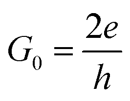
I(Vb) = G0∫T(E,Vb)[f(E − μL) − f(E − μR)]dE
| (3) |
where the

is the unit of the quantum conductance and
f(
E −
μL/R) is the Fermi–Dirac distribution function of the left/right electrode.
3. Results and discussion
3.1 Geometries of free-standing and graphene-supported Pdn clusters
The free-standing Pdn clusters with 2–6 atoms are relaxed and the optimized structures are displayed in Fig. 1. As shown in Fig. 1, the average Pd–Pd bond length of a Pdn cluster increases with increasing its cluster size and gradually approaches to the bond length of 2.75 Å for the Pd bulk phase. The bond length results are in good agreement with those values in literature.39 For the Pdn (n ≥ 4) clusters the three-dimensional (3D) structure is energetically more favorable than the flat one.
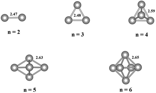 |
| | Fig. 1 Optimized geometries of free-standing Pdn (n = 2–6) clusters. The average Pd–Pd bond lengths (in Å) are given for the clusters. Gray balls represent Pd atoms. | |
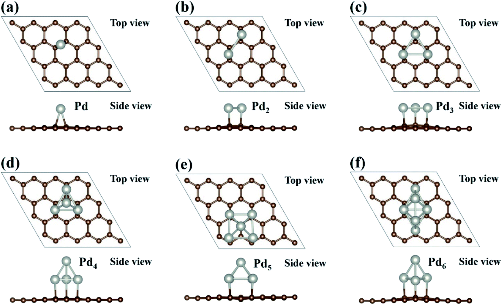
There are multiple ways to build a Pdn cluster loaded on the graphene substrate. We have employed two different approaches to search for the most stable atomic configuration of a Pdn cluster loaded on graphene. In the first approach, the optimized Pdn clusters as shown in Fig. 1 are placed on the graphene surface in various orientations, and in the second approach the Pdn/graphene structure is built by adding Pd atoms one by one to previously optimized Pdn − 1/graphene at some possible positions. After relaxing all the atomic configurations, the most stable structures of Pdn/graphene are shown in Fig. 2 and the structural files are also provided as ESI.† Their structural and energetic results are presented in Table 1. In Table 1, dPd–Pd and dPd–C(Gr) are the average Pd–Pd bond length in the Pdn clusters and the shortest distance between the Pd atom and the C atom of graphene, respectively. A single Pd atom on the graphene surface prefers to occupy the bridge site as shown in Fig. 2(a). Similar to the single Pd atom case, for the Pdn (n = 2 & 3) clusters all Pd atoms prefer to occupy the bridge sites. For a larger Pdn (n = 4–6) cluster it tends to have a 3D structure. The supported Pd5 and Pd6 clusters have very different atomic configurations from those free-standing ones, while the supported Pdn (n = 2–4) clusters have the same shape as the free-standing ones although their average Pd–Pd bond lengths are enlarged. The Pdn (n = 4–6) clusters have the shapes of tetrahedron, hexahedron and octahedron, respectively.39 The Pd–Pd bond lengths in the Pdn clusters on the graphene surface vary in an irregular way and appear to oscillate as shown in Table 1, which is a general phenomenon well known for isolated metal clusters.40 The distances dPd–C(Gr) between the Pd atom and the C atom of graphene are also larger for the large Pdn (n = 4–6) clusters compared to those for the small Pdn (n = 1–3) clusters, as shown in Table 1. This may be associated with the 2D–3D structure transformation of Pdn clusters. Overall, our final stable Pdn structures supported on the graphene substrate are very close to those obtained in ref. 39 and 40.
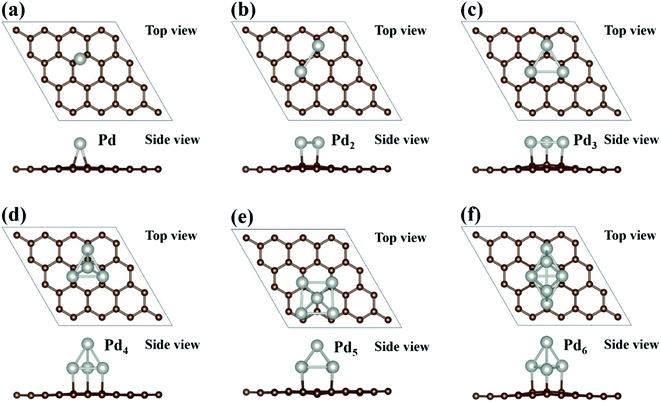 |
| | Fig. 2 The most stable configurations of Pdn (n = 1–6) clusters supported on graphene are presented in (a–f). Brown and sliver balls represent the C and Pd atoms, respectively. | |
Table 1 Optimized geometric and energetic results of Pdn (n = 1–6) clusters supported on graphene. The average Pd–Pd bond length dPd–Pd in Pdn clusters and the average Pd–C bond length dPd–C(Gr) between Pd atom and adjacent C atom in graphene are also presented in the table
| Clusters |
dPd–Pd (Å) |
dPd–C(Gr) (Å) |
Eb (eV) |
Eint (eV) |
| Pd1 |
— |
2.18 |
−1.10 |
−1.10 |
| Pd2 |
2.71 |
2.20 |
−1.35 |
−1.44 |
| Pd3 |
2.75 |
2.22 |
−1.52 |
−0.79 |
| Pd4 |
2.63 |
2.34 |
−1.85 |
−0.67 |
| Pd5 |
2.66 |
2.41 |
−1.94 |
−0.66 |
| Pd6 |
2.74 |
2.28 |
−2.07 |
−0.66 |
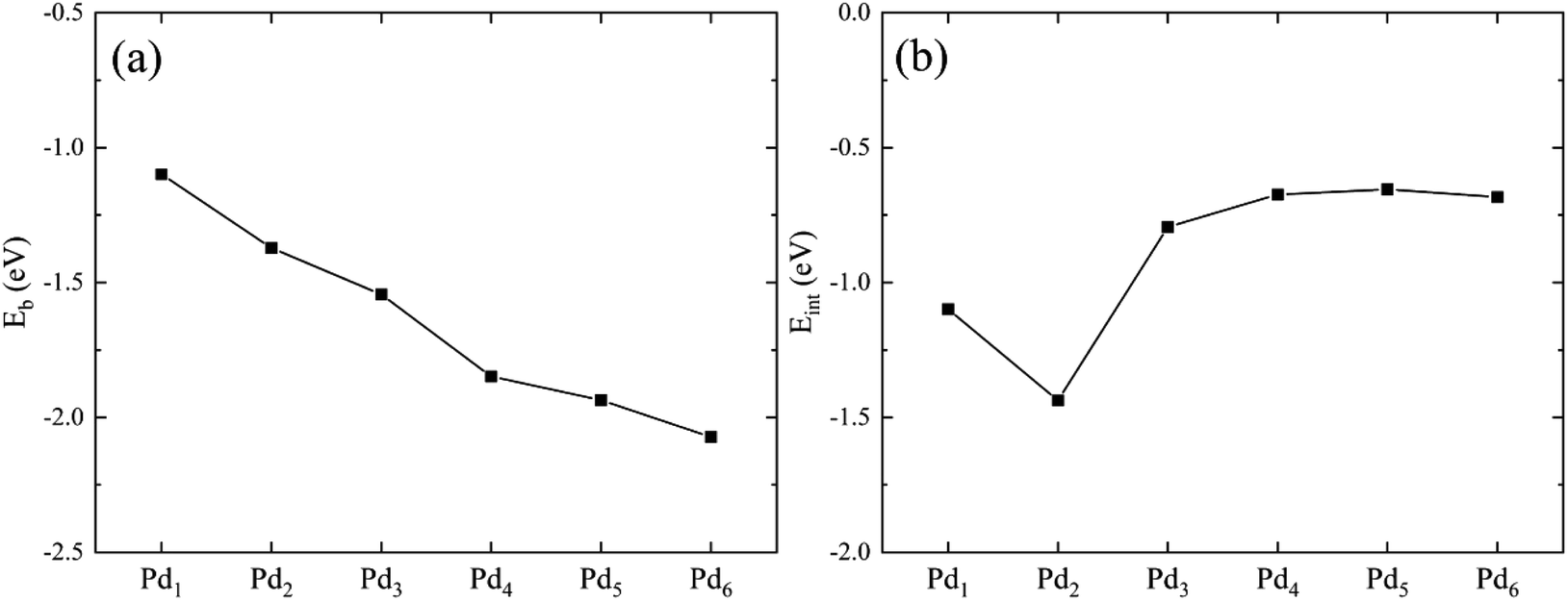
To evaluate the stability of a Pdn cluster loaded on graphene, the binding energy Eb is calculated as follows
| | |
Eb = [EPdn/Gr − n × EPd − EGr]/n
| (4) |
where
EPdn/Gr is same as it in
eqn (1),
EGr and
EPd are the energies of the graphene supercell and free Pd atom, respectively. The interaction energy between the Pd
n cluster and graphene is defined as
| | |
Eint = EPdn/Gr − EPdn − EGr
| (5) |
where
EPdn is the energy of the free-standing Pd
n cluster, and the others on the right side of the equation are same as those in
eqn (4). The interaction energy
Eint is to evaluate the interaction between the Pd
n cluster and the graphene substrate, while the binding energy
Eb represents the stability of the system,
i.e. the average formation energy per Pd atom.
We plot Eb and Eint as a function of the Pdn cluster size in Fig. 3. The binding energy is almost linearly dependent on the Pd cluster size. With increasing the cluster size, the cluster becomes more stable. The stability increase of the Pdn cluster supported on graphene is mainly attributed to the formation of Pd–Pd bonds. For example, for the Pd2 cluster the binding energy (per Pd atom) is 0.25 eV lower than that of Pd1 supported on graphene, which can be caused by the Pd–Pd bond formed in the cluster. For the interaction energy Eint in Fig. 3(b), it shows that the interaction between the Pdn cluster and graphene is stronger for the small Pdn (n = 1–3) cases relative to the large Pdn (n = 4–6) cases. The moderate interaction of about −0.66 eV for the large Pdn (n = 4–6) cases may explain their atomic structure changes and electron scattering effects upon HCHO adsorption, as discussed below. The interaction energy results are in agreement with the previous studies by Cabria et al.41 and Xiao et al.42
 |
| | Fig. 3 The binding energy Eb (a) and the interaction energy Eint between the Pdn cluster and the graphene substrate (b) as a function of the cluster size. | |
3.2 Formaldehyde adsorption on Pd(111) and Pdn/graphene
The formaldehyde adsorption on the Pd(111) surface is calculated, and the adsorption energy is defined as EPd(111)ads = EHCHO–Pd(111) − EPd(111) − EHCHO. EHCHO–Pd(111) is the total energy of a formaldehyde molecule adsorbed on the Pd(111) slab, and EPd(111) and EHCHO are the total energies of the Pd(111) slab and the isolated formaldehyde molecule, respectively. The slab model consisting of five Pd atomic layers and a vacuum thickness of 15 Å is constructed with the theoretical equilibrium lattice constant of 3.89 Å and a (3 × 3) surface supercell. The adsorbed HCHO and Pd atoms in the top three layers are allowed to relax, while the atoms in the bottom two layers are fixed at the bulk lattice sites. After full structure relaxation, the most stable absorption geometry is obtained, in which the carbonyl group of HCHO gas molecule is parallel to the Pd(111) surface and both the C and O atoms bond to Pd atoms with the bond lengths of 2.17 Å and 2.14 Å, respectively. The calculated adsorption energy Eads is −0.68 eV, which is at least 0.25 eV lower than those for different adsorption geometries, such as the one that only O atom is formed the bond with the Pd atom on the surface. The result is in good agreement with previous works.23,43,44
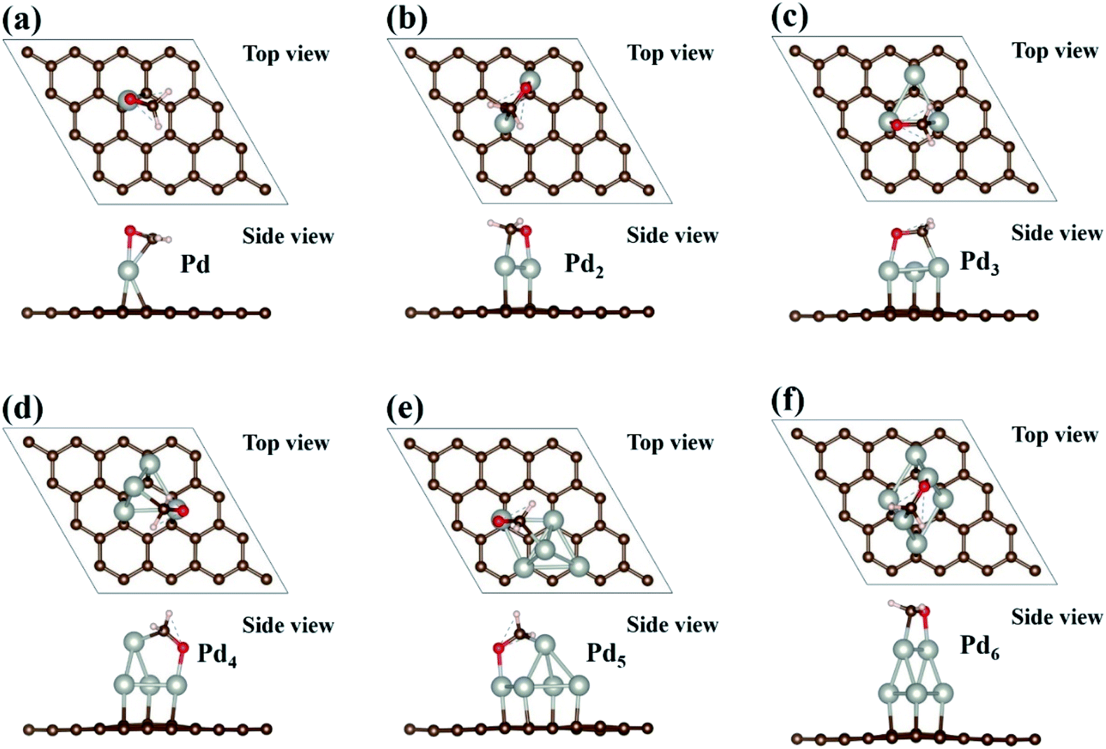
The adsorptions of HCHO molecule on the Pdn (n = 1–6) clusters supported on graphene have been investigated. The initial HCHO adsorption geometries are built by considering various possible orientations of the HCHO molecule and adsorption sites. We fully relax the initial HCHO adsorption structures and obtain the most stable adsorption atomic configuration for each case. The optimized atomic configurations and the corresponding adsorption energies are presented in Fig. 4 and Table 2. In Fig. 4, we can see that the adsorbed HCHO molecule is bonded to the Pdn clusters supported on graphene through both C and O atoms of HCHO molecule, which is similar to the HCHO adsorption on Pd(111).43 Moreover, the interaction of adsorbed HCHO molecule with the Pdn cluster can dramatically affect the atomic configurations of the Pdn clusters supported on graphene. For example, for the Pd1 case the Pd atom at the bridge site on graphene has been moved to the atop site upon HCHO adsorption, and the Pd atom in the top atomic layer of the Pd4 cluster moves away from the vertex site to the bridge site between two Pd atoms. For the Pd5 cluster the square base has been changed to the parallelogram shape, while for the Pd6 cluster two Pd atoms in the top atomic layer move to the bridge sites from the hollow sites upon HCHO adsorption. However, we hope that the Pdn clusters can resume their original atomic configurations in Fig. 2 after HCHO desorption and are applicable to HCHO detecting.
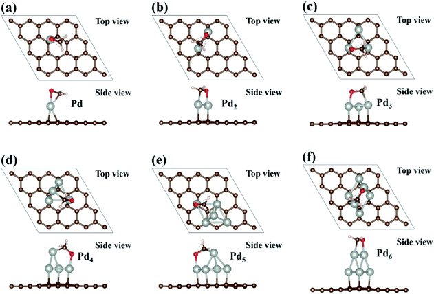 |
| | Fig. 4 Optimized geometries of Pdn (n = 1–6) cluster supported on graphene with HCHO adsorption are presented in (a–f). Brown, white, red and sliver balls represent the C, H, O and Pd atoms, respectively. | |
Table 2 Optimized atomic structures and adsorption energies of HCHO molecule absorbed on Pdn/graphene and Pd(111). The dC–O is the C–O bond length in the adsorbed HCHO molecule. The electron gains of the adsorbed HCHO molecule ΔqHCHO and graphene without HCHO adsorption ΔqGrap and with HCHO adsorption ΔqGrap (HCHO) are obtained by the Bader charge analysis, and the HCHO adsorption energies Eads are calculated according to eqn (1)
| Clusters |
dC–O (Å) |
ΔqHCHO |
ΔqGrap |
ΔqGrap (HCHO) |
Eads (eV) |
| Pd1 |
1.29 |
0.25 |
0.17 |
0.08 |
−1.42 |
| Pd2 |
1.32 |
0.36 |
0.24 |
0.19 |
−1.83 |
| Pd3 |
1.34 |
0.39 |
0.31 |
0.33 |
−1.98 |
| Pd4 |
1.33 |
0.36 |
0.26 |
0.29 |
−1.49 |
| Pd5 |
1.32 |
0.34 |
0.30 |
0.32 |
−1.17 |
| Pd6 |
1.31 |
0.32 |
0.30 |
0.31 |
−1.03 |
| Pd(111) |
1.32 |
0.26 |
— |
— |
−0.68 |
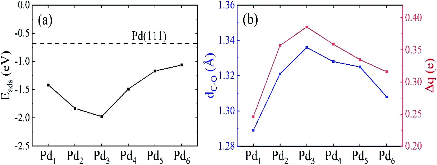
The HCHO adsorption energies on the Pdn clusters supported on graphene are plotted in Fig. 5. The HCHO adsorption becomes stronger from Pd1 to Pd3 clusters, and then becomes weaker when further increasing the size of the Pdn cluster. The strongest adsorption for the Pd3 cluster supported on graphene has the adsorption energy of −1.98 eV. The adsorption on the 3D Pdn clusters is weaker compared to those on the 2D Pdn clusters, and it gradually approaches the adsorption energy of −0.68 eV on Pd(111) as the size of Pdn cluster increases. This large adsorption energy difference of 1.30 eV between the adsorptions on the Pd3 cluster and Pd(111) makes it feasible to tune the HCHO adsorption strength on the Pdn cluster decorated graphene by adjusting its size. The adsorption strength on the Pdn (n = 5 and 6) cluster decorated graphene is in the proper adsorption energy range, implying their potential applications as HCHO sensors. The adsorption strength between the targeted gas and sensing materials is a key factor for sensor applications because it needs to balance the sensitivity and the recovery time. In a previous work,45 the authors investigated HCHO adsorption on Ti- and V-doped graphene and estimated the recovery times to be 10−3 s and 104 s corresponding to the adsorption energies of −1.12 eV and −1.94 eV, respectively. Therefore, in our previous work24 we suggested that the adsorption energy should be in the range of −0.8 to −1.2 eV in order to have a good balance between the sensitivity and the recovery time. From Fig. 5, we also find that there is a certain correlation between the adsorption energy and C–O bond length and charge transfer of HCHO molecule. That is that for the Pdn cluster system which has a larger C–O bond length and charge transfer, the HCHO adsorption is also stronger, and vice versa. For the Pd3 cluster, for instance, the HCHO adsorption is the strongest while it has the largest C–O bond length and charge transfer.
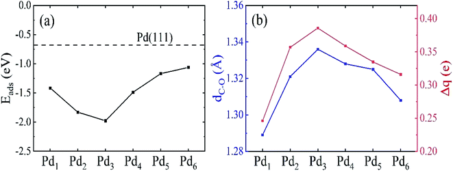 |
| | Fig. 5 (a) The HCHO adsorption energy on Pdn (n = 1–6) supported on graphene as a function of the cluster size. The dashed horizontal line in (a) represents the HCHO adsorption energy on Pd(111). (b) The C–O bond length dC–O and charge transfer Δq of the adsorbed HCHO molecule on Pdn/graphene. | |
Compared to the C–O bond length (1.21 Å) of isolated HCHO molecule, the C–O bond of the adsorbed HCHO molecule is enlarged as shown in Table 2 and Fig. 5. The charge transfers of adsorbed HCHO are all positive and it means that the HCHO molecule acts as electron acceptor to gain the electrons from the Pdn/graphene substrate. We plot the C–O bond length and the charge transfer as a function of the size of Pdn cluster in Fig. 5(b). As discussed in previous studies46 the C–O bond length of the adsorbed HCHO molecule on the Pdn/graphene substrate is closely correlated with its electron gain from the substrate. From Fig. 5, it confirms that there is a similar trend for both the C–O bond length and the electron gain of adsorbed HCHO molecule. With increasing the size of Pdn cluster, the C–O bond length and the electron gain of HCHO molecule first increase and then decrease. For the Pd3 cluster case, the C–O bond expands 0.13 Å compared to that of HCHO molecule in the gas phase. The corresponding charge transfer of 0.39e is also the largest. A large elongation of the C–O bond implies the bond strength is weakened, which may be caused by the large charge transfer and strong interaction between the molecule and the Pd cluster.
The charge density difference (CDD) is defined as Δρ = ρHCHO–Pdn/Gr − ρHCHO − ρPdn/Gr, where ρHCHO–Pdn/Gr is the charge density of the interacting system, ρHCHO and ρPdn/Gr are the charge densities of the isolated HCHO molecule and the Pdn/graphene substrate, respectively. The 3D iso-surfaces of CDD and the planar-average charge-density difference Δρ along the z axis are plotted in Fig. 6. The cyan and yellow areas of CDD denote the charge depletion and accumulation, respectively, and the iso-surface level is set to 0.002 e Å−3. Positive values of the planar-average Δρ indicate the electron gain at the z-axis transverse section. The adsorption of HCHO molecule onto Pdn/graphene can greatly change the charge distribution. Obviously, there is an electron accumulation between the O or C atom of HCHO and the Pd atom that it is bonded to. From the planar-average Δρ for the Pd2 and Pd3 cases, it can clearly see that the largest electron gain is located the middle region of the C–Pd and O–Pd bonds. The CCD results in Fig. 6 verify that the HCHO molecule gains electrons from the substrate, which is consistent with the Bader charge analyses.
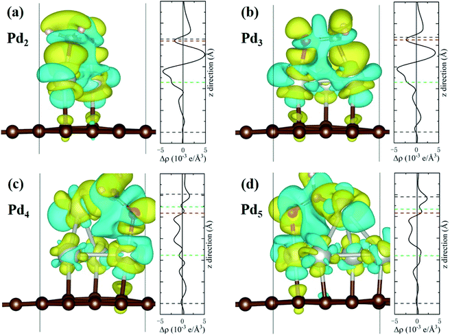 |
| | Fig. 6 The charge density differences for the HCHO molecule adsorbed on Pdn/graphene (n = 2–5) together with the planar-average charge-density Δρ along the z axis are shown in (a–d). The iso-surface corresponds to the value of 0.002 e Å−3. The yellow and cyan regions represent charge accumulation and depletion, respectively. The dashed black, green, blue and red lines in the planar-average Δρ mark the average positions of the graphene plane, Pd, C and O atoms of HCHO molecule in the z coordinates. The two dashed green lines in (c) and (d) refer to the two different Pd atomic layers. | |
3.3 Formaldehyde sensing properties of Pdn/graphene
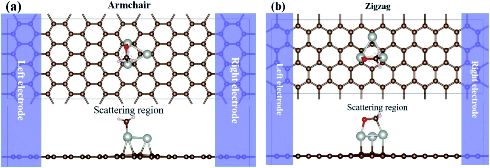
The HCHO sensing properties of the Pdn/graphene systems are carried out by the NEGF-DFT method.47,48 Because of the anisotropy of graphene lattice, the nano-sensor devices are modeled for two different transport directions, i.e. the armchair- and zigzag-directions. The two-probe devices are consisted of the left/right electrode, the central scattering region that is made up with the Pdn cluster supported on the graphene with/without HCHO adsorption. For the Pdn clusters on graphene without and with HCHO gas adsorption the optimized atomic structures are presented in Fig. 2 and 4, and these stable structures do not need to optimize again since they are independent of the transport directions. The sensor models, using HCHO adsorption on Pd3/graphene as the example, are illustrated in Fig. 7. The atomic structures of the central scattering region are fully relaxed as discussed above.
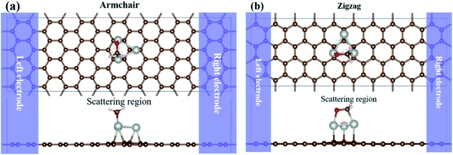 |
| | Fig. 7 Two-probe nano-sensor device models, using HCHO adsorption on Pd3/graphene as the example. The semi-infinite left and right graphene electrodes (shaded zones) are in contact with the scattering region. Both the top and side views of the devices along the armchair (a) and zigzag (b) directions are shown. The C, Pd, O and H atoms are shown in brown, silver, red and white balls, respectively. | |
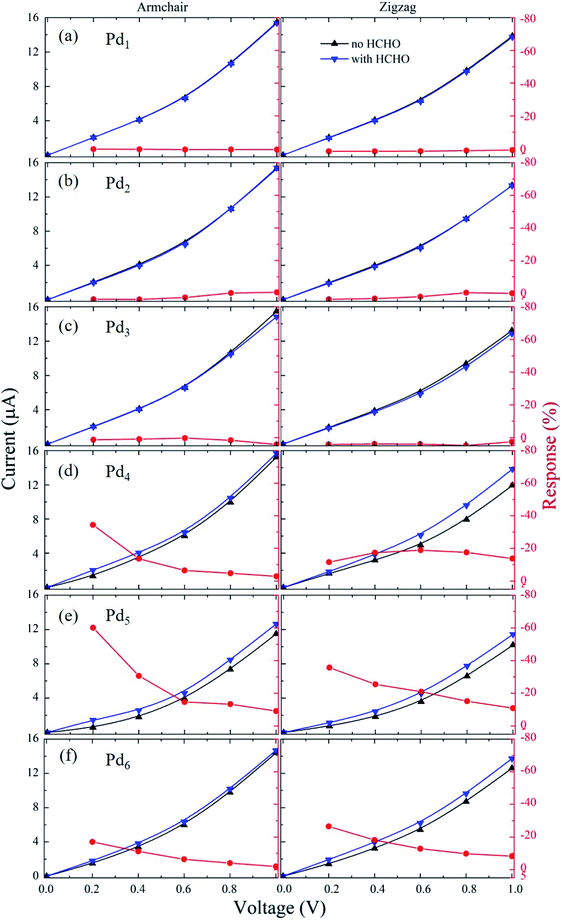
The sensing performance can be evaluated in terms of the sensor response (S),49,50 which is defined as the resistance difference after gas adsorption and before gas adsorption divided by the resistance without gas adsorption. According to this definition, we have S = [(Rg − R0)/R0] × 100% = [(I0 − Ig)/Ig] × 100%, in which the initial electronic resistance/current of the sensor without HCHO adsorption is R0/I0 and the resistance/current with HCHO adsorption is Rg/Ig. We have simulated the current–voltage (I–V) curves of all the Pdn/graphene cases with and without HCHO adsorption under the bias voltage from 0 to 1 V. The I–V and response results are presented in Fig. 8. The current increases as increasing the applied voltage for all the nano-sensors along both the armchair and zigzag transport directions. For the HCHO molecule adsorption on Pdn/graphene (n = 1–3), it is found that the currents passing through the nano-devices are almost same before and after HCHO adsorption in the whole applied voltage range. So the responses for these nano-sensors are insensitive regarding the HCHO gas adsorption. As shown in Fig. 8(d–f) for the large Pdn (n ≥ 4) cluster cases, the electronic current of the sensor with HCHO adsorption starts to differ from that without HCHO adsorption. The current is increased upon the HCHO adsorption relative to the case without HCHO adsorption. The corresponding responses are also substantially larger than those for the Pdn (n = 1–3) cluster systems. We can see that the sensor response depends on the applied voltage and generally decreases as the applied voltage increases. The dependence of response on the applied voltage will be discussed below. A large response at the small bias voltage implies that the device has a short response time and a high sensitivity. Therefore, these devices with the highest absolute response over 20% at small bias voltages should be sensitive enough for the HCHO gas detecting.51–53 Especially, for the armchair-orientated Pd5/graphene nano-sensor it has the highest absolute response over 60% at 0.2 V, indicating its suitability of HCHO sensing.
 |
| | Fig. 8 The current–voltage curves and responses of the armchair- and zigzag-orientated nano-sensor devices constructed from Pdn/graphene (n = 1–6) under the bias voltage from 0 to 1.0 V are presented in (a–f). | |
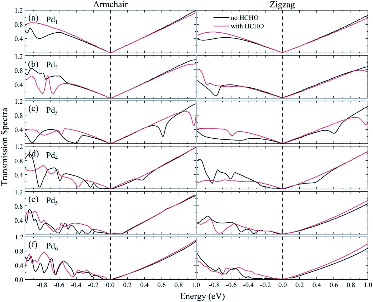
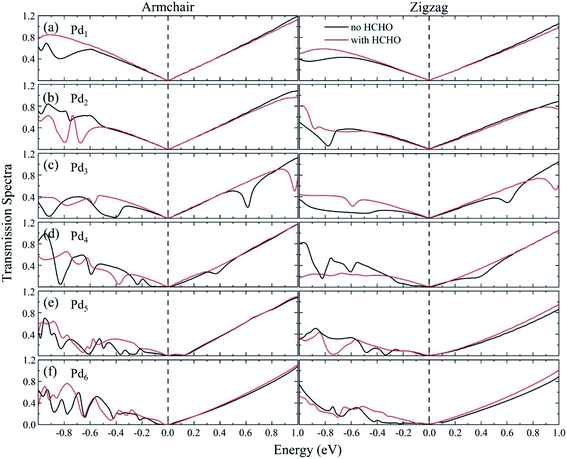
The transmission spectra in the equilibrium situation with zero bias for the Pdn/graphene substrate adsorbed with/without HCHO molecule are plotted in Fig. 9. The transmission spectra exhibit a dependence on the size and geometry of the Pdn cluster. For the Pdn (n = 1–3) cases, the transmission spectra near zero bias are relatively smoother compared to those for the larger Pdn (n = 4–6) clusters and almost same before and after HCHO adsorption. This explains why the nano devices consisted of the Pdn (n = 1–3) clusters are insensitive with respect to the HCHO adsorption for these cases. For the larger Pdn (n = 4–6) cases we see that the transmission spectra are quite different on the left side of zero bias before and after HCHO adsorption. The transmission spectra vary irregularly without HCHO adsorption, which is mainly attributed to the electron scattering effect of the complex local deformation of graphene loaded with a larger Pdn cluster. Upon the HCHO adsorption, the interaction between the Pdn cluster and graphene is weakened caused by the interaction between the HCHO and the Pdn cluster supported on graphene, and consequently the electron scattering effect of graphene local deformation becomes relatively weaker compared to the case without HCHO adsorption. From Table 2 we can see that for the Pdn (n = 3–6) cases the graphene electron gains before and after HCHO adsorption have a very small change. The electron gain of graphene for the Pd3 case is similar to those for other Pdn (n = 4–6) cases, but the current increases are quite different for all the four cases. This indicates that the current change after HCHO adsorption can be mainly attributed to the graphene scattering effect, rather than the number change of charge carriers. The transmission coefficients for the HCHO adsorption cases are generally larger than those without HCHO adsorption, which is consistent with the current–voltage results in Fig. 8.
 |
| | Fig. 9 Transmission spectra for the Pdn/graphene (n = 1–6) sensors without and with HCHO adsorption at zero bias are shown in (a–f). The dashed lines, which are set to be zero on the energy scale, indicate the Fermi level. | |
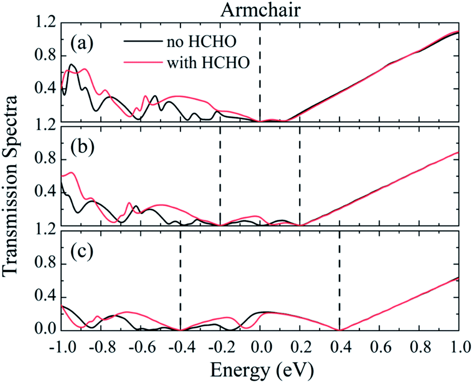
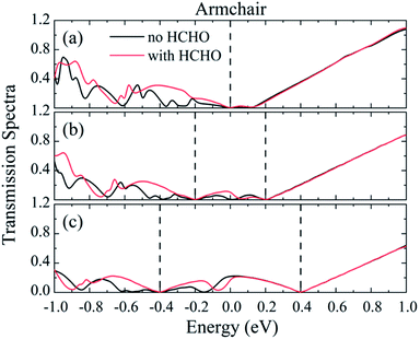
In order to understand the larger response under low bias voltages, the transmission spectra of the nano-sensor constructed from Pd5/graphene along the armchair-direction are presented in Fig. 10. We see that within the voltage window (indicated by the dashed lines) the transmission spectra differ from each other before and after HCHO adsorption. The transmission spectrum change before and after HCHO adsorption results in the response of HCHO adsorption, and the integration of the transmission spectrum within the voltage window determines the current. According to the definition of response, it is the ratio of the current difference before and after gas adsorption to the current without gas adsorption. Since the current is low under low bias voltage the response of nano-sensor under low bias voltages can be larger than those under high bias voltages.
 |
| | Fig. 10 The transmission spectra of HCHO nano-sensor constructed from Pd5/graphene along the armchair-direction under (a–c) 0, 0.4 and 0.8 V bias. The dashed lines represent the bias windows. | |
4. Conclusions
The HCHO sensing properties of small Pdn (n = 1–6) cluster decorated graphene have been systematically investigated by performing first-principles calculations in the framework of density-functional theory. The optimized geometries of Pdn cluster decorated graphene with and without HCHO adsorption, adsorption energies and charge transfers are obtained and analyzed for various Pdn cluster cases. The adsorption strength of HCHO gas molecule on the Pdn cluster decorated graphene is dependent on the cluster size and can be tuned in a wide range from −0.68 eV on Pd(111) to −1.98 eV on the Pd3 cluster decorated graphene. The calculated results show that the Pdn (n = 5 and 6) cluster decorated graphene systems have a proper adsorption energy for the HCHO sensing. The adsorbed HCHO gas molecule gains electrons from the Pdn cluster decorated graphene, acting as an acceptor. The HCHO adsorption strength is found to be correlated with the electron gain and C–O bond length. The two-probe sensor devices consisting of the central scattering region and pristine graphene electrodes with the armchair and zigzag transport directions are built, and the current–voltage curves are calculated by the non-equilibrium Green's function method. The results indicate that the devices constructed from the large Pdn (n ≥ 4) cluster decorated graphene are sensitive enough for HCHO detecting with the highest absolute response value over 20% at small bias voltages. Combined with the adsorption energy results we consider that the devices constructed from the Pdn (n = 5 and 6) cluster decorated graphene should be suitable for HCHO gas sensing. The present work provides a useful guidance for designing the HCHO gas sensors based on small metal cluster decorated graphene.
Conflicts of interest
The authors declare no academic misconducts or competing financial interest.
Acknowledgements
The present study was supported by the National Natural Science Foundation of China (Grant No. 11704041) and GRINM Innovation Foundation fund project.
References
- K. Kawamura, K. Kerman, M. Fujihara, N. Nagatani, T. Hashiba and E. Tamiya, Sens. Actuators, B, 2005, 105, 495–501 CrossRef CAS.
- T. Salthammer, S. Mentese and R. Marutzky, Chem. Rev., 2010, 110, 2536–2572 CrossRef CAS PubMed.
- R. D. Timothy, N. R. Carey, P. Susan, C. D. Glass, B. Geza, R. Alison and F. Lin, Ann. Occup. Hyg., 2015, 60, 132–138 Search PubMed.
- S. Suresh and T. J. Bandosz, Carbon, 2018, 137, 207–221 CrossRef CAS.
- J. K. McLaughlin, Int. Arch. Occup. Environ. Health, 1994, 66, 295–301 CrossRef CAS PubMed.
- A. Duong, C. Steinmaus, C. M. McHale, C. P. Vaughan and L. Zhang, Mutat. Res., Rev. Mutat. Res., 2011, 728, 118–138 CrossRef CAS PubMed.
- Q. Huang, D. Zeng, H. Li and C. Xie, Nanoscale, 2012, 4, 5651–5658 RSC.
- P. R. Chung, C. T. Tzeng, M. T. Ke and C. Y. Lee, Sensors, 2013, 13, 4468–4484 CrossRef CAS PubMed.
- D. Chen and Y. J. Yuan, IEEE Sens. J., 2015, 15, 6749–6760 CAS.
- I. Cabria, M. J. López, S. Fraile and J. A. Alonso, J. Phys. Chem. C, 2012, 116, 21179–21189 CrossRef CAS.
- R. Hussain, M. Saeed, M. Y. Mehboob, S. U. Khan, M. Usman Khan, M. Adnan, M. Ahmed, J. Iqbal and K. Ayub, RSC Adv., 2020, 10, 20595–20607 RSC.
- A. Safavi, N. Maleki, F. Farjami and E. Farjami, J. Electroanal. Chem., 2009, 626, 75–79 CrossRef CAS.
- F. Niu and Q. Yi, Rare Met., 2011, 30, 102–105 CrossRef CAS.
- H. Yin, H. Tang, D. Wang, Y. Gao and Z. Tang, ACS Nano., 2012, 6, 8288–8297 CrossRef CAS PubMed.
- D. Sen, R. Thapa and K. K. Chattopadhyay, Int. J. Hydrog. Energy, 2013, 38, 3041–3049 CrossRef CAS.
- A. Gutés, B. Hsia, A. Sussman, W. Mickelson, A. Zettl, C. Carraro and R. Maboudian, Nanoscale, 2012, 4, 438–440 RSC.
- W. Dong, Y. Ren, Z. Bai, Y. Yang and Q. Chen, Bioelectrochem, 2019, 128, 274–282 CrossRef CAS PubMed.
- R. Kumar, D. Varandani, B. R. Mehta, V. N. Singh, Z. Wen, X. Feng and K. Mullen, Nanotechnology, 2011, 22, 275719 CrossRef PubMed.
- Y. Y. Fan, H. L. Tu, Y. Pang, F. Wei, H. B. Zhao, Y. Yang and T. L. Ren, Rare Met., 2020, 39, 651–658 CrossRef CAS.
- Q. Yi, F. Niu and W. Yu, Thin Solid Films, 2011, 519, 3155–3161 CrossRef CAS.
- K. Czelej, K. Cwieka, J. C. Colmenares and K. J. Kurzydlowski, Langmuir, 2016, 32, 7493–7502 CrossRef CAS PubMed.
- M. Yoosefian, H. Raissi and A. Mola, Sens. Actuators, B, 2015, 212, 55–62 CrossRef CAS.
- J. Deng, W. Song, M. Jing, T. Yu, Z. Zhao, C. Xu and J. Liu, Catal. Today, 2020, 339, 210–219 CrossRef CAS.
- L. Yang, W. Xiao, J. Wang, X. Li and L. Wang, J. Mater. Sci., 2021, 56, 12256–12269 CrossRef CAS.
- G. Kresse and J. Furthmüller, Comput. Mater. Sci., 1996, 6, 15–50 CrossRef CAS.
- G. Kresse and J. Furthmüller, Phys. Rev. B: Condens. Matter Mater. Phys., 1996, 54, 11169 CrossRef CAS PubMed.
- J. P. Perdew, K. Burke and M. Ernzerhof, Phys. Rev. Lett., 1996, 77, 3865 CrossRef CAS PubMed.
- G. Kresse and D. Joubert, Phys. Rev. B: Condens. Matter Mater. Phys., 1999, 59, 1758–1775 CrossRef CAS.
- S. Grimme, J. Comput. Chem., 2006, 27, 1787–1799 CrossRef CAS PubMed.
- J. Zhou, Q. Wang, Q. Sun, X. Chen, Y. Kawazoe and P. Jena, Nano Lett., 2009, 9, 3867–3870 CrossRef CAS PubMed.
- G. Henkelman, A. Arnaldsson and H. Jónsson, Comput. Mater. Sci., 2006, 36, 354–360 CrossRef.
- W. Tang, E. Sanville and G. Henkelman, J. Phys.: Condens. Matter, 2009, 21, 084204 CrossRef CAS PubMed.
- J. Taylor, H. Guo and J. Wang, Phys. Rev. B: Condens. Matter Mater. Phys., 2001, 63, 245407 CrossRef.
- D. Waldron, P. Haney, B. Larade, A. MacDonald and H. Guo, Phys. Rev. Lett., 2006, 96, 166804 CrossRef PubMed.
- M. Brandbyge, N. Kobayashi and M. Tsukada, Phys. Rev. B: Condens. Matter Mater. Phys., 1999, 60, 17064–17070 CrossRef CAS.
- M. Brandbyge, J. L. Mozos, P. Ordejón, J. Taylor and K. Stokbro, Phys. Rev. B: Condens. Matter Mater. Phys., 2002, 65, 165401 CrossRef.
- S. Datta, Quantum transport: atom to transistor, Cambridge University Press, 2005 Search PubMed.
- M. Büttiker, Y. Imry, R. Landauer and S. Pinhas, Phys. Rev. B: Condens. Matter Mater. Phys., 1985, 31, 6207–6215 CrossRef PubMed.
- J. Rogan, G. García, J. A. Valdivia, W. Orellana, A. H. Romero, R. Ramírez and M. Kiwi, Phys. Rev. B: Condens. Matter Mater. Phys., 2005, 72, 115421 CrossRef.
- J. A. Alonso, Structure and properties of atomic nanoclusters, Imperial College Press, London, 2005 Search PubMed.
- I. Cabria, M. J. López and J. A. Alonso, Phys. Rev. B: Condens. Matter Mater. Phys., 2010, 81, 035403 CrossRef.
- W. Xiao, R. Zeng, L. Cheng, J. W. Wang, L. J. Jiang and L. G. Wang, RSC Adv., 2015, 5, 61861–61867 RSC.
- E. Jeroro and J. M. Vohs, J. Am. Chem. Soc., 2008, 130, 10199–10207 CrossRef CAS PubMed.
- X. K. Gu and W. X. Li, J. Phys. Chem. C, 2010, 114, 21539–21547 CrossRef CAS.
- X. Chen, L. Xu, L. L. Liu, L. S. Zhao, C. P. Chen, Y. Zhang and X. C. Wang, Appl. Surf. Sci., 2017, 396, 1020–1025 CrossRef CAS.
- M. Zhou, Y. H. Lu, Y. Q. Cai, C. Zhang and Y. P. Feng, Nanotechnology, 2011, 22, 385502 CrossRef PubMed.
- D. B. Farmer, R. Golizadeh Mojarad, V. Perebeinos, Y. M. Lin, G. S. Tulevski, J. C. Tsang and P. Avouris, Nano Lett., 2009, 9, 388–392 CrossRef CAS PubMed.
- L. Kou, T. Frauenheim and C. Chen, J. Phys. Chem. Lett., 2014, 5, 2675–2681 CrossRef CAS PubMed.
- K. Lee, R. Gatensby, N. McEvoy, T. Hallam and G. S. Duesberg, Adv. Mater., 2013, 25, 6699–6702 CrossRef CAS PubMed.
- S. Yang, C. Jiang and S. h. Wei, Appl. Phys. Rev., 2017, 4, 021304 Search PubMed.
- A. J. Yang, D. W. Wang, X. H. Wang, J. F. Chu, P. L. Lv, Y. Liu and M. Z. Rong, IEEE Electron Device Lett., 2017, 38, 963–966 CAS.
- S. J. Young and Z. D. Lin, ECS J. Solid State Sci. Technol., 2017, 6, M130–M132 CrossRef CAS.
- F. Niu, L. M. Tao, Y. C. Deng, Q. H. Wang and W. G. Song, New J. Chem., 2014, 38, 2269–2272 RSC.
Footnote |
| † Electronic supplementary information (ESI) available. See DOI: 10.1039/d1ra06940c |
|
| This journal is © The Royal Society of Chemistry 2021 |
Click here to see how this site uses Cookies. View our privacy policy here. 
 Open Access Article
 This Open Access Article is licensed under a Creative Commons Attribution-Non Commercial 3.0 Unported Licence
 abcd,
Wei Xiaoabc,
Jianwei Wangabc,
Xiaowu Lid and
Ligen Wang*abc
abcd,
Wei Xiaoabc,
Jianwei Wangabc,
Xiaowu Lid and
Ligen Wang*abc
 is the unit of the quantum conductance and f(E − μL/R) is the Fermi–Dirac distribution function of the left/right electrode.