DOI:
10.1039/D1RA06807E
(Paper)
RSC Adv., 2021,
11, 37559-37567
Near-infrared tunable surface plasmon resonance sensors based on graphene plasmons via electrostatic gating control
Received
10th September 2021
, Accepted 16th November 2021
First published on 22nd November 2021
Abstract
A tunable near-infrared surface plasmon resonance sensor based on graphene plasmons via electrostatic gating control is investigated theoretically. Instead of the traditional refractive index sensing, the sensor can respond sensitively to the change of the chemical potential in graphene caused by the attachment of the analyte molecules. This feature can be potentially used for biological sensing with high sensitivity and high specificity. Theoretical calculations show that the chemical potential sensing sensitivities under wavelength interrogation patterns are 1.5, 2.21, 3, 3.79, 4.64 nm meV−1 at different wavebands with centre wavelengths of 1100, 1310, 1550, 1700, 1900 nm respectively, and the full width half maximum (FWHM) is also evaluated to be 10, 25.5, 43, 55.5, 77 nm at these different wavebands respectively. It can be estimated that the theoretical limit of detection (LOD) in DNA sensing of the proposed sensor can reach the femtomolar level, several orders of magnitude superior to that of noble metal-based SPR sensors (nanomolar or subnanomolar scale), and is comparable to that of noble metal-based SPR sensors with graphene/Au-NPs as a sensitivity enhancement strategy. The FWHM is much smaller than that of the noble metal-based SPR sensors, making the proposed sensor have a potentially higher figure of merit (FOM). This work provides a new way of thinking to detect in an SPR manner the analyte that can cause chemical potential change in graphene and provides a beneficial complement to refractive index sensing SPR sensors.
1. Introduction
Surface plasmon resonance (SPR) is a powerful optical sensing technology which relies on plasmons, the collective density oscillations of an electron liquid that exist in many metals and semiconductors. In a conventional SPR sensing scheme, a thin metal film (Au, Ag, Cu, Al, etc.) is deposited on a prism base and p-polarized incident light excites the surface plasmon polariton at the metal/dielectric (analytes) interface. Due to the highly sensitive, label free, and real time sensing of the change of the refractive index of the analyte, SPR sensors are widely used in chemical and biological sensing. While there exist some limiting factors that hinder further applications of SPR sensors: (1) the nature of refractive index sensing of the SPR sensors makes them have poor specificity.1 (2) When the change of the analyte concentration may not cause significant refractive index variations (for instance of gas sensing), SPR sensors display poor sensitivity. (3) The working wavelengths of noble metal-based SPR sensors are limited to visible spectrum and near-infrared spectrum that very closed to visible waveband, and generally cannot be tuned.
Thanks for discovery of graphene, a two-dimensional sheet of carbon atoms arranged in honeycomb lattice, the limiting factors of SPR sensors mentioned above are expected to be overcome. Combining graphene with metal film to make graphene enhanced metal SPR (GEMSPR) sensors has attracted many attentions. Graphene-on-gold structure was firstly considered and the sensitivity enhancing was demonstrated theoretically.2 To further enhance the sensitivity, some more complex heterostructures such as graphene–Si–metal,3 graphene–MoS2–metal,4–6 graphene–WS2–metal,7 graphene–black phosphorus–metal,8 WSe2–WS2–MoS2–graphene–metal,9 etc., were also considered. Graphene-on-gold SPR imaging platform with a ca. 40% sensitivity enhancement was demonstrated experimentally10 and highly sensitive GEMSPR sensors were used for biological sensing,11–15 even gas sensing.16,17 Although GEMSPR sensors can greatly enhance the performance in term of sensitivity comparing with the conventional SPR sensors, their intrinsic refractive index sensing character are still reserved. Furthermore, the working wavelengths of GEMSPR sensors are also limited to visible spectrum and near-IR spectrum that very closed to visible waveband and are still nonadjustable.
As a two-dimensional semiconductor, graphene can also support plasmons that different from those in noble metals as they can be tuned by gating or doping.18,19 The optical studies of graphene plasmon in the early stage were mostly motivated by terahertz plasmon studies in traditional 2D electron gas system.20 Therefore, the study of graphene plasmon mainly focuses on the terahertz to mid-IR waveband, such as localized plasmons in graphene nanostructures,21–23 propagating plasmons excited by metallic tip,24 etc. Attempts have also been made to extend the study of graphene plasmon to near-IR and even visible waveband.25,26 The unique and intriguing fundamental properties, such as enabling strong confinement of electromagnetic energy at sub-wavelength scales,27 tunable and controllable via electric field,28 magnetic field,29,30 and light field,31 existing new polarization mode,32,33 etc., provide an advantage for graphene plasmon over surface plasmon on a metal–dielectric interface. Graphene can be used instead of metal film to manufacture graphene SPR (GSPR) sensors. Despite the theoretically predicted tunability, a key challenge of GSPR sensors is to overcome the momentum mismatch between the free-space waves and the plasmon modes in graphene. Spatial-beam configuration tunable mid-IR graphene plasmonic sensors have been realized for protein detection34 and gas identification35 by using light beam incident directly on graphene nanoribbon arrays (GNA). A prism configuration GNA-based mid-IR GSPR sensor was also demonstrated theoretically which relies on the graphene chemical potential scan for refractive index sensing.36 These all benefit from the plasmon resonances bounded in graphene nanoribbons which can be tuned by changing the ribbon width and the doping level of graphene.21 In addition to GNA, a silicon diffractive grating underneath a graphene sheet can also be used to excite mid-IR plasmon mode in graphene through guided-wave resonance caused by a normal-incidence light beam.37 In terahertz spectrum, it was found that the momentum mismatch between the highly confined plasmon modes in homogeneous graphene sheets and the incident radiation could be alleviated by increasing the surface conductivity of graphene through high doping levels or with few layer graphene, and by adopting high-index coupling prism.38 Several prism configuration GSPR sensors with doped graphene for angular interrogation sensing,39 frequency interrogation sensing,40 and phase interrogation sensing41 in THz spectrum were studied theoretically.
In this paper a design of prism configuration GSPR sensor that can work in near-IR spectrum via electrostatic gating control is put forward, and the sensing performance is investigated theoretically. The momentum mismatch between the plasmon modes in homogeneous graphene sheets and the incident near-IR radiation could be alleviated by adjusting the chemical potential to be close to the epsilon-near-zero (ENZ) point. By using Si3N4 as a dielectric layer, which has a large relative permittivity and a large breakdown field, the chemical potential of graphene can be adjusted to be close to the ENZ point in near-IR spectrum through electrostatic gating without the breakdown. Based on this, the SPR sensing technology is expected to be realized in the near-IR spectrum which is slightly farther from the visible spectrum, especially in the wavelength range of 1310–2000 nm of existing mature light sources and light detection instruments. The chemical potential sensing (instead of refractive index sensing) feature make the proposed near-IR tunable GSPR sensor has great potential to be used in highly sensitive and high specificity biological and chemical sensing.
2. Structure design and physical mechanism
The proposed sensor takes Otto prism coupling structure as shown in Fig. 1. A 50 nm thick Si3N4 layer sandwiched between two graphene sheets (both 5-atom-layer) is placed on a substrate of MgF2. A prism is placed on the upside of the top graphene sheet with a gap between them for filling with analyte. A p-polarized laser beam incidents from a side of prism with an incident angle of θ, reflected by the bottom side, then emit through the another side of prism. By adding a gate voltage between the two graphene sheets, they can gate each other42 for adjusting their own chemical potentials (absolute value) to a proper value at which the SPR effect of graphene would happen. When the top graphene sheet is attached by analyte molecules, charge transfer (or electrostatic gating) between it and the analyte molecules would cause the chemical potential of it changing further, this would shift the resonance wavelength or resonance angle.
 |
| | Fig. 1 Schematic diagram of the sensor. | |
Since the chemically vapor deposited (CVD) mono-atom layer graphene with up to wafer size is already commercially available, it is realistic and feasible to fabricate the structure like in Fig. 1. Using and repeating the standard wet transfer method,43 the randomly stacked few-atom layer bottom graphene sheet can be placed on the MgF2 substrate. The Si3N4 dielectric layer can be deposited on the bottom graphene sheet by using plasma-enhanced chemical vapor deposition (PECVD) method.44 The few-atom layer top graphene sheet can be prepared by using the same procedure as that used for the bottom graphene sheet. The Au electrodes attached to graphene sheets (top and bottom) can be prepared by using e-beam evaporation method. The sensor structure can also be designed to adopt the Kretschmann configuration and it is found through calculation that the sensing performance are similar to that of Otto configuration one. The relevant research is described in our another paper in preparation.
The dynamic conductivity of graphene can be obtained from Kubo formula:45
| |
 | (1) |
where
ω,
μc,
Γ,
T, j,
e,
ε and
ħ are radian frequency, chemical potential, scattering rate, temperature, imaginary unit, electron charge, energy and reduced Planks constant respectively.
fd(
ε) = {1 + exp[(
ε −
μc)/
kBT]}
−1 is the Fermi–Dirac distribution,
kB is Boltzmann's constant. The relative permittivity
εg and the refractive index
ng of graphene is related to its dynamic conductivity by:
46| |
 | (2) |
where
ε0 and
tg = 0.34 nm are the permittivity of free space and thickness of graphene respectively. By using
eqn (1) and
(2) we can calculate the dielectric constant as a function of both the chemical potential and frequency of light under the condition of
T = 298 K and
Γ = 1 × 10
12 Hz, as shown in
Fig. 2. The demarcation chemical potential
μc0 for graphene changing from dielectric to metallic is called ENZ point at which the absolute value of relative permittivity of graphene is near zero. It is interesting that the ENZ point possesses almost linear dependence on the frequency of light within near-IR spectrum,
i.e. μc0(
ω) ≈ 0.63
ħω, as shown in
Fig. 2(b). So with the increase of frequency (decrease of wavelength),
μc0 would become larger, as shown in
Fig. 2(c).
 |
| | Fig. 2 (a) Relative permittivity of graphene as a function of its chemical potential under the conditions of λ = 1310 nm, T = 298 K, Γ = 1 × 10¹² Hz; (b) the absolute value of relative permittivity with both wavelength and chemical potential in unit of hω/2π; (c) the absolute value of relative permittivity with both wavelength and chemical potential in unit of eV. | |
To excite the surface plasmon resonance in graphene sheet, the p-polarized incident light should match both the wave vector and energy of the surface plasmon in graphene sheet.
Generally speaking the wave vector of surface plasmon wave in graphene sheet is much larger than that of incident light.33 While at ENZ point, the absolute value of refractive index of graphene reaches its minimum (near zero), the wave vector of the surface plasmon wave in graphene sheet can be greatly reduced. So the required chemical potential for arousing SPR effect in graphene sheet (called plasmon resonance point, or PR point, marked as μcPR) must be near the ENZ point and can be calculated through finite element mode analysis in COMSOL (see part 4 of this paper). The ENZ points as well as the PR points at different wavelengths are listed in Table 1. It can be found that the smaller the resonance wavelength λ, the larger the μcPR(λ) will be. It is also obvious that within near-IR spectrum the PR points are all larger than 0.3 eV (for naturally doped graphene, μc ≲ 0.3 eV (ref. 46)), which means that generally speaking the SPR effect of naturally doped graphene cannot be aroused by near-IR incident light (let alone by visible incident light). By adding gate voltage, the chemical potential of graphene can be adjusted to PR point for arousing SPR effect of graphene by incident light within near-IR spectrum. The corresponding required gate voltages can be calculated by using:47
| | |
C(VDC − VDirac) = ens
| (3) |
and
45| |
 | (4) |
where
VDirac is the voltage at the Dirac point,
VDC is applied DC bias field,
C =
ε0εr/
t is the gate capacitance (on unit graphene area),
εr and
t are relative permittivity and thickness of Si
3N
4 layer respectively, and
vF ≈ 9.5 × 10
5 m s
−1 is the Fermi velocity. For undoped graphene,
VDirac = 0, the required gate voltages (at wavelengths of 760, 850, 980, 1100, 1310, 1550, 1700, and 1900 nm respectively) can be calculated and listed in
Table 1 too. The breakdown field of Si
3N
4 is about 11.5 MV cm
−1,
44 i.e. the breakdown voltage of 50 nm-thick Si
3N
4 is about 57.5 V. So the sensor can work in the waveband of
λ ≥ 1100 nm.
Table 1 ENZ points, PR points, required gate voltages for arousing SPR effect of graphene at different wavelengths
| λ (nm) |
760 |
850 |
980 |
1100 |
| μc0 (eV) |
1.037 |
0.923 |
0.798 |
0.709 |
| μcPR (eV) |
1.048 |
0.930 |
0.802 |
0.712 |
| Vg (V) |
122 |
96 |
72 |
57 |
| λ (nm) |
1310 |
1550 |
1700 |
1900 |
| μc0 (eV) |
0.594 |
0.502 |
0.458 |
0.410 |
| μcPR (eV) |
0.596 |
0.503 |
0.459 |
0.411 |
| Vg (V) |
40 |
28 |
24 |
19 |
3. Numerical method and optimal consideration
The transfer matrix method (TMM) for N-layer model is applied for the calculation of reflectivity of the reflective light. The refractive index and the thickness of the kth layer are considered as nk and dk respectively. For p-polarized light, the characteristic matrix of the combined structure of sensor can be given as:4| |
 | (5) |
with| |
 | (6) |
where| |
 | (7) |
and| |
 | (8) |
where λ is the wavelength of the incident light. The reflection coefficient for p-polarized light is given as:| |
 | (9) |
The reflectance of the defined multilayer configuration is:
Several representative materials were considered to form prism: CaF2 (1.4261), ZBLAN (1.4688), BK7 (1.515), SF11 (1.7786), 2S2G (2.241), Si (3.47). In order to choose an optimal material of prism, angular interrogation method is employed to inspect the SPR curves by using a monochromatic light beam incident. The refractive indices of analyte, Si3N4, and MgF2 can be taken as 1.33, 2.57, and 1.37 respectively. The chemical potentials of the top and the bottom graphene sheets are adjusted to the PR points. The thicknesses of graphene sheets and Si3N4 are 5 × 0.34 nm, and 50 nm respectively. The thickness of analyte layer is temporarily set at 1 nm. The reflectance versus incident angle curve of monochromatic light beams (with wavelength of 1100, 1310, 1550, 1900 nm respectively) for different materials of the prism are calculated and depicted in Fig. 3. The first minimum reflectance point on the curve from the right-hand side indicates the occurrence of the SPR effect of the graphene. The vertical coordinate of this point can be marked as Rmin, and the horizontal coordinate of this point corresponds to resonance angle. For the case of 1100 nm, with the increase of the refractive index of the prism material, Rmin decrease gradually and reaches its minimum at Si (3.47), as shown in Fig. 3(a). For the case of 1310 nm, with the increase of the refractive index of the prism material, Rmin firstly decrease gradually and reaches its minimum at BK7 (1.515), and then increase gradually, as shown in Fig. 3(b). For the cases of 1550 nm and 1900 nm, Rmin all reaches its minimum at CaF2 (1.4261), as shown in Fig. 3(c) and (d). It can be seen that with the increase of the wavelength of the incident light, the refractive index of the optimal material of the prism becomes smaller.
 |
| | Fig. 3 Reflectance versus incident angle curves for different prism materials when using incident monochromatic light beam with different wavelength: (a) 1100 nm; (b) 1310 nm; (c) 1550 nm; (d) 1900 nm. | |
The optimal thickness of the analyte layer ta is then investigated through angular interrogation method. For the different wavelength of 1100, 1310, 1550, 1700, and 1900 nm, by adopting the optimal materials of prism for each wavelength, i.e. Si for 1100 nm, BK7 for 1310 nm, CaF2 for 1550, 1700, and 1900 nm respectively, the SPR curves at different ta can be calculated and the last four are depicted in Fig. 4(a)–(d) respectively. Accordingly, the Rmin versus ta curves for the different wavelength of 1310, 1550, 1700, and 1900 nm are depicted in Fig. 5(a)–(d) respectively. So considering not only Rmin, but also the actual size of the analyte molecules (such as biomolecules), we take the optimal thickness of the analyte layer to be 300 nm. The resonance angle also changes with ta. When ta = 300 nm, the resonance angle can be obtained as 24.1°, 65.4°, 74.2°, 74.1°, and 74° for different wavelength of 1100, 1310, 1550, 1700, and 1900 nm respectively.
 |
| | Fig. 4 Reflectance versus incident angle curves for different thickness of the analyte layer when using incident monochromatic light beam with different wavelength: (a) 1310 nm; (b) 1550 nm; (c) 1700 nm; (d) 1900 nm. | |
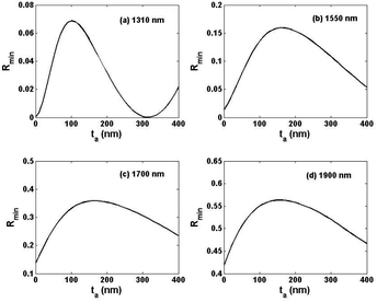 |
| | Fig. 5 Rmin as a function of ta for different wavelength of incident light beam: (a) 1310 nm; (b) 1550 nm; (c) 1700 nm; (d) 1900 nm. | |
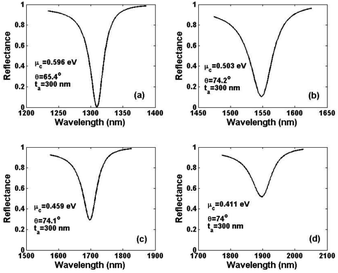
In order to inspect the sensing characteristics of the sensor under wavelength interrogation pattern, the chemical potentials of the top and the bottom graphene sheets were all adjusted to the PR point μcPR(λ′), and a broadband light beam with λ′ as a central wavelength was incident. The refractive index of graphene ng(λ) as a function of λ (around λ′) can be calculated through eqn (1) and (2) under the conditions of μc = μcPR(λ′), T = 298 K, Γ = 1 × 10¹² Hz. The reflectance curves at different wavebands with central wavelengths of 1100, 1310, 1550, 1700, and 1900 nm respectively are calculated and the last four are depicted in Fig. 6. In calculation the thickness of the analyte layer were taken as ta = 300 nm; the optimal materials of prism are adopted for each central wavelength, i.e. Si for 1100 nm, BK7 for 1310 nm, CaF2 for 1550, 1700, and 1900 nm, respectively. The resonance angles obtained from angular interrogation calculation are adopted for the incident angles, i.e. 24.1°, 65.4°, 74.2°, 74.1°, and 74° for the broadband light beam with central wavelengths of 1100, 1310, 1550, 1700, and 1900 nm, respectively. It can be seen that the FWHM becomes larger with the increase of the resonance wavelength, and they are 10, 25.5, 43, 55.5, and 77 nm for central wavelengths 1100, 1310, 1550, 1700, and 1900 nm respectively. Contrastingly, a graphene oxide–Au GEMSPR sensor with resonance wavelength located in the range of 600–900 nm has a FWHM larger than 100 nm.13 Generally, the FWHM will increase with the resonance wavelength. So it can be inferred that the FWHMs of the proposed near-IR GSPR sensor are much smaller than that of GEMSPR sensors assuming their resonance wavelengths can reach the same near-IR wavelengths (i.e. 1100–2000 nm).
 |
| | Fig. 6 Reflectance versus wavelength curves for the chemical potential of graphene reach the PR point of different wavelength: (a) μc = μcPR (1310 nm); (b) μc = μcPR (1550 nm); (c) μc = μcPR (1700 nm); (d) μc = μcPR (1900 nm). | |
4. Sensing performance based on wavelength interrogation pattern
By adding gate voltage, the chemical potential of the top and the bottom graphene sheets were set to an PR point μcPR(λ′) (thereby the resonance wavelength would be λ′). When the analyte was injected into the space between the prism and the top graphene sheet, two changes would be brought about: one, the chemical potential of the top graphene sheet would be changed further (from the PR point) due to the charge transfer between graphene and the attached analyte molecules; two, the refractive index of the analyte layer would be changed. In order to estimate the response sensitivity of the resonance wavelengths to the change of the chemical potential of the top graphene sheet, the chemical potential of the bottom graphene sheet is set to keep at PR point (because no analyte was attached on it), and the chemical potential of the top graphene sheet is set to change around the PR point, meantime the refractive index of the analyte was assumed to be constant and set to 1.33. The variation of SPR curves in different wavebands with central wavelengths of 1100, 1310, 1550, 1700, and 1900 nm respectively with the change of the chemical potential of the top graphene sheet can be calculated and the last four are depicted in Fig. 7. In calculation the thickness of the analyte layer is taken as ta = 300 nm; the optimal materials of prism are adopted for each central wavelength; the incident angles are 24.1°, 65.4°, 74.2°, 74.1°, and 74° for the broadband light beam with central wavelengths of 1100, 1310, 1550, 1700, and 1900 nm, respectively. With the increase of chemical potential of the top graphene sheet (meanwhile the chemical potential of the bottom graphene sheet keeps constant, i.e. PR point), the resonance wavelengths all shift to smaller values (blue shift). The response sensitivities of the resonance wavelengths to the change of the chemical potential of the top graphene sheet (called CP sensitivity) are about 1.5, 2.21, 3, 3.79, 4.64 nm meV−1 at different wavebands with central wavelengths of 1100, 1310, 1550, 1700, and 1900 nm respectively. With the decrease of the resonance wavelength, the CP sensitivity becomes smaller, as shown in Fig. 8(a). Keep in mind that the refractive index of graphene changes with its chemical potential, the response sensitivity of the resonance wavelengths to the change of the refractive index of the top graphene sheet (called RI sensitivity) can also be estimated, as shown in Fig. 8(b).
 |
| | Fig. 7 The variation of SPR curves in different wavebands with central wavelengths of (a) 1310; (b) 1550; (c) 1700; (d) 1900 nm respectively with the change of the chemical potential of the top graphene sheet. | |
 |
| | Fig. 8 (a) CP sensitivity of the sensor at different resonance wavelength; (b) RI sensitivity of the sensor at different resonance wavelength. | |
In order to estimate the RI sensitivities of the resonance wavelengths to the change of refractive index of the analyte, the chemical potentials of the top and the bottom graphene sheets are all set to PR point μc0(λ′), and the refractive index of the analyte is set to change within the range of 1.33–1.43. The variation of SPR curves at different wavebands with central wavelengths of 1100, 1310, 1550, 1700, and 1900 nm respectively with the refractive index of the analyte can be calculated and the last four are depicted in Fig. 9. With the increase of the refractive index of the analyte, the resonance wavelengths all shift to smaller values, as shown in Fig. 9. The absolute value of the RI sensitivity are about 19, 46, 19, 20, 20 nm per RIU at different wavebands with central wavelengths of 1100, 1310, 1550, 1700, and 1900 nm respectively.
 |
| | Fig. 9 The variation of SPR curves in different wavebands with central wavelengths of (a) 1310; (b) 1550; (c) 1700; (d) 1900 nm respectively with the change of the refractive index of the analyte layer. | |
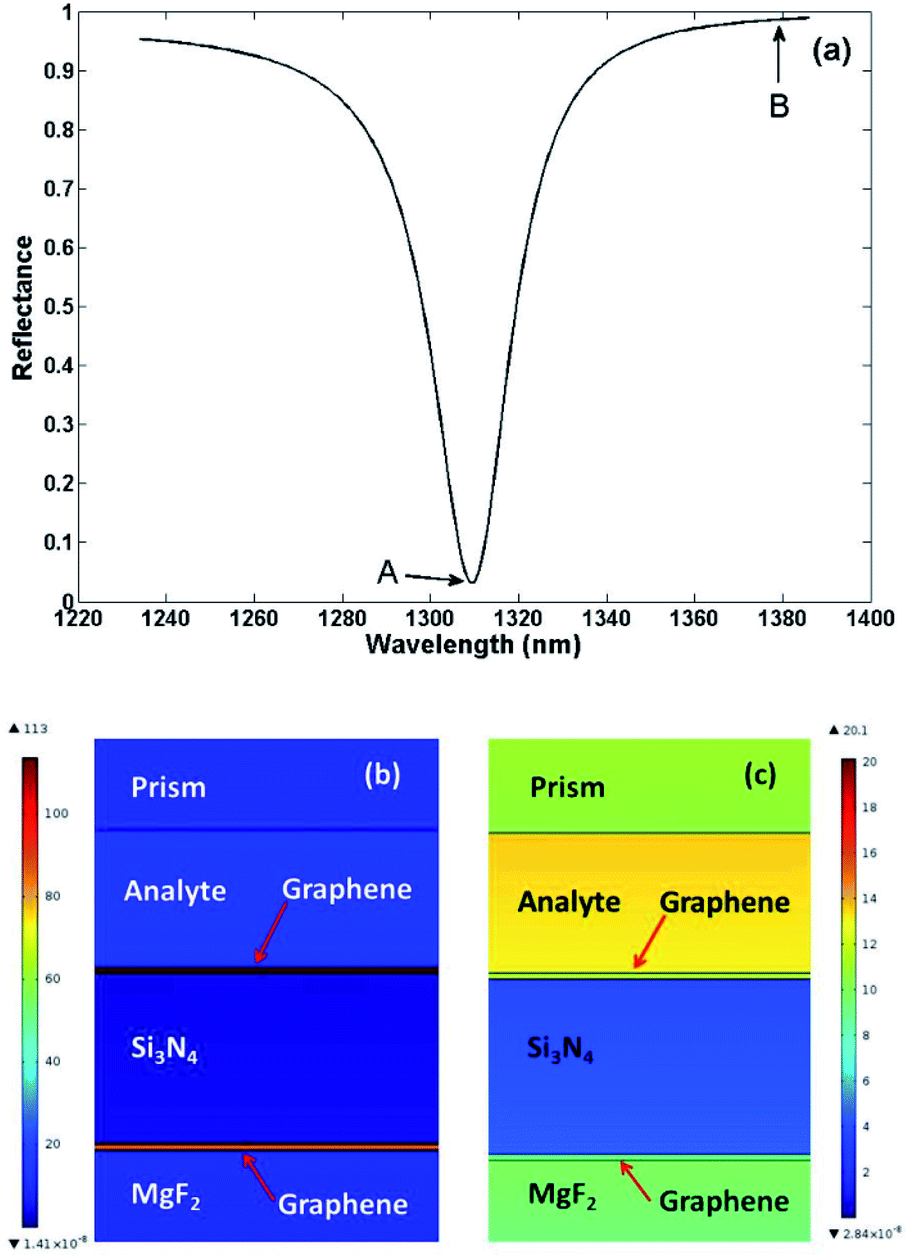
Obviously, the RI sensitivity of the near-IR GSPR sensor to either the change of the refractive index of the top graphene sheet or the change of the refractive index of the analyte is much lower than that of GEMSPR sensors, which typically reach several thousands of nm/RIU,13 even more than 10 thousands of nm per RIU.14 The reason that the resonance wavelength of the near-IR GSPR sensor is insensitive to the change of the refractive index of the analyte is probably because the plasmon is not at the surface of but inside the graphene sheet.48 The 2D finite element method simulation results confirm that the plasmon mode field mainly distributes inside the graphene sheets, as shown in Fig. 10. This is very different from a noble metal-based SPR sensor, in which the plasmon exits at the interface between the metal and the analyte; and this is also different from the GSPR sensors in THz spectrum41 (and even mid-IR spectrum37) in which the plasmon mode has a greater decay length in the direction perpendicular to the graphene plane and penetrates into the analyte. The shift of the resonance wavelength is directly caused by the change of graphene chemical potential, rather than by the change of graphene refractive index, so the near-IR GSPR sensor should be considered to have chemical potential sensing (instead of refractive index sensing) character.
 |
| | Fig. 10 (a) SPR curve in the waveband with 1310 nm as a central wavelength under the condition of ta = 40 nm. The distribution of the electromagnetic field in the cross section of the multi-layer system corresponding to point A and B in (a) are displayed in (b) and (c) respectively. | |
This chemical potential sensing feature can be used for detecting sensitively the analyte whose attachment on graphene can cause a remarkable change of chemical potential in graphene, no matter the refractive index change in the analyte layer caused by the attachment are small (for instance of gas molecules) or large (for instance of bio molecules). It is well known that the attachment of bio molecules on graphene will cause charge transfer (or electrostatic gating) and can change the chemical potential of graphene.49,50 According to Dong et al., the hybridization of 0.01 nM complementary DNAs to the probe DNAs pre-immobilized on graphene would cause >10 meV of chemical potential shift in graphene.50 For a near-IR GSPR sensor proposed in this paper, it would cause >15, >22.1, >30, >37.9, and >46.4 nm of resonance wavelength shifts at different wavebands with central wavelengths of 1100, 1310, 1550, 1700, and 1900 nm respectively. Supposing the wavelength resolution of the optical spectrum analyser (OSA) is 0.02 nm, the proposed near-IR GSPR sensor can reach LOD of <13.33, <9.05, <6.67, <5.28, and <4.31 fM in DNA sensing at different wavebands with central wavelengths of 1100, 1310, 1550, 1700, and 1900 nm respectively. Contrastingly, the LOD of the noble metal-based SPR sensors in DNA sensing are nM or sub-nM scale,51 and the LOD of the GEMSPR sensors with Au-NPs as sensitivity enhancement-strategy in DNA sensing can reach fM or sub-fM scale.52 The selected recent literatures on DNA detection by SPR manner since 2019 are listed in Table 2. Although the LOD has been improved further,54–57 a notable feature is the need to use gold nanoparticles or nanorods as sensitivity enhancement strategy.
Table 2 The selected recent literatures on DNA detection by SPR manner since 2019
| SPR structure |
LOD |
FWHM |
Ref. |
| Fiber/Au film |
80 nM |
— |
53 |
| K9/Au film/GO-AuNPs |
0.2 fM |
— |
54 |
| K9/AuNT array/AuNPs |
1.2 aM |
114.471 nm |
55 |
| K9/Au film/graphene/AuNPs |
0.5 fM |
— |
56 |
| K9/Au film/antimonene/AuNRs |
10 aM |
— |
57 |
| CaF2/analyte/graphene/Si3N4/graphene/MgF2 |
<4.31 fM |
77 nm |
This paper |
The other advantage of the chemical potential sensing feature is that it enhances the specificity of the sensor. Bio adsorbates may change the charge carrier density (hence the chemical potential) of graphene using two possible mechanisms: electrostatic gating or partial electron transfer.58 For example, electron-rich biomolecules can impose p-doping effect on graphene through electrostatic gating effect,49 also can impose n-doping effect on graphene through π-stacking interaction which leads to partial electron transfer.50 P-doping and n-doping effect leads to increase and decrease of absolute value of chemical potential in p-doped graphene respectively (the opposite is true for n-doped graphene). The chemical potential sensing-based near-IR SPR sensor can differentiate this opposite change in chemical potential absolute value easily and can achieve the selectivity between those different kinds of biomolecules may with similar refractive index but with different molecule structures. Let us inspect the achievement of the selectivity of the chemical potential sensing-based near-IR SPR sensor between complimentary DNA and mismatched DNA in DNA sensing. The partial electron transfer mechanism dominates in DNA sensing because the aromatic nucleotide bases in DNA are easily combined with graphene by π-stacking. For a graphene sheet with saturate attachment of probe DNAs, the specific binding (i.e. hybridization through hydrogen-bond) between complimentary DNAs and probe DNAs immobilized on graphene can cause n-doping effect on graphene and change the chemical potential of graphene;50 while the mismatched DNAs can neither attach to graphene by π-stacking interaction (because graphene has been saturated attached by probe DNAs) nor bind with probe DNAs through hydrogen-bond interaction, so the non-specific attachment of mismatched DNAs on graphene causes almost no doping effect on graphene and almost does not change the chemical potential of graphene. So the chemical potential sensing-based near-IR GSPR sensor can respond sensitively to the specific attachment of the complementary DNAs and almost does not respond to the non-specific attachment of the mismatched DNAs, despite their attachment on the graphene may cause similar refractive index change in the analyte layer. As a result, the near-IR GSPR sensor at least has potential to simplify the process of DNA sensing compared to the RI sensing-based SPR sensors, since the non-specific attached mismatched DNAs does not have to be flushed away and does not interfere with the results.
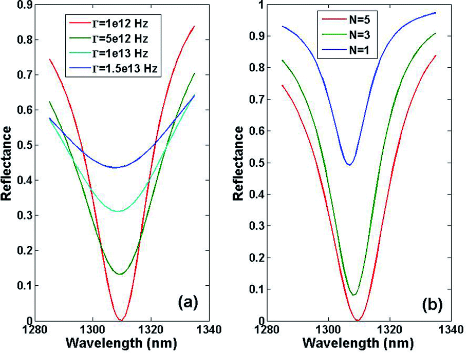
As a SPR sensor based on graphene plasmons, its performance would be affected by the quality of the graphene (especially the top graphene sheet). The quality of graphene obtained by different preparation methods varies greatly. The charge carrier mobility μ of graphene sheet generally ranges from ∼1000 to 10![[thin space (1/6-em)]](https://www.rsc.org/images/entities/char_2009.gif) 000 cm2 (V−1 s−1) in CVD graphene.37 The scattering rates corresponding to charge carrier mobilities of 1000 to 10000 cm2 (V−1 s−1) at μc = 0.596 eV are Γ = 1.5 × 10¹³ to 1.5 × 10¹² Hz (calculated using μ = (evF2)/(Γμc)46). As an example, the influences of the scattering rate Γ of the 5-atom-layer graphene sheets (top and bottom) and the atom layer number of the graphene sheets (top and bottom) with scattering rate Γ = 1.0 × 10¹² Hz on the SPR curve with a central wavelength of 1310 nm are investigated and depicted in Fig. 11. As shown in Fig. 11(a), with the increase of the scattering rate Γ of the graphene, the Rmin of the SPR curve increases rapidly and results in decreasing the extinction ratio of the SPR curve, meanwhile the FWHM increases rapidly. As shown in Fig. 11(b), with the decrease of the atom layer number of the graphene sheets, the Rmin of the SPR curve increase gradually, meanwhile the FWHM decreases gradually.
000 cm2 (V−1 s−1) in CVD graphene.37 The scattering rates corresponding to charge carrier mobilities of 1000 to 10000 cm2 (V−1 s−1) at μc = 0.596 eV are Γ = 1.5 × 10¹³ to 1.5 × 10¹² Hz (calculated using μ = (evF2)/(Γμc)46). As an example, the influences of the scattering rate Γ of the 5-atom-layer graphene sheets (top and bottom) and the atom layer number of the graphene sheets (top and bottom) with scattering rate Γ = 1.0 × 10¹² Hz on the SPR curve with a central wavelength of 1310 nm are investigated and depicted in Fig. 11. As shown in Fig. 11(a), with the increase of the scattering rate Γ of the graphene, the Rmin of the SPR curve increases rapidly and results in decreasing the extinction ratio of the SPR curve, meanwhile the FWHM increases rapidly. As shown in Fig. 11(b), with the decrease of the atom layer number of the graphene sheets, the Rmin of the SPR curve increase gradually, meanwhile the FWHM decreases gradually.
 |
| | Fig. 11 (a) SPR curves in the waveband with 1310 nm as a central wavelength for different scattering rate of both top and bottom 5-atom-layer graphene sheets; (b) SPR curves in the waveband with 1310 nm as a central wavelength for different atom layer number of both the top and the bottom graphene sheets with Γ = 1 × 10¹² Hz. | |
5. Conclusions
In conclusion, a prism-configuration tunable near-IR GSPR sensor is proposed and its wavelength interrogation sensing performance is investigated theoretically. By adjusting the chemical potential of graphene to the PR points via electrostatic gating control, the momentum mismatch between the plasmon modes in homogeneous graphene sheets and the incident near-IR radiation could be alleviated and SPR effect of graphene can be aroused within near-IR spectrum. The PR points at different wavelengths are calculated through finite element method in COMSOL and the corresponding required gate voltages are also calculated. Instead of traditional refractive index sensing, the proposed near-IR GSPR sensor can respond sensitively to the change of the chemical potential in graphene, and the CP sensitivities as well as the FWHMs of SPR curve in different wavebands within near-IR spectrum are calculated through transfer matrix method. This chemical potential sensing feature make the sensor have great potential to be used in highly sensitive biological sensing and have improved specificity. The optimal prism material, the optimal analyte layer thickness, the incident angle for working in different wavebands, and the influences of the quality (in term of the scattering rate) and atom layer number of graphene on the SPR curve are also investigated. This work provides a new thinking to detect the analyte in SPR manner which can cause chemical potential change in graphene and provides a beneficial complement to refractive index sensing SPR sensors. The tunable feature of the sensor is also helpful to achieve a balance of high sensitivity and high figure of merit in future near-IR spectral SPR sensing.
Conflicts of interest
There are no conflicts to declare.
Acknowledgements
The authors would like to acknowledge the support from the National Natural Science Foundation of China (61675092, 61575084, 61805108, 61904067); the Natural Science Foundation of Guangdong Province (2017A030313359, 2020B1515020024, 2019A1515011380); Key-Area Research and Development Program of Guangdong Province (2019B010138004); the Science and Technology Projects of Guangzhou (201803020023); The National Key and Jinan Outstanding Young Scholar Support Program (JNSBYC-2020040, JNSBYC-2020117).
Notes and references
- J. Homola, Anal. Bioanal. Chem., 2003, 377, 528–539 CrossRef CAS PubMed.
- L. Wu, H. S. Chu, W. S. Koh and E. P. Li, Opt. Express, 2010, 18, 14395–14400 CrossRef CAS PubMed.
- R. Verma, B. D. Gupta and R. Jha, Sens. Actuators, B, 2011, 160, 623–631 CrossRef CAS.
- J. B. Maurya, Y. K. Prajapati, V. Singh and J. P. Saini, Appl. Phys. A, 2015, 121, 525–533 CrossRef CAS.
- L. M. Wu, Y. Jia, L. Y. Jiang, J. Guo, X. Y. Dai, Y. J. Xiang and D. Y. Fan, J. Lightwave Technol., 2017, 35, 82–87 CAS.
- S. Aksimsek, H. Jussila and Z. P. Sun, Opt. Commun., 2018, 428, 233–239 CrossRef CAS.
- M. H. Wang, Y. Y. Huo, S. Z. Jiang, C. Zhang, C. Yang, T. Y. Ning, X. Y. Liu, C. H. Li, W. Y. Zhang and B. Y. Man, RSC Adv., 2017, 7, 47177–47182 RSC.
- L. M. Wu, J. Guo, Q. K. Wang, S. B. Lu, X. Y. Dai, Y. J. Xiang and D. Y. Fan, Sens. Actuators, B, 2017, 249, 542–548 CrossRef CAS.
- Z. N. Lin, S. J. Chen and C. Y. Lin, Sensors, 2020, 20, 2445 CrossRef CAS PubMed.
- W. Wei, J. P. Nong, Y. H. Mei, C. Y. Zhong, G. L. Lan and W. H. Hu, Sens. Actuators, B, 2018, 273, 1548–1555 CrossRef CAS.
- L. J. He, Q. Pagneux, I. Larroulet, A. Y. Serrano, A. Pesquera, A. Zurutuza, D. Mandler, R. Boukherroub and S. Szunerits, Biosens. Bioelectron., 2017, 89, 606–611 CrossRef CAS PubMed.
- C. M. Das, L. X. Kang, M. W. Chen, P. Coquet and K. T. Yong, ACS Appl. Nano Mater., 2020, 3, 10446–10453 CrossRef CAS.
- X. Xiong, Y. F. Chen, H. Wang, S. Q. Hu, Y. H. Luo, J. L. Dong, W. G. Zhu, W. T. Qiu, H. Y. Guan, H. H. Lu, J. H. Yu, J. Zhang and Z. Chen, ACS Appl. Mater. Interfaces, 2018, 10, 34916–34923 CrossRef CAS PubMed.
- Q. Wang, X. Z. Wang, H. Song, W. M. Zhao and J. Y. Jing, Opt. Laser Technol., 2020, 124, 106002 CrossRef CAS.
- H. X. Yu, Y. Chong, P. H. Zhang, J. M. Ma and D. C. Li, Talanta, 2020, 219, 121324 CrossRef CAS PubMed.
- W. Wei, J. P. Nong, G. W. Zhang, L. L. Tang, X. Jiang, N. Chen, S. Q. Luo, G. L. Lan and Y. Zhu, Sensors, 2017, 17, 2 CrossRef PubMed.
- F. Usman, J. O. Dennis, E. M. Mkawi, Y. Al-Hadeethi, F. Meriaudeau, T. L. Ferrell, O. Aldaghri and A. Sulieman, Polymers, 2020, 12, 2750 CrossRef CAS PubMed.
- A. N. Grigorenko, M. Polini and K. S. Novoselov, Nat. Photonics, 2012, 6, 749–758 CrossRef CAS.
- M. Jablan, M. Soljacic and H. Buljan, Proc. IEEE, 2013, 101, 1689–1704 CAS.
- S. Y. Huang, C. Y. Song, G. W. Zhang and H. G. Yan, Nanophotonics, 2017, 6, 1191–1204 CAS.
- L. Ju, B. S. Geng, J. Horng, C. Girit, M. Martin, Z. Hao, H. A. Bechtel, X. G. Liang, A. Zettl, Y. R. Shen and F. Wang, Nat. Nanotechnol., 2011, 6, 630–634 CrossRef CAS PubMed.
- V. W. Brar, M. S. Jang, M. Sherrott, J. J. Lopez and H. A. Atwater, Nano Lett., 2013, 13, 2541–2547 CrossRef CAS PubMed.
- Z. Y. Fang, S. Thongrattanasiri, A. Schlather, Z. Liu, L. L. Ma, Y. M. Wang, P. M. Ajayan, P. Nordlander, N. J. Halas and F. J. G. de Abajo, ACS Nano, 2013, 7, 2388–2395 CrossRef CAS PubMed.
- Z. Fei, A. S. Rodin, G. O. Andreev, W. Bao, A. S. Mcleod, M. Wagner, L. M. Zhang, Z. Zhao, M. Thiemens, G. Dominguez, M. M. Fogler, A. H. Castro Neto, C. N. Lau, F. Keilmann and D. N. Basov, Nature, 2012, 487, 82–85 CrossRef CAS PubMed.
- F. J. G. de Abajo, ACS Photonics, 2014, 1, 135–152 CrossRef.
- J. S. Gomez-Diaz and J. Perruisseau-Carrier, Opt. Express, 2013, 21, 15490–15504 CrossRef CAS PubMed.
- D. A. Iranzo, S. Nanot, E. J. C. Dias, I. Epstein, C. Peng, D. K. Efetov, M. B. Lundeberg, R. Parret, J. Osmond, J. Y. Hong, J. Kong, D. R. Englund, N. M. R. Peres and F. H. L. Koppens, Science, 2018, 360, 291–295 CrossRef PubMed.
- S. Thongrattanasiri, I. Silveiro and F. J. G. de Abajo, Appl. Phys. Lett., 2012, 100, 201105 CrossRef.
- H. G. Yan, Z. Q. Li, X. S. Li, W. J. Zhu, P. Avouris and F. N. Xia, Nano Lett., 2012, 12, 3766–3771 CrossRef CAS PubMed.
- N. Kumada, P. Roulleau, B. Roche, M. Hashisaka, H. Hibino, I. Petkovic and D. C. Glattli, Phys. Rev. Lett., 2014, 113, 266601 CrossRef CAS PubMed.
- G. X. Ni, L. Wang, M. D. Goldflam, M. Wagner, Z. Fei, A. S. Mcleod, M. K. Liu, F. Keilmann, B. Ozyilmaz, A. H. Castro Neto, J. Hone, M. M. Fogler and D. N. Basov, Nat. Photonics, 2016, 10, 244–248 CrossRef CAS.
- S. A. Mikhailov and K. Ziegler, Phys. Rev. Lett., 2007, 99, 016803 CrossRef CAS PubMed.
- A. Vakil and N. Engheta, Science, 2011, 332, 1291–1294 CrossRef CAS PubMed.
- D. Rodrigo, O. Limaj, D. Janner, D. Etezadi, F. J. G. de Abajo, V. Pruneri and H. Altug, Science, 2015, 329, 165–168 CrossRef PubMed.
- H. Hu, X. X. Yang, X. D. Guo, K. Khaliji, S. R. Biswas, F. J. G. de Abajo, T. Low, Z. P. Sun and Q. Dai, Nat. Commun., 2019, 10, 1131 CrossRef PubMed.
- R. B. Hwang, Sci. Rep., 2021, 11, 1999 CrossRef CAS PubMed.
- W. L. Gao, J. Shu, C. Y. Qiu and Q. F. Xu, ACS Nano, 2012, 6, 7806–7813 CrossRef CAS PubMed.
- C. H. Gan, Appl. Phys. Lett., 2012, 101, 111609 CrossRef.
- A. Purkayastha, T. Srivastava and R. Jha, Sens. Actuators, B, 2016, 227, 291–295 CrossRef CAS.
- Y. Huang, S. C. Zhou, H. Z. Yao and D. X. Cai, Phys. Status Solidi A, 2017, 214, 1600550 CrossRef.
- Y. Huang, S. C. Zhong, Y. C. Shen, Y. J. Yu and D. X. Cui, Nanoscale, 2018, 10, 22466–22473 RSC.
- J. S. Gomez-Diaz, C. Moldovan, S. Capdevila, J. Romeu, L. S. Bernard, A. Magrez, A. M. Lonescu and J. Perruisseau-Carrier, Nat. Commun., 2015, 6, 6334 CrossRef CAS PubMed.
- E. J. Lee, S. Y. Choi, H. Jeong, N. H. Park, W. Yim, M. H. Kim, J. K. Park, S. Son, S. Bae, S. J. Kim, K. Lee, Y. H. Ahn, K. J. Ahn, B. H. Hong, J. Y. Park, F. Rotermund and D. I. Yeom, Nat. Commun., 2015, 6, 6851 CrossRef CAS PubMed.
- W. J. Zhu, D. Neumayer, V. Perebeinos and P. Avouris, Nano Lett., 2010, 10, 3572–3576 CrossRef CAS PubMed.
- G. W. Hanson, J. Appl. Phys., 2008, 103, 064302 CrossRef.
- M. Mohsin, D. Neumaier, D. Schall, M. Otto, C. Matheisen, A. L. Giesecke, A. A. Sagade and H. Kurz, Sci. Rep., 2015, 5, 10967 CrossRef CAS PubMed.
- J. S. Gomez-Diaz, M. Esquius-Morote and J. Perruisseau-Carrier, Opt. Express, 2013, 21, 24856–24872 CrossRef CAS PubMed.
- M. Jablan, H. Buljan and M. Soljacic, Phys. Rev. B: Condens. Matter Mater. Phys., 2009, 80, 245435 CrossRef.
- N. Mohanty and V. Berry, Nano Lett., 2008, 8, 4469–4476 CrossRef CAS PubMed.
- X. C. Dong, Y. M. Shi, W. Huang, P. Chen and L. J. Li, Adv. Mater., 2010, 22, 1–5 CrossRef PubMed.
- H. Sipova and J. Homola, Anal. Chim. Acta, 2013, 773, 9–23 CrossRef CAS PubMed.
- O. Zagorodko, J. Spadavecchia, A. Y. Serrano, I. Larroulet, A. Pesquera, A. Zurutuza, R. Boukherroub and S. Szunerits, Anal. Chem., 2014, 86, 11211–11216 CrossRef CAS PubMed.
- P. Q. Gong, Y. M. Wang, X. Zhou, S. K. Wang, Y. N. Zhang, Y. Zhao, L. V. Nguyen, H. Ebendorff-Heidepriem, L. Peng, S. C. Warren-Smith and X. G. Li, Anal. Chem., 2021, 93, 10561–10567 CrossRef CAS PubMed.
- S. M. Chen, Y. Liu, Q. X. Yu and W. Peng, Sens. Actuators, B, 2021, 327, 128935 CrossRef CAS.
- S. M. Chen, C. Liu, Y. Liu, Q. Liu, M. D. Lu, S. Bi, Z. G. Jing, Q. X. Yu and W. Peng, Adv. Sci., 2020, 7, 2000763 CrossRef CAS PubMed.
- Y. Sun, H. Y. Cai, X. Qiao and X. P. Wang, Meas. Sci. Technol., 2019, 30, 125701 CrossRef CAS.
- T. Y. Xue, W. Y. Liang, Y. W. Li, Y. H. Sun, Y. J. Xiang, Y. P. Zhang, Z. G. Dai, Y. H. Duo, L. M. Wu, K. Qi, B. N. Shivananju, L. J. Zhang, X. Q. Cui, H. Zhang and Q. L. Bao, Nat. Commun., 2019, 10, 28 CrossRef CAS PubMed.
- A. B. Artyukhin, M. Stadermann, R. W. Friddle, P. Stroeve, O. Bakajin and A. Noy, Nano Lett., 2006, 6, 2080–2085 CrossRef CAS PubMed.
|
| This journal is © The Royal Society of Chemistry 2021 |
Click here to see how this site uses Cookies. View our privacy policy here. 
 Open Access Article
 This Open Access Article is licensed under a Creative Commons Attribution-Non Commercial 3.0 Unported Licence
 *ab,
Yongchun Zhongab,
Yunhan Luoab,
Jun Zhangab,
Yaofei Chen
*ab,
Yongchun Zhongab,
Yunhan Luoab,
Jun Zhangab,
Yaofei Chen