
 Open Access Article
 This Open Access Article is licensed under a
 Creative Commons Attribution 3.0 Unported Licence
First principles study of electronic and optical properties and photocatalytic performance of GaN–SiS van der Waals heterostructure
S. S. Ullaha,
M. Farooqa,
H. U. Din*bc,
Q. Alama,
M. Idreesb,
M. Bilalb and
B. Amin *b
*b
aDepartment of Physics, Hazara University, Mansehra, Pakistan
bDepartment of Physics, Abbottabad University of Science and Technology, Abbottabad, 22010, Pakistan. E-mail: haleem.uddin@yahoo.com
cDepartment of Physics, Bacha Khan University, Charsadda, Pakistan
First published on 7th October 2021
Abstract
The vertical stacking of two-dimensional materials via van der Waals (vdW) interaction is a promising technique for tailoring the physical properties and fabricating potential devices to be applied in the emerging fields of materials science and nanotechnology. The structural, electronic and optical properties and photocatalytic performance of a GaN–SiS vdW heterostructure were explored using first principles calculations. The most stable stacking configuration found energetically stable, possesses a direct staggered band gap, which is crucial for separating photogenerated charged carriers in different constituents and is efficacious for solar cells. Further, the charge transfer occurred from the SiS to GaN layer, indicating that SiS exhibits p-type doping in the GaN–SiS heterobilayer. Interestingly, a systematic red-shift was observed in the optical absorption spectra of the understudy heterobilayer system. Moreover, the conduction band edge and valence band edge of the monolayers and corresponding heterostructure were located above and below the standard redox potentials for photocatalytic water splitting, making these systems promising for water dissociation for hydrogen fuel production. The results provide a route to design the GaN–SiS vdW heterostructure for the practical realization of next-generation light detection and energy harvesting devices.
1. Introduction
Hydrogen with one electron and one proton is found in the earth's crust.1 It can be produced from other key energy sources through an energy conversion process.2 It is a secondary source of renewable energies and plays a critical role in developing environmentally friendly, low-emission, renewable and long-term energy systems.3 Hydrogen and fuel cells have a wide variety of possible applications in transportation, commerce, business, residential and portable applications. The technology of hydrogen fuel cells is currently being explored. This type of technology allows for the development of electrical energy from hydrogen, which is a pollution-free energy source that can be used to power automobiles. When hydrogen is burned, it creates water, turning it into a pollution-free fuel. However, the process of manufacturing hydrogen fuel is not particularly safe or pollution-free. Currently, natural gas is used to manufacture the majority of hydrogen, which contains carbon dioxide.4Since the earth's surface contains 71% water, hydrogen can be produced through the photocatalytic decomposition of water. Extracting hydrogen from this process is an alternative approach and highly desirable for a clean environment.5 It is a promising technology for generating renewable and clean energy, which is pollution-free with no emissions of toxic gases.6–8 Also, it has been the subject of research due to its importance in resolving energy crises and environmental issues.9 Since semiconductors have chemical and photochemical stability as well as a high absorption capacity of visible light, they can be used for water splitting. Proper valence and conduction band edge orientation make semiconductors suitable to be used for water decomposition.10
It is more difficult to choose the best photocatalyst. In general, there are two types of photocatalytic reactions: first, the uphill reaction, in which energy of photons is absorbed by the photocatalyst and transformed into chemical energy, and second, the downhill reaction, in which the photocatalyst absorbs the energy of a photon and uses it to initiate a thermodynamic reaction.11 Water splitting produces hydrogen and oxygen, which is an “uphill” reaction. If the energy of the incident light is greater than the band gap, then electrons are created in the conduction band, while holes are created in the valence band of semiconductors. Complete water decomposition occurs because of the reduction and oxidation of water molecules by electrons and holes, respectively.12 H+/H2 redox potential (0 eV) should be smaller than the conduction band minima, while the redox potential of O2/H2O (1.23 eV) must not be less than the conduction band maxima.13 In short, we can say that the band gap of the semiconductor must be greater than 1.23 eV.
Due to their novel properties14–20 and wide variety of applications in fields, such as catalysis,21 electrochemical energy storage,22 electronics,23 spintronic24,25 and photonic nanodevices,26 two-dimensional layered materials are significantly the focus of current research. The migration enhanced encapsulated growth (MEEG) method has been used to fabricate graphene-like gallium nitride (g-GaN).27 The monolayer g-GaN semiconductor has a large band gap of about 4 eV.28 Strain engineering and stacking heterostructures can enhance the properties of two-dimensional single-layer g-GaN.29–31 Furthermore, the photocatalytic application of the heterostructure of g-GaN and BlueP is possible due to the type-II band alignment.28,32,33 Also, Ren et al.32 confirmed that the g-GaN/BSe heterostructure has a type-II band alignment, which can continuously promote the separation of photogenerated charge carriers.
Two-dimensional SiS is ideal for photovoltaic applications because it has tunable electronic properties, indirect band gap, high carrier mobility, mechanically and chemically stability, and versatile anisotropic optical behavior.34 Studies showed that materials with an indirect bandgap are better for photocatalytic activity.35 SiS has a suitable bandgap value (Eg > 1.23 eV), ideal positions of the band edges and considerable optical absorption. These properties make it promising to be used in Li-ion batteries as an anode material.36 Two-dimensional materials are vertically stacked through van der Waals (vdW) interactions,37–45 which lead to the exploration of new phenomena and designing feasible optoelectronic devices such as flexible optoelectronic equipment,46 tunnel transistors47 and constructive tools.48
Three types of band alignments are type-I, type-II, or type-III in the vdW heterostructure, each having its unique application, allowing for the realization of various instruments.49 Staggered or type-II band alignment with valence band maximum (VBM) and conduction band minimum (CBM) contributed by two separate constituents will trigger optical excitation between the layers and regulates transition energy between layers. As a result, these materials are promising for the applications of solar cells, and the generation of photovoltaic power because of charge carrier separation is dominated here. Thus, in the development of advanced optoelectronic devices50 and photocatalytic applications,51 heterostructures with the staggered band alignment have drawn considerable interest. Theoretically and experimentally, lateral heterostructures have been built by in-plane stitching.52 However, producing lateral heterostructures having several junctions with high quality is still a challenge.53 In the vdW heterostructure, there is no direct chemical bond between atoms. While retaining the interlayer separation required for the vdW interaction, the lattice mismatch conditions can be relaxed to allow different layers with different lattice constants to be stacked.
In this study, we used density functional theory to look at the electronic properties of GaN–SiS vdW heterostructures in various stacking patterns. The lowest binding energy confirms the energetically stable structure among all possible configurations of the GaN–SiS heterobilayer. A direct type-II band alignment is found in the GaN–SiS vdW heterostructures. GaN–SiS vdW heterostructures also have great capability for excellent visible light absorption, which leads to applications in solar cells and optoelectronics. In addition, the understudy monolayers and heterobilayer are capable of photocatalytic water splitting, indicating their good performance of photocatalytic hydrogen fuel production.
2. Computational details
The quantum espresso54,55 is used to perform first-principles calculations based on density functional theory (DFT).56 Electronic exchange and correlation energies are determined using a type of the generalized gradient approximation (GGA)57 known as the Perdew–Burke–Ernzerhof (PBE) level.58 The Grimme's dispersion correction (DFT-D2)59 method was employed for the vdW correction. A vacuum layer of 25 Å was set in the z-direction for preventing interactions between adjacent layers. The plane wave kinetic energy cutoff was set at 500 eV. For optimization, a structure having a precision high grid of k-points was sampled via a k-grid integrated into a Brillouin zone centered at 12 × 12 × 1 and geometrically relaxed at 6 × 6 × 1. The geometric relaxation and electronic properties were carried out until the energy and forces converged to value of 10−5 eV and 0.001 eV Å−1, respectively. Also, HSE06 functional was adopted for a better understanding of the electronic band structure. The GWo method was used to measure the optical absorption spectra of the vdW heterostructure and constituent monolayers. The GWo approach was adapted, where the HSE06 single-particle energies and wave functions were used to calculate the Quasiparticle energies and solve the Bethe–Salpeter equation (TammDancoff approximation). We took into account the 10 highest valence and 10 lowest conduction bands to calculate the excitonic eigenstates.3. Results and discussion
The pristine GaN and SiS monolayers have planar and buckled graphene-like honeycomb structural geometries, as displayed in Fig. 1(a and b). The optimized lattice constants of single layer GaN and SiS are 3.25 Å and 3.29 Å, respectively. Using PBE functional, an indirect semiconducting band gap with values of 1.90 eV for GaN and 2.18 eV for SiS was obtained, as shown in Fig. 1(c and d). These results are in good agreement with the available literature,60–63 indicating the reliability of the present study (Table 1).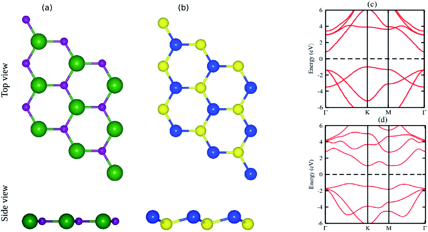 | ||
| Fig. 1 Top and side view of (a) GaN and (b) SiS monolayers, respectively. Light green, light blue, blue and yellow balls represent the Ga, N, Si and S atoms, respectively. Band structures of (c) GaN and (d) SiS monolayers. | ||
| Parameters | GaN | SiS | GaN–SiS |
|---|---|---|---|
| a (Å) | 3.25 | 3.29 | 3.27 |
| Ga–N (Å) | — | — | 1.86 |
| Si–S (Å) | — | — | 1.33 |
| Stacking-a, Eb/d (eV Å−1) | — | — | −0.115/3.542 |
| Stacking-b, Eb/d (eV Å−1) | — | — | −0.160/3.275 |
| Stacking-c, Eb/d (eV Å−1) | — | — | −0.163/3.178 |
| Stacking-d, Eb/d (eV Å−1) | — | — | −0.165/3.106 |
| Stacking-e, Eb/d (eV Å−1) | — | — | −0.152/3.301 |
| Stacking-f, Eb/d (eV Å−1) | — | — | −0.110/3.566 |
| Eg (PBE) (eV) | 1.90 | 2.18 | 1.48 |
| ECB (eV) | −1.5 | −0.14 | −0.62 |
| EVB (eV) | 0.34 | 2.04 | 0.86 |
The small lattice mismatch allowed the fabrication of the vdW heterostructure of GaN and SiS monolayers. As the layer stacking was sensitive to the orientation of individual constituents, six possible stacking configurations of the GaN–SiS vdW heterostructure are presented in Fig. 2. In stacking a(b), the Si atom is placed on top of the Ga(N)-atom and the S atom is fixed above the N(Ga)-atom. For the stacking c(d), Si-atom was positioned above the N(Ga)-atom, while S was located at the hollow site. The S-atom was placed on top of the N(Ga)-atom, while the Si-atom was fixed at the center of the hexagonal.
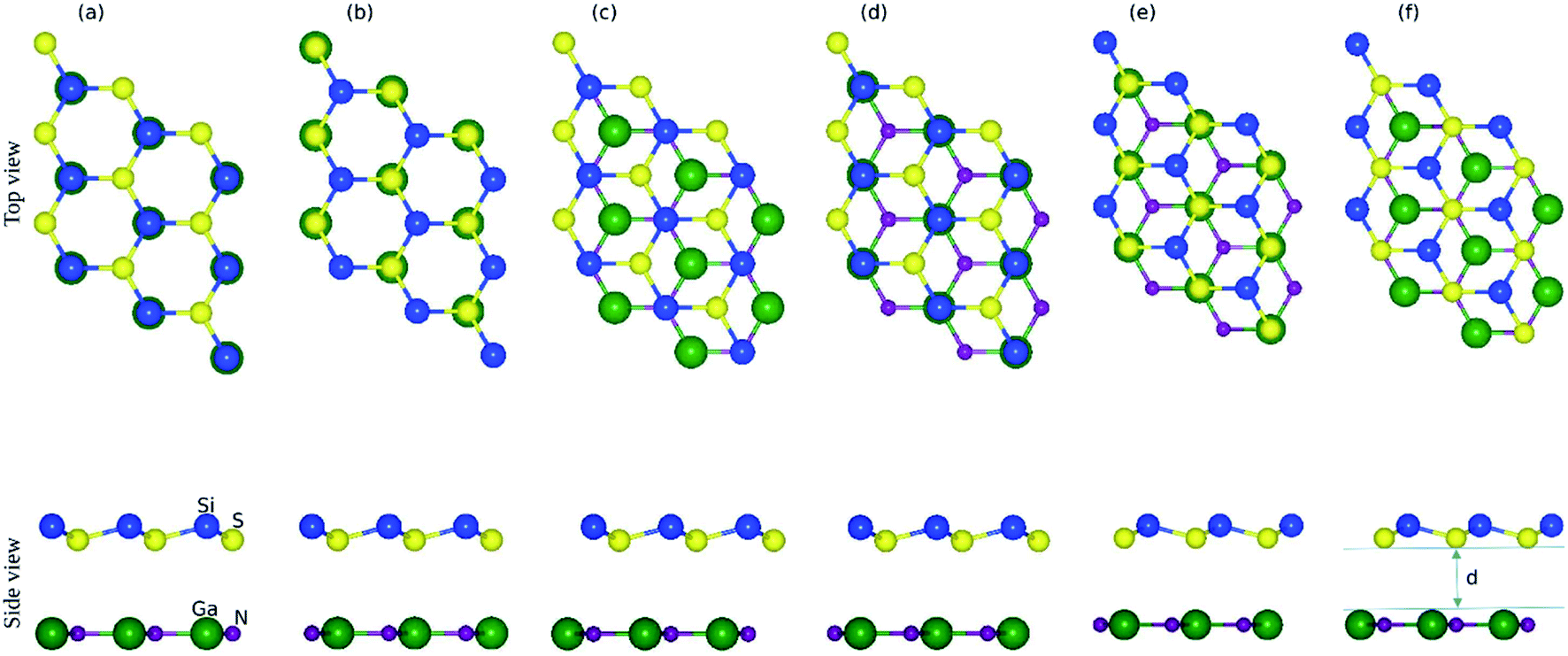 | ||
| Fig. 2 Top view and side view of six possible stacking configurations (a)–(f) of the GaN–SiS vdW heterostructure and “d” is the interlayer distance. The details of different geometrical stacking are given in the text. | ||
The difference in total energy between the heterostructure and its parent monolayers is called binding energy (Eb):
| Eb = Ehetero − Ei-monolayer − Eii-monolayer |
The calculated binding energy (interlayer distance) of GaN–SiS heterostructures for (a), (b), (c), (d), (e), and (f) patterns are −0.115 eV (3.54 Å), −0.160 eV (3.27 Å), −0.163 eV (3.17 Å), −0.165 eV (3.10 Å), −0.152 eV (3.30 Å), and −0.110 eV (3.56 Å), respectively. The stacking (d) possessed the lowest binding energy and a smaller interlayer distance “d”, indicating the energetic feasibility of stacking (d) vdW heterostructure.
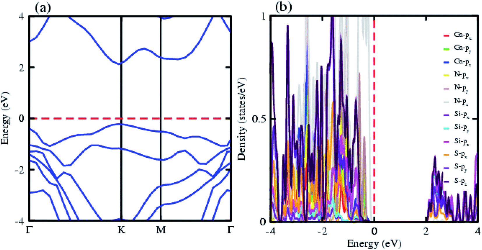
The electronic band structure of the most feasible configuration of the GaN–SiS vdW heterostructure was calculated using the PBE functional, as shown in Fig. 3(a). The GaN–SiS vdW heterostructure exhibited a direct bandgap (1.48 eV) with VBM and CBM located at the K-point of the Brillouin zone. The GaN–SiS vdW heterostructure had a smaller band gap than the pristine GaN and SiS monolayers. However, it exhibited a considerably larger band gap suitable for a photocatalytic reaction, indicating that the GaN–SiS electronic structure could be used as a visible light photocatalyst.64 For an accurate description of the band gap, we have calculated the HSE06 band structure for the GaN–SiS vdW heterostructure, which also exhibited a direct band nature with a band gap value of 2.45 eV (see Fig. 4(a)).
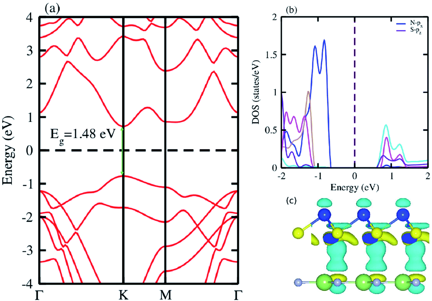 | ||
| Fig. 3 (a) Electronic band structure calculated using PBE functional; (b) partial density of states (PDOS); (c) the 3D isosurface of the charge density difference of the GaN–SiS vdW heterostructure. | ||
 | ||
| Fig. 4 (a) Electronic band structure calculated using HSE06 functional; (b) partial density of states (PDOS) of the GaN–SiS vdW heterostructure. | ||
The partial density of states of the vdW heterostructure of GaN–SiS, as presented in Fig. 3(b), is crucial for understanding the band alignment. It is clear that VBM is contributed by the py orbital of the Si atom, while CBM is mainly dominated by the px orbital of the N atom, as shown in Fig. 3(b). This confirms the type-II band alignment, which efficiently separates electrons and holes in different constitutions. Moreover, some other contributions of Ga and S atoms are also present (see Fig. 4(b)). The interlayer charge transfer is shown by the charge density difference, as displayed in Fig. 3(c). Hence, the charge density difference Δρ = ρGaN−SiS − ρGaN − ρSiS of the GaN–SiS vdW heterostructure was investigated, where ρGaN−SiS is the charge density of the heterostructure, and ρGaN and ρSiS are the charge densities of isolated GaN and SiS monolayers, respectively. The yellow color represents electron depletion, while the cyan areas show accumulation (Fig. 3(c)). The SiS layer donates electrons to the GaN layer, thus causing the SiS layer to behave as a p-doped layer. In addition, Bader charge analysis was used to estimate the total number of electrons transferred at the interface of GaN–SiS. An amount of 0.0235|e| charge was transferred from SiS to GaN layer, thus indicating p-type doping in the SiS monolayer.65,66 The charge redistribution was mainly found at the interface, which was responsible for the built-in electric field and separates photogenerated charge carries in different layers of the GaN–SiS heterostructure. This process indicates weak interaction between the GaN and SiS layers. Furthermore, we calculated the average charge density and work function of the GaN–SiS vdW heterostructure. The average charge density showed that the SiS layer has a higher potential than GaN, hence confirming the charge transfer (see Fig. 5). The calculated work function value for the GaN–SiS vdW heterostructure was 3.8 eV.
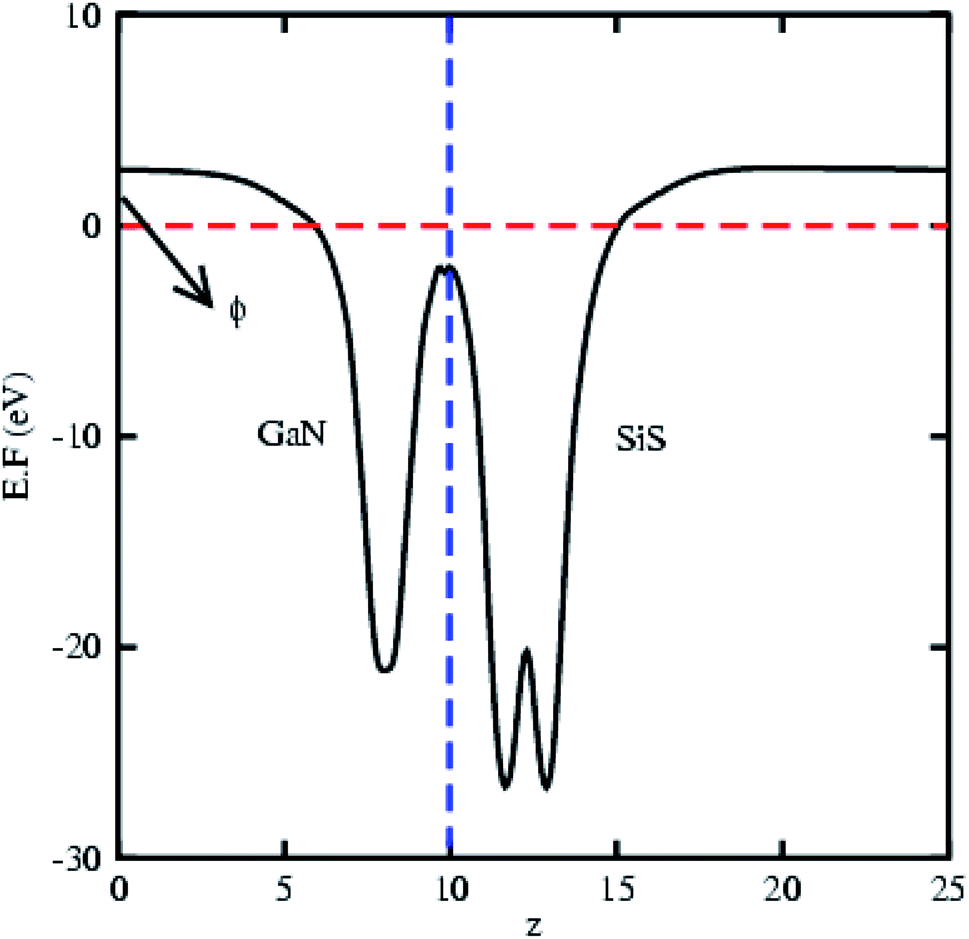 | ||
| Fig. 5 Average electrostatic potential and work function of the GaN–SiS vdW heterostructure. | ||
Further, the absorption spectra in terms of the imaginary part of the dielectric function ε2(ω) was determined for the GaN, SiS monolayers and GaN–SiS heterobilayer, as shown in Fig. 6(a–c). It is clear from Fig. 6(a and c) that exciton peaks are found at 4.97 eV and 4.65 eV in the GaN and SiS monolayers, respectively. In contrast to the parent monolayers, the excitonic peaks shifted to lower energy and were found at 1.77 eV in the GaN–SiS system. This excitonic shift will affect the effective separation of photogenerated electron–hole pairs, which directly influence the efficiency of photocatalytic water splitting. Evidently, a red-shift was found in GaN–SiS as a result of a lower band gap of the GaN–SiS heterobilayer than the corresponding monolayers;67,68 hence, GaN–SiS may be a potential candidate for optoelectronic applications. A similar trend was also found in SiC–TMDC and WS2–MoS2 heterostructures.69
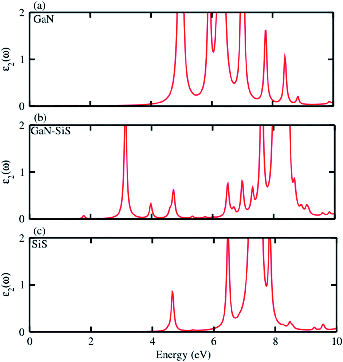 | ||
| Fig. 6 Imaginary part ε2(ω) of the dielectric function of the (a) GaN monolayer, (b) GaN–SiS vdW heterostructure and (c) isolated SiS monolayer. | ||
Mulliken electronegativity was used to study the photocatalytic behavior of the GaN–SiS heterostructures for water splitting.70,71
| ECBM = EVBM − Eg |
| EVBM = χ − Eelec + 0.5Eg |
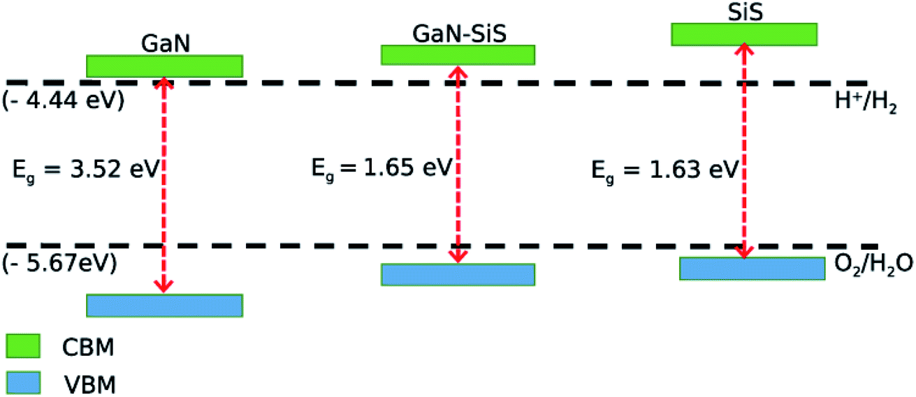 | ||
| Fig. 7 Valence and conduction band edges of GaN and SiS monolayers, and the GaN–SiS vdW heterostructure. | ||
4. Conclusion
First principles calculations were performed to explore different properties including, structural, electronic, optical and photocatalytic properties of the GaN–SiS vdW heterostructure. The most feasible configuration was energetically stable. Both the GaN and SiS possessed indirect semiconducting band gap nature. The understudy heterobilayer exhibited direct type-II band alignment, and the photogenerated electrons and holes were spatially separated, which is crucial for solar cell device applications. The charges were transferred from SiS to the GaN monolayer, and SiS became p-type doping in the GaN–SiS vdW heterostructure. Furthermore, a systematically red-shift with lower energy excitonic transition was found in the corresponding vdW heterostructure. Interestingly, the valence band and conduction band edges of both heterobilayer and pristine monolayers are were located above and below the standard redox potentials, for photocatalytic water decompositions, which suggested that the understudy monolayers and heterobilayer systems were meant for water dissociation under a solar spectrum. The findings open up an avenue for designing new devices based on the GaN–SiS heterobilayer for promising optoelectronic and photocatalytic water splitting to produce hydrogen as a renewable energy source.Conflicts of interest
There are no conflicts of interest to declare.References
- R. Aversa, V. Petrescu, A. Apicella and I.-T. Petrescu, Am. J. Appl. Sci., 2016, 9, 1189 CrossRef.
- T. N. Veziroǧglu and S. Sahin, Energy Conv.Manag., 2008, 49, 1820–1831 CrossRef.
- M. Balat, Int. J. Hydrog. Energy, 2008, 33, 4013–4029 CrossRef CAS.
- S. I. Ngo, Y.-I. Lim, W. Kim, D. J. Seo and W. L. Yoon, Appl. Energy, 2019, 236, 340–353 CrossRef CAS.
- P. Edwards, V. Kuznetsov, W. David and N. Brandon, Energy Policy, 2008, 36, 4356–4362 CrossRef.
- A. Fujishima and K. Honda, Nature, 1972, 238, 37–38 CrossRef CAS PubMed.
- F. E. Osterloh, Chem. Mater., 2008, 20, 35–54 CrossRef CAS.
- X. Hu, G. Li and J. C. Yu, Langmuir, 2010, 26, 3031–3039 CrossRef CAS PubMed.
- M. R. Axet, J. Durand, M. Gouygou and P. Serp, Adv. Organ. Chem., Acad. Press, 2019, 71, 53–174 CAS.
- C. Chowdhury, S. Karmakar and A. Datta, J. Phys. Chem. C, 2017, 121, 7615–7624 CrossRef.
- M. Matsuoka, M. Kitano, M. Takeuchi, K. Tsujimaru, M. Anpo and J. M. Thomas, Cataly. Tod., 2007, 122, 51–61 CrossRef CAS.
- V. Artero, M. Chavarot-Kerlidou and M. Fontecave, Angew. Chem., Int. Ed., 2011, 50, 7238–7266 CrossRef CAS PubMed.
- A. Kudo, Pur. Appl. Chem., 2007, 79, 1917–1927 CAS.
- A. Bafekry, C. Stampfl, M. Ghergherehchi and S. F. Shayesteh, Carbon, 2020, 157, 371–384 CrossRef CAS.
- A. Bafekry, M. Neek-Amal and F. Peeters, Phys. Rev. B, 2020, 101, 165407 CrossRef CAS.
- A. Bafekry, C. Stampfl and F. M. Peeters, Scien. Rep., 2020, 10, 1–15 CrossRef PubMed.
- A. Bafekry, M. Ghergherehchi and S. F. Shayesteh, Phys. Chem. Chem. Phys., 2019, 21, 10552–10566 RSC.
- A. Bafekry, Phys. E: Low-dimen. Sys. Nanostruc., 2020, 118, 113850 CrossRef CAS.
- A. Bafekry, C. Stampfl and F. M. Peeters, Phy. Stat. Sol.b, 2020, 257, 2000182 CrossRef CAS.
- A. Bafekry, B. Akgenc, M. Ghergherehchi and F. Peeters, J. Phys.: Cond. Matt., 2020, 32, 355504 CrossRef CAS PubMed.
- D. Deng, K. S. Novoselov, Q. Fu, N. Zheng, Z. Tian and X. Bao, Nat. Nanotechnol., 2016, 11, 218–230 CrossRef CAS PubMed.
- E. Pomerantseva and Y. Gogotsi, Nat. Energ., 2017, 2, 17089 CrossRef CAS.
- K. Ren, M. Sun, Y. Luo, S. Wang, J. Yu and W. Tang, Appl. Surf. Sci., 2019, 476, 70–75 CrossRef CAS.
- Q.-F. Yao, J. Cai, W.-Y. Tong, S.-J. Gong, J.-Q. Wang, X. Wan, C.-G. Duan and J. H. Chu, Phys. Rev. B, 2017, 95, 165401 CrossRef.
- S. Wang and J. Yu, J. Supercon. Nov. Mag., 2018, 31, 2789–2795 CrossRef CAS.
- M. Zhang, X.-X. Wang, W.-Q. Cao, J. Yuan and M.-S. Cao, Adv. Opt. Mater., 2019, 7, 1900689 CrossRef CAS.
- Z. Y. Al Balushi, K. Wang, R. K. Ghosh, R. A. Vilá, S. M. Eichfeld, J. D. Caldwell, X. Qin, Y.-C. Lin, P. A. DeSario and G. Stone, et al., Nat. Mater., 2016, 15, 1166 CrossRef CAS PubMed.
- M. Sun, J.-P. Chou, Q. Ren, Y. Zhao, J. Yu and W. Tang, Appl. Phys. Lett., 2017, 110, 173105 CrossRef.
- H. Shu, X. H. Niu, X. J. Ding and Y. Wang, Appl. Surf. Sci., 2019, 479, 475–481 CrossRef CAS.
- H. Shu, M. Zhao and M. Sun, ACS Appl. Nano Mater, 2019, 2(10), 6482–6491 CrossRef CAS.
- H. Shu, Mater. Scie. Eng. B, 2020, 261, 114672 CrossRef CAS.
- K. Ren, S. Wang, Y. Luo, Y. Xu, M. Sun, J. Yu and W. Tang, RSC Adv., 2019, 9, 4816 RSC.
- K. Ren, J. Yu and W. Tang, J. Appl. Phys., 2019, 126, 065701 CrossRef.
- J. H. Yang, Y. Zhang, W. J. Yin, X. G. Gong, B. I. Yakobson and S. H. Wei, Nano Lett., 2016, 16(2), 1110–1117 CrossRef CAS PubMed.
- P. Zhang, J. Zhang and J. Gong, Chem. Soc. Rev., 2014, 43(13), 4395–4422 RSC.
- K. Ren, S. Wang, Y. Luo, Y. Xu, M. Sun, J. Yu and W. Tang, RSC Adv., 2019, 9(9), 4816–4823 RSC.
- M. Idrees, H. U. Din, S. U. Rehman, M. Shafiq, Y. Saeed, H. D. Bui, C. V. Nguyen and B. Amin, Phys. Chem. Chem. Phys., 2020, 22(18), 10351–10359 RSC.
- B. Amin, T. P. Kaloni, G. Schreckenbach and M. S. Freund, Appl. Phys. Lett., 2016, 108, 063105 CrossRef.
- A. Bafekry, C. Stampfl and M. Ghergherehchi, Nanotechnology, 2020, 31, 295202 CrossRef CAS PubMed.
- A. Bafekry, M. Yagmurcukardes, B. Akgenc, M. Ghergherehchi and C. V. Nguyen, J. Phy. D: Appl. Phy., 2020, 53, 355106 CrossRef CAS.
- S. Wang, C. Ren, H. Tian, J. Yu and M. Sun, Phys. Chem. Chem. Phys., 2018, 20, 13394–13399 RSC.
- S. Wang, H. Tian, C. Ren, J. Yu and M. Sun, Sci. Rep., 2018, 8, 1–6 Search PubMed.
- K. Ren, S. Wang, Y. Luo, J.-P. Chou, J. Yu, W. Tang and M. Sun, J. Phy. D: Appl. Phy., 2020, 53, 185504 CrossRef CAS.
- Y. Luo, S. Wang, K. Ren, J.-P. Chou, J. Yu, Z. Sun and M. Sun, Phys. Chem. Chem. Phys., 2019, 21, 1791–1796 RSC.
- S. Wang, J.-P. Chou, C. Ren, H. Tian, J. Yu, C. Sun, Y. Xu and M. Sun, Sci. Rep., 2019, 9, 1–7 Search PubMed.
- O. Lopez-Sanchez, E. Alarcon Llado, V. Koman, A. Fontcuberta i Morral, A. Radenovic and A. Kis, ACS Nano, 2014, 8, 3042–3048 CrossRef CAS PubMed.
- T. Roy, M. Tosun, X. Cao, H. Fang, D.-H. Lien, P. Zhao, Y.-Z. Chen, Y.-L. Chueh, J. Guo and A. Javey, ACS Nano, 2015, 9, 2071–2079 CrossRef CAS PubMed.
- Z. Yu, Y. Pan, Y. Shen, Z. Wang, Z.-Y. Ong, T. Xu, R. Xin, L. Pan, B. Wang, L. Sun, J. Wang, G. Zhang, Y. W. Zhang, Y. Shi and X. Wang, Nat. Commun., 2014, 5, 5290 CrossRef CAS PubMed.
- V. O. Özçelik, J. G. Azadani, C. Yang, S. J. Koester and T. Low, Phys. Rev. B, 2016, 94, 035125 CrossRef.
- P. Rivera, J. R. Schaibley, A. M. Jones, J. S. Ross, S. Wu, G. Aivazian, P. Klement, K. Seyler, G. Clark, N. J. Ghimire, J. Yan, D. G. Mandrus, W. Yao and X. Xu, Nat. Commun., 2015, 6, 6242 CrossRef CAS PubMed.
- X. Hong, J. Kim, S.-F. Shi, Y. Zhang, C. Jin, Y. Sun, S. Tongay, J. Wu, Y. Zhang and F. Wang, Nat. Nanotech., 2014, 9, 682–686 CrossRef CAS PubMed.
- Y. Gong, J. Lin, X. Wang, G. Shi, S. Lei, Z. Lin, X. Zou, G. Ye, R. Vajtai and B. I. Yakobson, et al., Nat. Mater., 2014, 13, 1135–1142 CrossRef CAS PubMed.
- P. K. Sahoo, S. Memaran, Y. Xin, L. Balicas and H. R. GutiÃl'rrez, Nature, 2018, 553, 63–67 CrossRef CAS PubMed.
- G. Kresse, J. Non-Cryst. Sol., 1995, 192–193, 222–229 CrossRef.
- G. Kresse and J. Furthmüller, Phys. Rev. B: Condens. Matter Mater. Phys., 1996, 54, 11169–11186 CrossRef CAS PubMed.
- W. Kohn and L. J. Sham, Phys. Rev., 1965, 140, A1133–A1138 CrossRef.
- J. P. Perdew, K. Burke and M. Ernzerhof, Phys. Rev. Lett., 1996, 77, 3865–3868 CrossRef CAS PubMed.
- J. Heyd, G. E. Scuseria and M. Ernzerhof, J. Chem. Phys., 2003, 118, 8207–8215 CrossRef CAS.
- S. Grimme, J. Comput. Chem., 2006, 27, 1787–1799 CrossRef CAS PubMed.
- A. Mogulkoc, Y. Mogulkoc, M. Modarresi and B. Alkan, Phys. Chem. Chem. Phys., 2018, 20(44), 28124–28134 RSC.
- H. U. Din, M. Idrees, T. A. Alrebdi, C. V. Nguyen and B. Amin, Comp. Mat. Sci., 2019, 164, 166–170 CrossRef CAS.
- R. Yuan, J. A. Napoli, C. Yan, O. Marsalek, T. E. Markland and M. D. Fayer, ACS Cent. Sci., 2019, 5, 1269–1277 CrossRef CAS PubMed.
- P. Rivera, J. R. Schaibley, A. M. Jones, J. S. Ross, S. Wu, G. Aivazian, P. Klement, K. Seyler, G. Clark and N. J. Ghimire, et al., Nat. Commun., 2015, 6, 1–6 Search PubMed.
- Y. Li, Y.-L. Li, B. Sa and R. Ahuja, Cataly. Sci. Techn., 2017, 7, 545–559 RSC.
- B.-J. Wang, X.-H. Li, R. Zhao, X.-L. Cai, W.-Y. Yu, W.-B. Li, Z.-S. Liu, L.-W. Zhang and S.-H. Ke, J. Mater. Chem. A, 2018, 6, 8923–8929 RSC.
- H. U. Din, M. Idrees, A. Albar, M. Shafique, I. Ahmad, C. V. Nguyen and B. Amin, Phys. Rev. B, 2019, 100, 165425 CrossRef CAS.
- H. Hsueh, G. Guo and S. G. Louie, Phys. Rev. B: Condens. Matter Mater. Phys., 2011, 84, 085404 CrossRef.
- H. Din, M. Idrees, G. Rehman, C. V. Nguyen, L.-Y. Gan, I. Ahmad, M. Maqbool and B. Amin, Phys. Chem. Chem. Phys., 2018, 20, 24168–24175 RSC.
- S. Tongay, W. Fan, J. Kang, J. Park, U. Koldemir, J. Suh, D. S. Narang, K. Liu, J. Ji and J. Li, et al., Nano letters, 2014, 14, 3185–3190 CrossRef CAS PubMed.
- J. Liu, X. Fu, S. Chen and Y. Zhu, Appl. Phys. Lett., 2011, 99, 191903 CrossRef.
- H. L. Zhuang and R. G. Hennig, Phys. Rev. B: Condens. Matter Mater. Phys., 2013, 88, 115314 CrossRef.
- V. Chakrapani, J. C. Angus, A. B. Anderson, S. D. Wolter, B. R.Stoner and G. U. Sumanasekera, Science, 2007, 318, 1424–1430 CrossRef CAS PubMed.
| This journal is © The Royal Society of Chemistry 2021 |