
 Open Access Article
 This Open Access Article is licensed under a
 Creative Commons Attribution 3.0 Unported Licence
Atmospheric pressure chemical vapor deposition growth of vertically aligned SnS2 and SnSe2 nanosheets†
Ayrton Sierra-Castillo *a,
Emile Hayeb,
Selene Acostac,
Raul Arenaldef,
Carla Bittencourtc and
Jean-François Colomera
*a,
Emile Hayeb,
Selene Acostac,
Raul Arenaldef,
Carla Bittencourtc and
Jean-François Colomera
aResearch Group on Carbon Nanostructures (CARBONNAGe), University of Namur, 5000 Namur, Belgium. E-mail: ayrton.sierracastillo@gmail.com
bLaboratoire d'Analyse par Réactions Nucléaires (LARN), Namur Institute of Structured Matter (NISM), University of Namur, 5000 Namur, Belgium
cChimie des Interactions Plasma–Surface (ChIPS), Research Institute for Materials Science and Engineering, Université de Mons, 7000 Mons, Belgium
dInstituto de Nanociencia y Materiales de Aragon (INMA), CSIC-Universidad de Zaragoza, 50009 Zaragoza, Spain
eLaboratorio de Microscopias Avanzadas (LMA), Universidad de Zaragoza, 50018 Zaragoza, Spain
fARAID Foundation, 50018 Zaragoza, Spain
First published on 11th November 2021
Abstract
Laminated metal dichalcogenides are candidates for different potential applications ranging from catalysis to nanoelectronics. However, efforts are still needed to optimize synthesis methods aiming to control the number of layers, morphology, and crystallinity, parameters that govern the properties of the synthesized materials. Another important parameter is the thickness and the length of the samples with the possibility of large-scale growth of target homogeneous materials. Here, we report a chemical vapor deposition method at atmospheric pressure to produce vertically aligned tin dichalcogenide based-materials. Tin disulfide (SnS2) and tin diselenide (SnSe2) vertically aligned nanosheets have been synthesized and characterized by different methods showing their crystallinity and purity. Homogenous crystalline 2H-phase SnS2 nanosheets with high purity were synthesized with vertical orientation on substrates; sulfur vacancies were observed at the edges of the sheets. Similarly, in the crystalline 2H phase SnSe2 nanosheets selenium vacancies were observed at the edges. Moreover, these nanosheets are larger than the SnS2 nanosheets, show lower nanosheet homogeneity on substrates and contamination with selenium atoms from the synthesis was observed. The synthesized nanomaterials are interesting in various applications where the edge accessibility and/or directionality of the nanosheets play a major role as for example in gas sensing or field emission.
Introduction
Two-dimensional (2D) layered nanostructures have received increasing interest due to their unique nanoscale phenomena and their potential applications ranging from electronics and energy to catalysis. In the last decade, different 2D layered dichalcogenides, such as molybdenum disulfide (MoS2),1 tungsten disulfide (WS2),2 molybdenum diselenide (MoSe2),3 tungsten diselenide (WSe2),4 tin disulfide (SnS2)5 and tin diselenide (SnSe2)6 have been widely studied. The interest in these nanomaterials was trigged by their potential applications in field-effect transistors (FETs),7 photodetectors,8 solar cells,9,10 and gas sensors.11,12 SnS2 and SnSe2 have a similar configuration as MoS2, in which a Sn layer is sandwiched between two S or Se layers to form a “three-layer” structure (one metal atom between two chalcogenide atoms, covalently bonded, and the layers are linked between them by van der Waals forces).Tin disulfide (SnS2) and tin diselenide (SnSe2) belong to the family IVA–VIA group, which are earth-abundant and environment-friendly materials, and due to their low cost, they present a considerable advantage for nanoelectronics and optoelectronics. There are several recently reports on the optical, electrical, and photoelectric properties of SnS2 nanomaterials.13,14 SnS2 is a broadband gap semiconductor with band energy gap of 2.2 eV.14 In addition, SnS2 has a higher theoretical capacity, compared to other 2D materials, such as MoS2 and WS2.15 All these properties make SnS2 a promising candidate for FETs, integrated logic circuits, photodetectors; energy storage materials and solar cells. With a direct band gap of 1.4 eV,15 SnSe2 is attractive in the fields of nanoelectronics and optoelectronics, but also due to its structure and low cost, it is a strong candidate for sensing applications.16
Therefore, the controllable growth of these materials is the first and critical step for their device applications, to have a reproductible control of the structure, including the number of layers, the crystallographic phase composition, or/and film morphology. Previous studies have already demonstrated that these 2D materials can be prepared using chemical17 or mechanical18 exfoliation, spray pyrolysis,19 thermal evaporation,20 hydrothermal method12,21,22 and chemical vapor deposition (CVD).23 In general, the research in this area focus on the synthesis of monolayer domains of controlled size, whose properties are interesting for applications in electronics.24 CVD has proven to be an effective method for synthesizing this type of material where control of the number of layers is important, however CVD also allows the control of the material morphology opening up new applications. Previously with CVD, high-quality 2D layered nanostructures, such as MoS2 (ref. 25) and WSe2 (ref. 26) were synthesized vertically aligned to the substrate, with possible applications as gas sensors27 or field emission sources.28
In the CVD method, different experimental geometries and strategies can be used leading to nanomaterials with different morphology, crystallinity (phase), crystal size, etc.29 This is also true for the CVD growth of metal dichalcogenides, here taking advantage of this unique characteristic of the CVD growth, the focus is done on tin dichalcogenide materials. The CVD strategy used is based on the co-evaporation of two precursors one for the metal, the other for the chalcogenide. Therefore, using sulfur and tin powers for the synthesis of SnS2 hexagonal nanosheets are obtained.30 While, when sulfur and SnS2 powder, hexagonal and truncated triangular nanosheets are observed.31 These latter examples concern the in-plane growth of the 2D materials, however other morphologies have been reported also based on CVD with co-evaporation. As well, vertically aligned SnS2 nanosheets with the hexagonal 2H phase, have been synthesized using S and SnI2 powder5 or SnCl4·5H2O (ref. 32) as tin source. These same strategies were used to produce Se-based nanomaterials, for in-plane growth, using Se with SnI2, few-layers SnSe2 were formed on mica substrate with triangular33 or hexagonal34 crystal shapes. Using different sources, i.e. Se and SnO2 powder hexagonal crystals were obtained.35 Within this perspective, using SnSe as tin precursor, the crystallographic phase was fine controlled by tuning the control by synthesis temperature.36 Furthermore, using diethethyl selenide with SnCl4 as precursor for the synthesis, a vertical preferential growth of SnSe2 was observed.37
A different CVD strategy for the synthesis of metal dichalcogenides is direct sulfurization27 or selenization38 of metal films. The deposition of a metallic film of controlled thickness allows to know precisely where the nanocrystals will be synthesized, avoiding non-uniform dispersion and distribution of the nanosheets in the case of evaporation of metal precursors with chalcogenide as explained previously.39 Another advantage of this strategy is the possibility to control the nanosheets height – when they are vertically aligned – with the well-defined film thickness.40 However, it is difficult, if not impossible, to synthesize monolayer crystal domains using this strategy because of the adapted thickness of the film and the high temperature used causing the film dewetting. Finally, for the synthesis of vertically aligned nanosheets, this strategy seems to be a reproducible and can be used in the synthesis of many metal dichalcogenides-based materials.27,38,40 The metallic films with controlled thickness can be deposited using different physical methods such as e-beam evaporation,27 magnetron sputtering,41 etc. In this work, we propose to apply this strategy for the first time to the best of our knowledge for the synthesis of vertically-aligned SnS2 and SnSe2 by rapid sulfurization and selenization, respectively, using the atmospheric pressure CVD (APCVD) technique. The structural, morphological and chemical characterization of the nanostructures, performed by X-ray diffraction, electron microscopies, Raman and X-ray photoelectron spectroscopies confirm the crystallinity and purity of the materials.
Materials and methods
Materials
The commercial products, namely the Sn target (purity 99.95%) was purchased from Micro to Nano, S (purity 99%) and Se powder (purity 99%) were purchased from Alfa Aesar, all the products were used as received.Synthesis of SnS2 and SnSe2 nanosheets
The SnS2 and SnSe2 nanosheets were synthesized via atmospheric pressure CVD. A 50 nm thick Sn film was deposited on a sapphire substrate by direct current magnetron sputtering (sputter current 100 mA), using a commercial sputter deposition system (Quorum Q15T/ES) in an Argon (99.9995%) atmosphere. A pure Sn target with a 57 mm diameter was used, and the substrates were placed on a rotating holder with a 90 mm target. The pressure of the argon in the deposition chamber was 1 × 10⁻³ mbar. The Sn film thickness was monitored using a quartz microbalance mounted in the deposition chamber system.Before the synthesis, the Sn film was oxidized at 300 °C with air flow using atmospheric pressure. The influence of the Sn oxidation is presented in the Fig. S1.† The sulfurization was performed on a quartz tube (reactor). Firstly, the Sn film on the sapphire substrate was introduced into the reactor with the S powder, and this was placed in two predefined zones of the tube (0.210 g was used in each zone) in order to be in the correct temperature zones when the reactor was inserted into the furnace. The S powder was used without any further purification. The reactor was flushed for one hour to remove (reduce the amount of) oxygen, using a 0.745 L min−1 argon flow outside of the furnace, prior to the sulfurization process. After that, the reactor was put inside of the furnace and the argon flow reduced to 0.070 L min−1. As in a typical sulfurization process, the reactor is moved in order to place the S powder at 550 °C into the oven, another S powder is placed close to the Sn film sample at the same right temperature zone, with the argon flow for 30 minutes (Fig. S2†). After the reaction, the quartz tube was removed from the reactor and was cooled with the argon flow for 1 h. In Fig. S3 and S4† different synthesis temperatures and gas flows are presented to show the effect of changing conditions for the synthesis of our material, respectively.
For the second material, a selenization was performed following the previous details described for sulfurization. However, instead of S, we used Se powder (0.350 g was used in each zone). The reactor was flushed for one hour to remove (reduce) oxygen, using a 0.745 L min−1 argon flow outside of the furnace, prior to the sulfurization process. After that, the reactor was put inside of the furnace and the argon flow changed to 0.010 L min−1. A 0.010 L min−1 H2 flow was inserted during this synthesis to help with the reaction. The presence of a strong reducer, such as the H2, is mandatory for the selenization reaction, in contrast with the sulfurization reaction.26 In a typical selenization process and as in the sulfurization reaction, the reactor is moved in order to place the Se powder at 450 °C into the oven, another Se powder is placed close to the Sn film sample at the same right temperature zone, with the argon and hydrogen flow for 30 minutes (Fig. S5†). After the reaction, the H2 flow was stopped, and the quartz tube was removed from the reactor and was cooled with the argon flow for 1 h. Similar as in the case of the first material, Fig. S6 and S7† show the influence of the synthesis temperature and gas flow during the synthesis process.
Characterization techniques
Scanning electron microscopy (SEM) analyses were conducted on a JEOL 7500F microscope operating at 15 kV. Transmission electron microscopy studies were carried out on a TECNAI T20 microscope working under 200 kV for bright-field images and electron diffraction and on an aberration-corrected FEI Titan Low-base microscope for scanning TEM. This STEM instrument was operated at 80 kV and is equipped with an Oxford silicon-drift-detector (SDD) for X-ray spectroscopic (EDS) analyses. The SnS2 and SnSe2 nanosheets were examined using a micro-Raman system (Senterra Bruker Optik GmbH) with a 3 cm−1 resolution, using a laser excitation laser source (532 nm wavelength), and a laser power of 2 and 5 mW, respectively. The structure of the sample has been investigated by X-ray diffraction (XRD) using a Panalytical X'Pert PRO diffractometer (Cu Kα radiation, Bragg–Brentano geometry). The chemistry of the SnS2 and SnSe2 nanosheets was studied with X-ray photoelectron spectroscopy (XPS) using an Escalab 250i Thermo Fisher Scientific™ instrument (consisting of a monochromatic Al Kα X-ray source at 1486.68 eV and working at 13.9 keV and 5.2 mA). The base pressure during spectra acquisition was better than 1010 mbar. The O 1s, Sn 3d, S 2p and Se 3d core level spectra are recorded with a pass energy of 20 eV, with 20 scans, in sequential mode, with a spot size of 250 × 250 μm2. The calibration and linearity of the binding energy scale is regularly determined by Cu 2p3/2, Ag 3d5/2 and Au 4f7/2 energies. With the selected scan parameters and a pass energy of 25 eV, the energy resolution was ≈0.7 eV measured on the FWHM of the Ag 3d5/2. A flood gun is used during the analysis to limit the charge shifting, which has been further checked by the position of the valence band minimum. No charge shift is applied to the spectra. The authors are aware of the recent warnings about XPS analysis on insulating samples.42–44Results
Fig. 1 and 2 show the SEM images recorded after the sulfurization and selenization of 50 nm of Sn deposited on sapphire substrate. For the two different materials, SnS2 and SnSe2 nanosheets can be observed. The low-magnification images in Fig. 1a and b reveal a large amount of SnS2 nanoplatelets that are uniformly distributed on the sapphire substrate. The high magnification image (Fig. 1c) shows SnS2 nanoplatelets, with an average length of 500–600 nm and a thickness of 30–35 nm, have a well-defined shape with sharp edges. The difference between these three images is the magnification. The homogeneity of the sample (Fig. 1a) can be observed (Fig. 1b and c). Fig. 1d shows the cross section of the sample. The image was taken at till angle of 62°, the presence of SnS2 nanosheets with vertical orientation can be observed.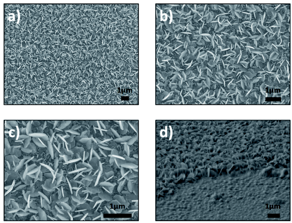 | ||
| Fig. 1 SEM images of synthesized products for vertically aligned SnS2 nanosheets, (a–c) top view and (d) cross section (62°). | ||
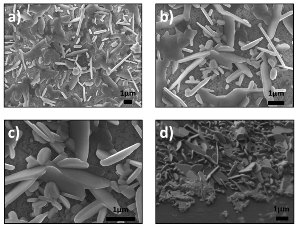 | ||
| Fig. 2 SEM images of synthesized products for vertically aligned SnSe2 nanosheets, (a–c) top view and (d) cross section (45°). | ||
Fig. 2a and b show the SnSe2 nanosheets with different orientations (vertical and horizontal). In addition, these nanosheets present a variety of sizes and shapes. This is not the case for the SnS2 samples, which are more homogeneous. The high magnification of Fig. 2c reveals the average length of the SnSe2 nanosheets (∼2.5 μm) as well as their thickness (ranging between 50 and 100 nm). The cross section of the sample at till angle of 45° confirms the different orientations of the SnSe2 nanosheets (Fig. 2d).
For further information on morphology, the as-synthesized SnS2 nanosheets were characterized using TEM (Fig. 3 and 4). The Fig. 3a and b shows representative images of nanosheets exhibiting the layered structure with a typical interlayer distance of 0.59 nm corresponding to the (001) crystal planes. Fig. 3c shows a low magnification TEM image of a single nanosheet with the corresponding selected area diffraction (SAED) pattern in the inset. This SAED pattern exhibits well-defined and sharp spots in a hexagonal geometry, indicating a hexagonal crystal structure and the single-crystal nature of the observed nanosheet. A magnified region of this nanosheet is displayed in Fig. 3d. The lattice fringes with spacing to 0.32 nm are clearly observed and they correspond to the (100) crystal planes. This distance confirms also the hexagonal phase of the nanosheets.45,46
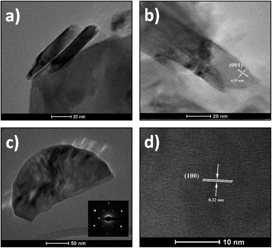 | ||
| Fig. 3 (a and b) TEM images of layered structures of SnS2 nanosheets. (c) Low magnification image of a single nanosheet with SAED pattern in inset and (d) high-resolution TEM image of the crystal showing the (001) crystal planes. | ||
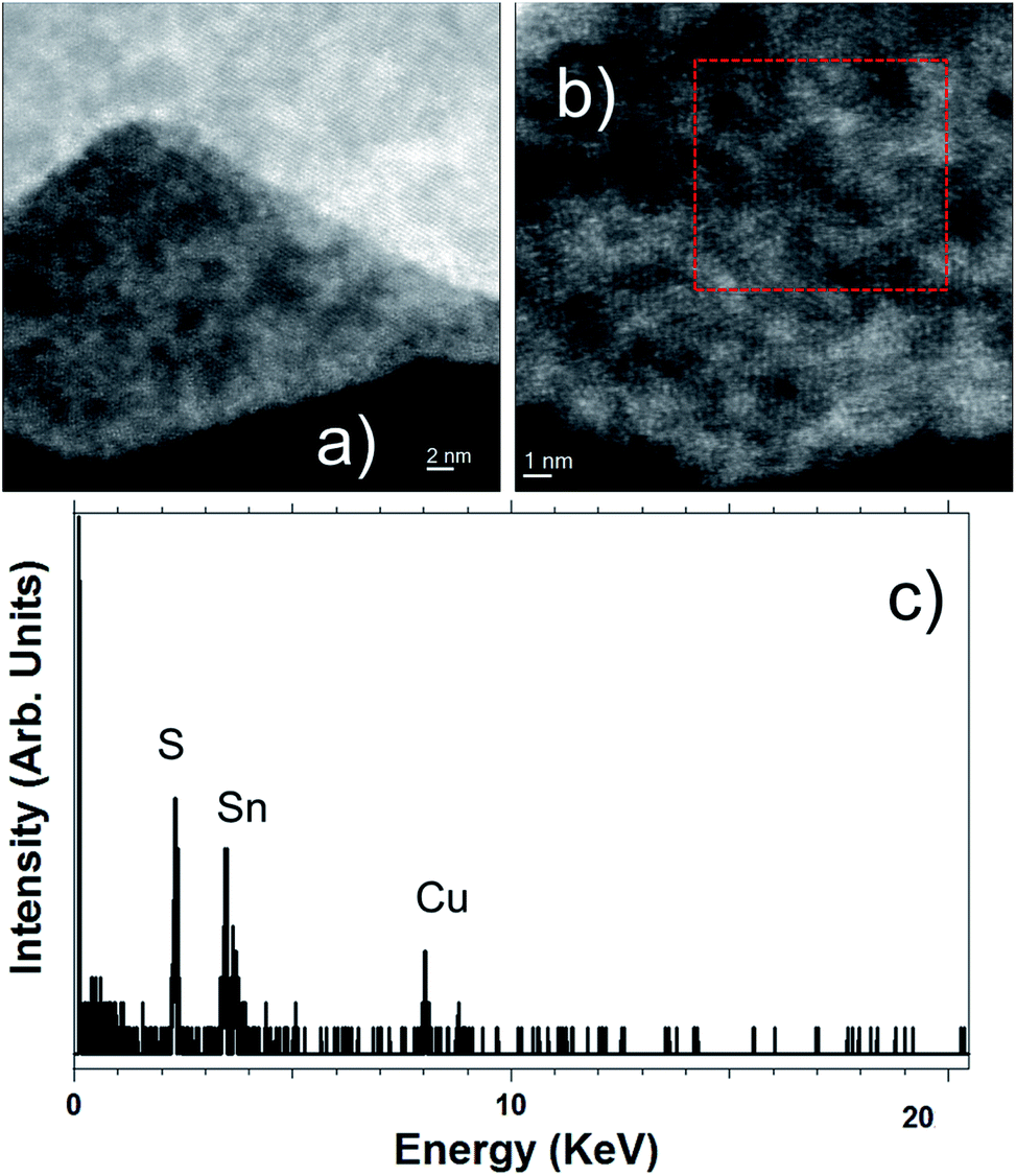 | ||
| Fig. 4 (a and b) HAADF-STEM images of SnS2 nanosheets. (c) EDS spectrum recorded in the red highlighted area of Fig. 3b. | ||
Fig. 4a and b show two high-angle annular dark-field (HAADF) STEM micrographs of two different SnS2 nanosheets, revealing the high crystallinity of these flakes. EDS analyses performed on these materials confirm the high purity of these flakes and the ratio of 2 for S/Sn (see Fig. 4c).
Concerning the SnSe2 nanosheets, they have been characterized by TEM in the same way as the SnS2 nanosheets and the results are shown in Fig. 5 and 6. The layered structure of nanosheets can be observed in Fig. 5a with an interlayer spacing of 0.61 nm, which matches to the lattice spacing of (001) planes of hexagonal SnSe2 (ref. 47) (the corresponding SAED pattern in inset Fig. 5a is consistent with HRTEM image). Fig. 5b presents a high-resolution TEM image of nanosheet with well visible lattice fringes with a spacing of 0.33 nm that can be assigned to the (100) planes of the SnSe2. The SAED pattern is in inset of a single nanosheet in the (001) direction confirms the formation of the hexagonal phase of SnSe2 and the crystal structure.48
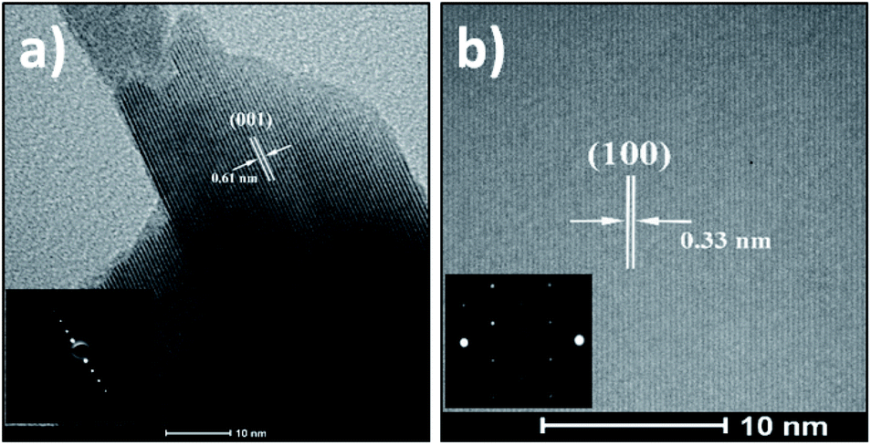 | ||
| Fig. 5 (a) TEM image of layered structures of nanosheet with the corresponding SAED pattern in inset and (b) high resolution image of the crystal showing the (001) crystal planes with in inset a SAED pattern of single nanosheet showing hexagonal spot symmetry. | ||
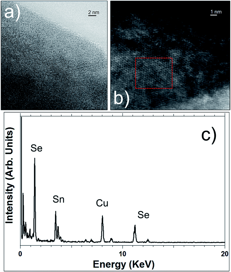 | ||
| Fig. 6 STEM images in bright-field mode (a) and in HAADF mode (b) of SnSe2 nanosheets. (c) EDS spectrum recorded in the red highlighted area of Fig. 6b. | ||
STEM imaging, bright-field and in HAADF modes (see Fig. 6), corroborates the high crystallinity of these SnSe2 nanosheets and their hexagonal structure. EDS (Fig. 6c) also confirms the SnSe2 chemical composition of those flakes and the ratio of 2 for Se/Sn.
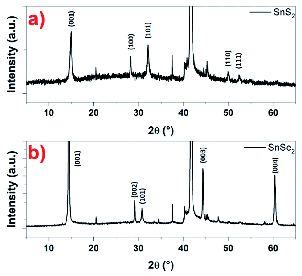
Based on the microscopy studies, the conclusions that can be drawn are that the nanosheets, whether SnS2 or SnSe2, are crystallized in a hexagonal structure. This has been checked using XRD. Indeed, in Fig. 7a, a typical XRD pattern of the as-prepared SnS2 nanosheets is shown. The diffraction peaks appearing at 14.5°, 28.6°, 32.3°, 50.2° and 52.1° are distinctly indexed to the (001), (100), (101), (110) and (111) planes of the hexagonal SnS2 phase, which are very close to the reported data (JCPDS card 23-0677) for the hexagonal 2H phase.49 In the same way, the typical XRD pattern of the so-prepared SnSe2 nanosheets in Fig. 7b show that are crystalline with a good match with the reported pattern for the hexagonal SnSe2 phase (JCPDS card 023-0602).37 Indeed, the diffraction peaks appearing at 14.5°, 29.05°, 30.7°, 44.3° and 60.3° are distinctly indexed to the (001), (002), (101), (003) and (004) planes. The peaks observed indicate the high purity and crystallinity of the products. For both samples, the intense diffraction peak around 42° corresponds to the (0001) plane of the substrate, in this case, the sapphire.
 | ||
| Fig. 7 XRD pattern recorded on: (a) SnS2 and (b) SnSe2 nanosheets, respectively. | ||
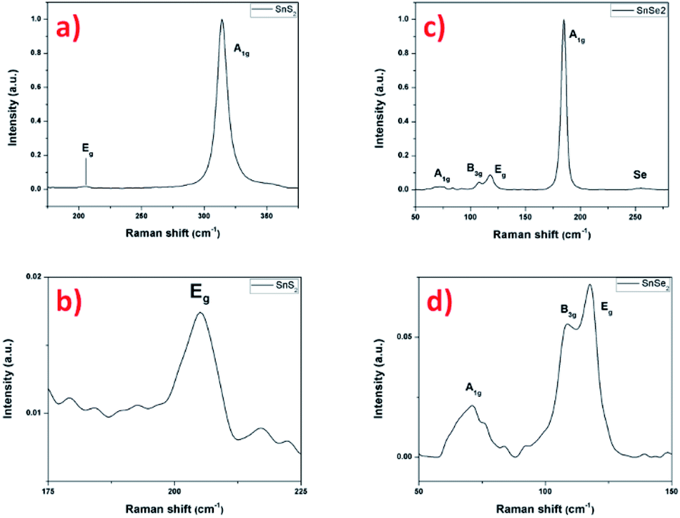
The Raman scattering measurement was done to study the signature of vibrational modes to confirm the formation of the SnS2 nanosheets. Fig. 8a shows the Raman spectrum of SnS2 nanosheets with two main peaks of 205 and 315 cm−1, assigned to the phonon modes. The most intense peak at 315 cm−1 is assigned as A1g mode corresponding to vertical out-of-plane vibration between S–S and in the Fig. 8b the Eg correspond to non-degenerate in-plane vibration mode with a single band at 205 cm−1.11,50 The low intensity of the Eg peak is explained by the low thickness of the nanosheets, reducing the in-plane scattering centers as already reported.51 The Raman signature of the SnS2 material agrees with the previous results and confirms the crystallization into hexagonal 2H structure.
 | ||
| Fig. 8 Raman spectrum with 532 nm excitation laser of SnS2 nanosheets (a and b) and SnSe2 nanosheets (c and d). | ||
In the Fig. 8c, the Raman spectrum shows an intense peak that is assigned to the A1g mode at 184 cm−1 and another very weak peak corresponding to Eg mode at 117 cm−1, signature of the SnSe2 material.52,53 The magnification of the Eg peak region surprisingly shows two small additional peaks at 70 cm−1 and 108 cm−1. These peaks cannot be definitively attributed to SnO2, as localized Raman modes on sputtered thermally oxidized tin metal were reported at different positions (typically at 112 cm−1 and 210 cm−1 for oxidation temperatures up to 400 °C with the appearance of further peaks at higher temperatures).54 Alternatively, the presence of another structure such as SnSe can be envisaged, this structure is characterized by four intense peaks in the region considered, localized at about 70, 108, 130 and 149 cm−1, related to A1g, B3g, A2g and A3g, respectively.55,56 Here, only two weak peaks are well-visible that could be attributed to the A1g and B3g modes to the SnSe material. The other two can be guesstimated in the background noise. Finally, the broad peak located at 255 cm−1 can be attributed to the presence of amorphous Se.57 This had already been reported and explained by a condensation phenomenon of Se during cooling.58
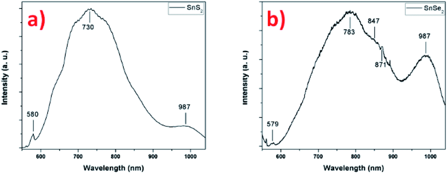
The photoluminescence of the two tin-based nanomaterials was studied at the excitation wavelength of 532 nm in Fig. 9. Fig. 9a shows the PL spectrum the SnS2 sample exhibiting different features: a low intensity peak at 580 nm (2.14 eV) that is attributed to the indirect bandgap of thin SnS2 film59,60 and a high intensity broad peak centered at 730 nm (1.70 eV) whose origin can have several sources according to the literature. Firstly, the presence of another nanomaterial, for example SnS nanosheets, giving rise to a PL emission at this energy, despite the fact that other techniques indicate the sole presence of 2H-SnS2. However, the energy does not correspond to the band gap of SnS around 825 nm (1.5 eV) and the large peak width is not characteristic of a single and well-defined energy transition.61 A report on 2D flakes of SnS2 synthesized by a wet chemical synthesis technique, shows similar features on the PL spectrum (at 532 nm) with a sharp peak at about 580 nm (indirect excitonic peak as previously assigned) and a broader peak centered at about 660 nm.11 The authors associated this transition to indirect exciton recombination of 4H phase of SnS2 present in the sample, rejecting the other possibilities due to the high quality of their synthetized SnS2 flakes (no impurities, no sulfur vacancies, etc.). In our SnS2 nanosheets, the 4H phase is not observed, what suggests another origin for this broad peak such as effect of crystalline defects/impurities or effect of interface strain between film and substrate, generating bound excitons recombination.59,62 Actually, it was reported that compared to the PL of bulk SnS2 (centered at 532 nm), the PL of exfoliated SnS2, shows a broad peak centered at 680 nm dramatically associated to electron–phonon interaction caused by the large amount of sulfur vacancies.63 Considering our SnS2 nanosheets, the structural and chemical characterizations demonstrates that high crystalline nanosheets of SnS2 have been successfully synthetized and the presence of impurities or vacancies were not observed. However, it was reported for transition metal dichalcogenide materials that bulk characterization techniques such as XRD cannot give a perfect overview of the quality of the synthesized material, which techniques such as Raman and PL spectroscopy do.64 The possibility of having vacancies/defects in the samples cannot be excluded, but due to the relative thickness of nanosheets such information is very hard to get by TEM. In addition, morphology may also influence the PL results. The nanosheets are oriented vertically with respect to the substrate, exposing their edges. Indeed, it has been shown that there is an increase in photoluminescence at the edges and also at the grain boundaries of triangular WS2 monolayers, explained by the different structure and composition of these regions compared with the center.65,66 A related study demonstrated a larger monosulfur vacancies concentration near the edges in comparison with the interior, explaining the features observed in PL.67 In agreement, in MoS2, exposed edges of the nanosheets due to the vertical orientation have been associated with enhanced PL emissions.41 To confirm this hypothesis, we performed PL experiments on a SnS2 sample with a different morphology (i.e. spheres of around 500 nm in diameter composed of small nanosheets (flower-like nanostructure, without any preferential alignment)) and compared with the result obtained on the vertically aligned SnS2 nanosheets sample (Fig. S8†). Compared to the PL spectrum recorded on the flower-like nanostructure, the PL of the vertically aligned sample is enhanced the hypothesis that the morphology plays a rule due certainly to the number of exposed edges. The conclusion we can draw from these photoluminescence experiments is that structural defects are certainly present at the edges of the nanosheets, explaining the origin and energy position of the high-intensity broader peak and the enhancement of the PL. The peak observed at 987 nm (1.26 eV) in the Fig. 9a, may be attribute to the emission signal of the substrate (Fig. S9†), in this case we used SiO2 as substrate.
 | ||
| Fig. 9 PL spectra of (a) SnS2 nanosheets and (b) SnSe2 nanosheets. | ||
Fig. 9b presents the PL spectrum of the SnSe2 sample. The first peak at 579 nm (2.15 eV) could be attributed to the direct allowed transition in SnSe2, value close to ones given in the literature.68 This value is close to one given for a monolayer and it is in agreement with the one reported for 50 nm film.69 The second broad and more intense peak located at 783 nm (1.58 eV) presents a well-defined shoulder at 847 nm (1.46 eV). For this material, few results have been reported on photoluminescence studies. However, due to the similarity of the results with the SnS2, similar conclusion could be drawn to explain the PL spectrum with the possible presence of defects/vacancies and the edges effect due to the vertical orientation of the nanosheets. A notable difference is the presence of a shoulder located at 847 cm−1 that may be associated to the presence of another phase, already detected in Raman spectroscopy. Indeed, the formation of polycrystalline thin films of SnSe and SnSe2 has been reported for low selenization temperature (<470 °C), hexagonal SnSe2 is formed and for higher temperature (<530 °C) orthorhombic SnSe become the preferential material PL.58 The authors showed for the material synthesized at 470 °C made of SnSe2, the presence of SnSe phase with a bandgap value of 1.43 eV (ref. 58) that is the close value found in our case with 1.46 eV. Surprisingly, this value does not correspond to a gap value for orthorhombic SnSe but rather to that of cubic SnSe.70 The other intense peak observed at 987 nm (1.26 eV) can be attribute, as previously shown for SnS2, to the photoluminescence emissions of the substrate. In this case, the signature of the substrate can also be found in the low intensity peak at 871 nm (1.42 eV) in the shoulder of the more intense and broader peak (see Fig. S9† for comparison). These results indicate that the SnSe2 sample is less homogeneous than SnS2 sample (as we can see in the Fig. 1) and the transitions of the substrate are more visible (Fig. S9†).
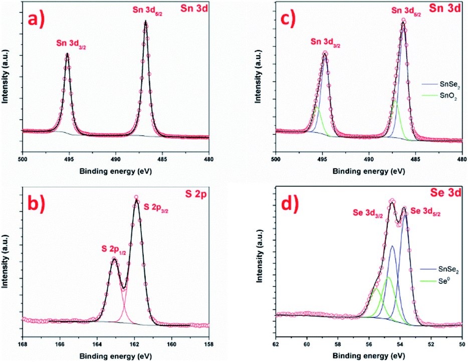
The chemistry of the as-prepared products was further investigated by XPS as shown in Fig. 10. Fig. 10a and b present the Sn 3d and S 2p core level of SnS2 samples. The Sn 3d spectrum is composed of one doublet, with contributions centered at 487.1 and 495.6 eV, attributed to Sn 3d5/2 and Sn 3d3/2 of Sn4+ in SnS2, respectively.15,71 No other contribution is observed.72 The S 2p spectrum (Fig. 10b) is composed of a one doublet, with S 2p3/2 and S 2p1/2 signal centered at 161.8 and 162.7 eV respectively, attributed to S2− species in SnS2.61 Both Sn 3d and S 2p confirms the successful formation of SnS2 phase, without another phase. The Fig. 10c and d shows Sn 3d and Se 2p signal of SnSe2 sample. The Sn 3d is composed of a first doublet, with contributions centered at 486.3 eV and 494.7 eV, attributed to Sn 3d5/2 and Sn 3d3/2 states of Sn4+ in SnSe2. A second doublet is observed, with contributions at 487.2 and 495.6 eV. The Se 3d spectrum is composed of a first doublet with contributions centered at 53.7 eV and 54.5 eV attributed to Se 3d5/2 and Se 3d3/2 of SnSe2 phase.52 Here also, a second doublet is observed, with Se 3d5/2 and Se 3d3/2 contributions centered at 54.8 eV and 55.5 eV respectively. The interpretation of selenium XPS signal is complex and the literature about XPS of SnSex reports contradictory and wrong interpretation of Se and Sn signals. One can cite the absence of Se 3d5/2 contribution in SnSe73 or an area of 3d3/2 contribution higher than the 3d5/2 in ref. 74. Here, the contribution Sn 3d at 487.2 is attributed to Sn oxide. In reference paper, SnO2 is reported at 487.8 in ref. 75, 486.8 in ref. 76 and 486.3 eV.77 The observation of Sn oxide contribution is consistent with previous results: tin oxide is formed prior to the selenization (and sulfurization), and SEM images show that some area is not covered by the nanosheet, namely the XPS also probes this surface. For SnS2, the covering is more uniform, certainly due to the total reaction of SnO2 with S. In this case, explaining that the oxidation is not observed by XPS. Concerning the second contribution in Se signal, at 54.8 eV, this contribution is not fully understood in the literature. If this contribution could be attributed to SnSe phase, in agreement with,36 one should also see a contribution in the Sn signal, at lower binding energy (shifted by ≈ −0.7 eV). The Se contribution cannot be attributed to SeO2, as this contribution is centered at much higher binding energy, around 59.5 eV.75,78 Alternatively, the formation of SnSe2−x metastable phase can be considered. Indeed, D'Olimpio et al.75 did a careful investigation of SnSe2 chemistry when exposed to different environment. However, this would imply also a contribution on the Sn signal, and this contribution would be between SnSe2 and SnSe, i.e. at a lower binding energy of 483.3 eV for the Sn 3d5/2 contribution of this metastable phase. The most probable explanation would lie in the presence of metallic selenium (Se0). The Se 3d5/2 signal of metallic selenium is reported in higher binding energies than tin selenide materials at 56.0 eV for Lee et al.79 and at 54.7 eV by Vishwanath et al.,80 this latter value is in good agreement with our data and would confirm the Raman analysis.
 | ||
| Fig. 10 XPS spectra of the SnS2 nanosheets (a) Sn 3d and (b) S 2p and SnSe2 nanosheets (c) Sn 3d and (d) Se 3d. | ||
We have demonstrated that vertically aligned nanosheets of SnS2 and SnSe2 have been synthesized using a simple and scalable method via a CVD technique using direct reaction of vapor phase (sulfur or selenium) on deposed tin films.
Discussion
With the results discussed above, a possible growth model for the SnS2 and SnSe2 aligned nanosheets prepared by using sulfurization and selenization, respectively, of pre-deposited 50 nm Sn films via magnetron sputtering is proposed. The morphologies of the tin based material produced by this method seems to be influence by different parameters, however the precursor film is the key parameter.38 Indeed, it has been shown that the magnetron sputtering parameters play an essential role in the morphologies of the deposited films, especially the argon pressure.38 By example, it has been reported that in tungsten deposit, a lower argon pressure results in a denser film structure than with a higher pressure where the film has a porous structure with cracks. The resulting tungsten selenide film results in different sheet orientations either parallel to the substrate for dense tungsten films (low argon pressure) or perpendicular to the substrate for porous films (higher argon pressure).38 Here, the film deposition has been made at 1 × 10⁻³ mbar at room temperature that is a lower value than ones reported in ref. 38 and the chemistry of the film is different, tin instead of tungsten, however the results obtained seem to follow the same trend, where the vertical alignment of the nanosheets is not observable with direct reaction (sulfurization or selenization) on the film thus prepared, certainly due to the film density. The effect of the deposition pressure on the sputtering tin films has been not studied. To overcome this problem, the solution found was to oxidize the tin film as of homogeneity is promoted. Indeed, the sputtered film is metallic but when it is transferred on air after the deposition a partial oxidation occurs due to the thickness of the film. For a homogeneous oxidation of the whole film, an oxidation step is performed. Depending on the level of oxidation, the surface will change determining the diffusion of the S/Se, which is very important for the vertically growth. Indeed, we observed that the morphology of the nanostructures strongly depends on the oxidation level before sulfurization/selenization. As an example, for sulfurization: (i) the vertical alignment of SnS2 nanosheets was not observed on tin film as sputtered (with partial oxidation in air); (ii) samples synthesized on tin film oxidized at 200 °C for 2 hours with air flow presents a flower-like morphology with short nanosheets grouped in the form of spheres without any preferential alignment; and (iii) samples synthesized on tin film oxidized at 300 °C for 2 hours with air flow shows a vertical orientation of the nanosheets with uniformly distribution in all the surface. Therefore, it can be postulated that depending on the level of oxidation, different thickness of the film will be oxidized and this will determine the diffusion of S/Se, a very important factor for vertical growth of nanosheets. Indeed, it has been reported that the diffusion of S/Se through the film is necessary and that this process is the limiting factor for the orientation of the nanosheets.40 According to our experimental data, the sulfur diffusion increases with the thickness of the oxidized layer, it seems that S interacts just with Sn near the film surface for case (ii) and short nanosheets are formed, while for case (iii) due to the higher temperature the Sn diffuses deeper leading to a pronounced change of the surface morphology. Another parameter reported in the literature playing an important role in the final product characteristics is the composition of the reactive atmosphere near the film, more or less rich in S/Se.81 Indeed, it has been shown for MoS2 that in order to have a complete reaction with the oxidized film, it is necessary to have an atmosphere rich in S for this to be the dominant mechanism, instead of having an atmosphere deficient in S, as in this case the modification of the surface occurs due to the dominant mechanism of oxide segregation/coalescence.81 The effect of the sulfur concentration during the synthesis was not evaluated, however we can assume that the atmosphere is rich enough in S/Se for the sulfurization/selenization reaction to occur. Therefore, the Sn oxide film is reduced by sulfur or selenium and we obtained SnS2 or SnSe2 in a short synthesis time. A very fast reduction of Sn oxides by S/Se might have an important role in the formation of vertically aligned layered nanosheets. The growth of nanosheets, occurs along two directions ([001] and [100]), with higher growth velocity along [001] leading to the formation of sheet-like structures. The vertical alignment of nanosheets formation is possibly favored by its anisotropic atomic bonding nature. The differences in the reactivity of sulfur and selenium plays an important role in the syntheses of the SnS2 and SnSe2 nanomaterials. Certainly, Se chemical reactivity is much lower than S one and a suitable reducer agent is required.82 For that, it is necessary the addition of H2 to promote the formation of H2Se which in turn provides atomic Se for the formation of SnSe2,58 because without H2 the growth of SnSe2 does not occur. Furthermore, the presence of hydrogen can also lead to the reduction of the oxidized tin film, which is not the goal. However, by optimizing the amount of hydrogen introduced, the selenization reaction occurs to produce vertically aligned layered SnSe2 nanosheets. We perceived that while during the synthesis of SnSe2, SnSe was formed, in the case of SnS2, the SnS was not observed. This can be explained by the thermodynamic conditions of the reaction. It has been shown that the reaction to form SnS is not spontaneous in an inert atmosphere as in our case where only argon is introduced during the reaction. If hydrogen had been used during the synthesis, the SnS material could have been synthesized as it requires a reducing atmosphere.51 Concerning the selenium material, the presence of hydrogen is necessary as described above to obtain the correct selenium reactive species, allowing the formation of the different selenium materials. A last parameter to consider is the temperature. It has been shown that temperature plays a major role in phase selection between SnSe and SnSe2,36,58 a lower selenization temperature allows the formation of a dominant SnSe2 phase, whereas a higher temperature leads to the formation of the SnSe phase (this is also dependent on other parameters such as the gases in the reaction chamber). With an intermediate temperature, a mixture of the two phases can be observed.58 Our reaction occurs at 450 °C, which is a relatively low selenization temperature in the range of temperatures reported for the synthesis of the SnSe2 phase, therefore explaining the observation of a mix of both phases, as we reported in this work. This temperature is not far from the intermediate temperature between the SnSe2 and SnSe formation temperatures, which explains the fact that domains of the other SnSe phase can be found in a product composed mainly of SnSe2. This fact have been already reported in ref. 58 for a selenization temperature of 470 °C. Finally, for such syntheses, the temperature is relatively low compared to the formation temperatures of other metal dichalcogenides, which may also explain the presence of structural defects (vacancies).Conclusions
We have demonstrated the synthesis of vertically aligned SnS2 and SnSe2 nanosheets. This was achieved using a simple one-step CVD technique by direct sulfurization/selenization of a pre-oxidized tin film. We evidenced the quality of the as-synthesized materials by employing XRD, Raman spectroscopy, XPS and electron microscopies. Vertical and homogeneous alignment of well-crystalline 2H-phase SnS2 nanosheets have been demonstrated, the nanosheets, however, having structural defects at their edges. The SnSe2 nanomaterial has the same form as the SnS2 nanomaterial, i.e. vertical alignment and well-crystalline 2H phase with also structural defects at their edges, however with some differences were observed: the nanosheets are larger, less homogeneity, presence of another nanomaterial SnSe as well as unreacted selenium. The growth mechanism is discussed on the basis of our results.Author contributions
A. S.-C. and J.-F. C. conceived, and carried out the experiments. E. H. contributed to XPS measurements and analysis. S. A. and C. B. contributed to the Raman and PL measurements. R. A. contributed to STEM and EDS measurements and analysis. A. S.-C. and J.-F. C. made the analysis of the data. A. S.-C. and J.-F. C. wrote the manuscript. All of the authors provided critical feedback and helped shape the research and analysis. All authors have read and agreed to the published version of the manuscript.Conflicts of interest
The authors declare that they have no competing interests.Acknowledgements
This research work was financed by a grant from the University of Namur. C. Bittencourt and J.-F. Colomer are Research Associates of the National Funds for Scientific Research (FRS-FNRS, Belgium). CB thanks the Belgian Fund for Scientific Research under the FRFC contract CDR J001019. The Electron Microscopy Unit, member of Morph-IM platform from the UNamur, is acknowledged for electron microscopy facilities. The SIAM (Synthesis, Irradiation and Analysis of Matter) and PC2 platforms of the UNamur are acknowledged for XPS and XRD measurements respectively. The STEM measurements were performed in the Laboratorio de Microscopias Avanzadas (LMA) at the Universidad de Zaragoza (Spain). R.A. acknowledges funding from the Spanish MICINN (project grant PID2019-104739GB-100/AEI/10.13039/501100011033), from the Government of Aragon (project DGA E13-17R (FEDER, EU)) and from the European Union H2020 programs “ESTEEM3” (grant number 823717) and “Graphene Flagship – CORE3” (grant number 881603).Notes and references
- Y. H. Lee, X. Q. Zhang, W. Zhang, M. T. Chang, C. Te Lin, K. Di Chang, Y. C. Yu, J. T. W. Wang, C. S. Chang, L. J. Li and T. W. Lin, Adv. Mater., 2012, 24, 2320–2325 CrossRef CAS PubMed.
- A. L. Elías, N. Perea-López, A. Castro-Beltrán, A. Berkdemir, R. Lv, S. Feng, A. D. Long, T. Hayashi, Y. A. Kim, M. Endo, H. R. Gutiérrez, N. R. Pradhan, L. Balicas, T. E. Mallouk, F. López-Urías, H. Terrones and M. Terrones, ACS Nano, 2013, 7, 5235–5242 CrossRef PubMed.
- D. Kong, H. Wang, J. J. Cha, M. Pasta, K. J. Koski, J. Yao and Y. Cui, Nano Lett., 2013, 13, 1341–1347 CrossRef CAS PubMed.
- J.-K. Huang, P. Jiang, C.-L. Hsu, M.-H. Chiu, Z.-Y. Juang, Y.-H. Chang, W.-H. Chang, Y. Iwasa, T. Takenobu and L.-J. Li, ACS Nano, 2014, 8, 923–930 CrossRef CAS PubMed.
- X. Zhou, Q. Zhang, L. Gan, H. Li and T. Zhai, Adv. Funct. Mater., 2016, 26, 4405–4413 CrossRef CAS.
- L. Huang, Y. Yu, C. Li and L. Cao, J. Phys. Chem. C, 2013, 117, 6469–6475 CrossRef CAS.
- D. Sarkar, W. Liu, X. Xie, A. C. Anselmo, S. Mitragotri and K. Banerjee, ACS Nano, 2014, 8, 3992–4003 CrossRef CAS PubMed.
- X. Wang, P. Wang, J. Wang, W. Hu, X. Zhou, N. Guo, H. Huang, S. Sun, H. Shen, T. Lin, M. Tang, L. Liao, A. Jiang, J. Sun, X. Meng, X. Chen, W. Lu and J. Chu, Adv. Mater., 2015, 27, 6575–6581 CrossRef CAS PubMed.
- A. Jäger-Waldau, M. C. Lux-Steiner and E. Bucher, Solid State Phenom., 1994, 37–38, 479–484 Search PubMed.
- M. L. Tsai, S. H. Su, J. K. Chang, D. S. Tsai, C. H. Chen, C. I. Wu, L. J. Li, L. J. Chen and J. H. He, ACS Nano, 2014, 8, 8317–8322 CrossRef CAS PubMed.
- J. Z. Ou, W. Ge, B. Carey, T. Daeneke, A. Rotbart, W. Shan, Y. Wang, Z. Fu, A. F. Chrimes, W. Wlodarski, S. P. Russo, Y. X. Li and K. Kalantar-Zadeh, ACS Nano, 2015, 9, 10313–10323 CrossRef CAS PubMed.
- L. D. Bharatula, M. B. Erande, I. S. Mulla, C. S. Rout and D. J. Late, RSC Adv., 2016, 6, 105421–105427 RSC.
- E. Lifshitz, Z. Chen and L. Bykov, J. Phys. Chem., 1993, 97, 238–242 CrossRef CAS.
- S. Mandalidis, J. A. Kalomiros, K. Kambas and A. N. Anagnostopoulos, J. Mater. Sci., 1996, 31, 5975–5978 CrossRef CAS.
- W. Sun, X. Rui, D. Yang, Z. Sun, B. Li, W. Zhang, Y. Zong, S. Madhavi, S. Dou and Q. Yan, ACS Nano, 2015, 9, 11371–11381 CrossRef CAS PubMed.
- M. Chen, Z. Li, W. Li, C. Shan, W. Li, K. Li, G. Gu, F. Ye, G. Zhong and L. Wei, Nanotech, 2018, 29, 455501 CrossRef PubMed.
- Y. Sun, H. Cheng, S. Gao, Z. Sun, Q. Liu, Q. Leu, F. Lei, T. Yao, J. He, S. Wei and Y. Xie, Angew. Chem., Int. Ed., 2012, 51, 8727–8731 CrossRef CAS PubMed.
- Y. Huang, E. Sutter, J. T. Sadowski, M. Cotlet, O. L. A. Monti, D. A. Racke, M. R. Neupane, D. Wickramaratne, R. K. Lake, B. A. Parkinson and P. Sutter, ACS Nano, 2014, 8, 10743–10755 CrossRef CAS PubMed.
- B. Thangaraju and P. Kaliannan, J. Phys. D: Appl. Phys., 2000, 33, 1054–1059 CrossRef CAS.
- R. W. Miles, O. E. Ogah, G. Zoppi and I. Forbes, Thin Solid Films, 2009, 517, 4702–4705 CrossRef CAS.
- J. J. Wu, Y. R. Tao, X. C. Wu and Y. Chun, J. Alloys Compd., 2017, 713, 38–45 CrossRef CAS.
- Y. Tao, X. Wu, W. Wang and J. Wang, J. Mater. Chem. C, 2015, 3, 1347–1353 RSC.
- G. Ye, Y. Gong, S. Lei, Y. He, B. Li, X. Zhang, Z. Jin, L. Dong, J. Lou, R. Vajtai, W. Zhou and P. M. Ajayan, Nano Res., 2017, 10, 2386–2394 CrossRef CAS.
- H. S. Song, S. L. Li, L. Gao, Y. Xu, K. Ueno, J. Tang, Y. B. Cheng and K. Tsukagoshi, Nanoscale, 2013, 5, 9666–9670 RSC.
- G. Deokar, D. Vignaud, R. Arenal, P. Louette and J. Colomer, Nanotechnology, 2016, 27, 075604 CrossRef CAS PubMed.
- A. Sierra-Castillo, E. Haye, S. Acosta, C. Bittencourt and J. F. Colomer, Appl. Sci., 2020, 10, 874 CrossRef CAS.
- S. Y. Cho, S. J. Kim, Y. Lee, J. S. Kim, W. Bin Jung, H. W. Yoo, J. Kim and H. T. Jung, ACS Nano, 2015, 9, 9314–9321 CrossRef PubMed.
- G. Deokar, N. S. Rajput, J. Li, F. L. Deepak, W. Ou-Yang, N. Reckinger, C. Bittencourt, J. F. Colomer and M. Jouiad, Beilstein J. Nanotechnol., 2018, 9, 1686–1694 CrossRef CAS PubMed.
- C. Backes, A. M. Abdelkader, C. Alonso, A. Andrieux-Ledier, R. Arenal, J. Azpeitia, N. Balakrishnan, L. Banszerus, J. Barjon, R. Bartali, S. Bellani, C. Berger, R. Berger, M. M. B. Ortega, C. Bernard, P. H. Beton, A. Beyer, A. Bianco, P. Bøggild, F. Bonaccorso, G. B. Barin, C. Botas, R. A. Bueno, D. Carriazo, A. Castellanos-Gomez, M. Christian, A. Ciesielski, T. Ciuk, M. T. Cole, J. Coleman, C. Coletti, L. Crema, H. Cun, D. Dasler, D. De Fazio, N. Díez, S. Drieschner, G. S. Duesberg, R. Fasel, X. Feng, A. Fina, S. Forti, C. Galiotis, G. Garberoglio, J. M. García, J. A. Garrido, M. Gibertini, A. Gölzhäuser, J. Gómez, T. Greber, F. Hauke, A. Hemmi, I. Hernandez-Rodriguez, A. Hirsch, S. A. Hodge, Y. Huttel, P. U. Jepsen, I. Jimenez, U. Kaiser, T. Kaplas, H. K. Kim, A. Kis, K. Papagelis, K. Kostarelos, A. Krajewska, K. Lee, C. Li, H. Lipsanen, A. Liscio, M. R. Lohe, A. Loiseau, L. Lombardi, M. F. López, O. Martin, C. Martín, L. Martínez, J. A. Martin-Gago, J. I. Martínez, N. Marzari, Á. Mayoral, J. McManus, M. Melucci, J. Méndez, C. Merino, P. Merino, A. P. Meyer, E. Miniussi, V. Miseikis, N. Mishra, V. Morandi, C. Munuera, R. Muñoz, H. Nolan, L. Ortolani, A. K. Ott, I. Palacio, V. Palermo, J. Parthenios, I. Pasternak, A. Patane, M. Prato, H. Prevost, V. Prudkovskiy, N. Pugno, T. Rojo, A. Rossi, P. Ruffieux, P. Samorì, L. Schué, E. Setijadi, T. Seyller, G. Speranza, C. Stampfer, I. Stenger, W. Strupinski, Y. Svirko, S. Taioli, K. B. K. Teo, M. Testi, F. Tomarchio, M. Tortello, E. Treossi, A. Turchanin, E. Vazquez, E. Villaro, P. R. Whelan, Z. Xia, R. Yakimova, S. Yang, G. R. Yazdi, C. Yim, D. Yoon, X. Zhang, X. Zhuang, L. Colombo, A. C. Ferrari and M. Garcia-Hernandez, 2D Mater., 2020, 7, 022001 CrossRef CAS.
- Y. Fu, G. Gou, X. Wang, Y. Chen, Q. Wan, J. Sun, S. Xiao, H. Huang, J. Yang and G. Dai, Appl. Phys. A: Mater. Sci. Process., 2017, 123, 1–8 CrossRef CAS.
- J. Xia, D. Zhu, L. Wang, B. Huang, X. Huang and X. M. Meng, Adv. Funct. Mater., 2015, 25, 4255–4261 CrossRef CAS.
- G. Liu, Z. Li, T. Hasan, X. Chen, W. Zheng, W. Feng, D. Jia, Y. Zhou and P. A. Hu, J. Mater. Chem. A, 2017, 5, 1989–1995 RSC.
- X. Zhou, L. Gan, W. Tian, Q. Zhang, S. Jin, H. Li, Y. Bando, D. Golberg and T. Zhai, Adv. Mater., 2015, 27, 8035–8041 CrossRef CAS PubMed.
- B. An, Y. Ma, G. Zhang, C. You and Y. Zhang, RSC Adv., 2020, 10, 42157–42163 RSC.
- J. Wu, Z. Hu, Z. Jin, S. Lei, H. Guo, K. Chatterjee, J. Zhang, Y. Yang, B. Li, Y. Liu, J. Lai, R. Vajtai, B. Yakobson, M. Tang, J. Lou and P. M. Ajayan, Adv. Mater. Interfaces, 2016, 3, 1–8 CAS.
- D. Lu, C. Yue, S. Luo, Z. Li, W. Xue, X. Qi and J. Zhong, Appl. Surf. Sci., 2021, 541, 148615 CrossRef CAS.
- N. D. Boscher, C. J. Carmalt, R. G. Palgrave and I. P. Parkin, Thin Solid Films, 2008, 516, 4750–4757 CrossRef CAS.
- H. Li, D. Gao, K. Li, M. Pang, S. Xie, R. Liu and J. Zou, Appl. Surf. Sci., 2017, 394, 142–148 CrossRef CAS.
- H. Li, H. Wu, S. Yuan and H. Qian, Sci. Rep., 2016, 6, 1–9 CrossRef PubMed.
- D. Kong, H. Wang, J. J. Cha, M. Pasta, K. J. Koski, J. Yao and Y. Cui, Nano Lett., 2013, 13, 1341–1347 CrossRef CAS PubMed.
- G. Deokar, N. S. Rajput, P. Vancsó, F. Ravaux, M. Jouiad, D. Vignaud, F. Cecchet and J. F. Colomer, Nanoscale, 2017, 9, 277–287 RSC.
- M. R. Linford, V. S. Smentkowski, J. T. Grant, C. R. Brundle, P. M. A. Sherwood, M. C. Biesinger, J. Terry, K. Artyushkova, A. Herrera-Gómez, S. Tougaard, W. Skinner, J. J. Pireaux, C. F. McConville, C. D. Easton, T. R. Gengenbach, G. H. Major, P. Dietrich, A. Thissen, M. Engelhard, C. J. Powell, K. J. Gaskell and D. R. Baer, Microsc. Microanal., 2019, 1–2 Search PubMed.
- V. J. Inglezakis, A. Satayeva, A. Yagofarova, Z. Tauanov, K. Meiramkulova, J. Farrando-Pérez and J. C. Bear, Nanomaterials, 2020, 10, 1156 CrossRef CAS PubMed.
- G. Greczynski and L. Hultman, Prog. Mater. Sci., 2020, 107, 100591 CrossRef CAS.
- J.-G. Wang, H. Sun, H. Liu, D. Jin, R. Zhou and B. Wei, J. Mater. Chem. A, 2017, 5, 23115–23122 RSC.
- J. Huang, Y. Deng, H. X. Xu, K. Wang, Z. X. Wang, Q. S. Wang and F. M. He, Nanoscale, 2015, 7, 14093–14099 RSC.
- S. Saha, A. Banik and K. Biswas, Chem.–Eur. J., 2016, 22, 15634–15638 CrossRef CAS PubMed.
- Y. Huang, K. Xu, Z. Wang, T. A. Shifa, Q. Wang, F. Wang, C. Jiang and J. He, Nanoscale, 2015, 7, 17375–17380 RSC.
- Y. Jiang, Y. Feng, B. Xi, S. Kai, K. Mi, J. Feng, J. Zhang and S. Xiong, J. Mater. Chem. A, 2016, 4, 10719–10726 RSC.
- C. S. Rout, P. D. Joshi, R. V. Kashid, D. S. Joag, M. A. More, A. J. Simbeck, M. Washington, S. K. Nayak and D. J. Late, Appl. Phys. Lett., 2014, 105, 043109 CrossRef.
- J. H. Ahn, M. J. Lee, H. Heo, J. H. Sung, K. Kim, H. Hwang and M. H. Jo, Nano Lett., 2015, 15, 3703–3708 CrossRef CAS PubMed.
- Y. Zhang, Y. Shi, M. Wu, K. Zhang, B. Man and M. Liu, Nanomaterials, 2018, 8, 515 CrossRef PubMed.
- R. K. Rai, S. Islam, A. Roy, G. Agrawal, A. K. Singh, A. Ghosh and N. Ravishankar, Nanoscale, 2019, 11, 870–877 RSC.
- D. M. Jang, H. Jung, N. D. Hoa, D. Kim, S. K. Hong and H. Kim, J. Nanosci. Nanotechnol., 2012, 12, 1425–1428 CrossRef CAS PubMed.
- X. Xu, Q. Song, H. Wang, P. Li, K. Zhang, Y. Wang, K. Yuan, Z. Yang, Y. Ye and L. Dai, ACS Appl. Mater. Interfaces, 2017, 9, 12601–12607 CrossRef CAS PubMed.
- S. Luo, X. Qi, H. Yao, X. Ren, Q. Chen and J. Zhong, J. Phys. Chem. C, 2017, 121, 4674–4679 CrossRef CAS.
- V. S. Minaev, S. P. Timoshenkov and V. V. Kalugin, J. Optoelectron. Adv. Mater., 2005, 7, 1717–1741 CAS.
- P. A. Fernandes, M. G. Sousa, P. M. P. Salomé, J. P. Leitão and A. F. Da Cunha, CrystEngComm, 2013, 15, 10278–10286 RSC.
- N. G. Deshpande, A. A. Sagade, Y. G. Gudage, C. D. Lokhande and R. Sharma, J. Alloys Compd., 2007, 436, 421–426 CrossRef CAS.
- J. George and K. S. Joseph, J. Phys. D: Appl. Phys., 1982, 15, 1109–1116 CrossRef CAS.
- M. Cao, K. Yao, C. Wu, J. Huang, W. Yang, L. Zhang, F. Lei, Y. Sun, L. Wang and Y. Shen, ACS Appl. Energy Mater., 2018, 1, 6497–6504 CrossRef.
- G. Ham, S. Shin, J. Park, J. Lee, H. Choi, S. Lee and H. Jeon, RSC Adv., 2016, 6, 54069–54075 RSC.
- Z. Qin, K. Xu, H. Yue, H. Wang, J. Zhang, C. Ouyang, C. Xie and D. Zeng, Sens. Actuators, B, 2018, 262, 771–779 CrossRef CAS.
- A. McCreary, A. Berkdemir, J. Wang, M. A. Nguyen, A. L. Elías, N. Perea-López, K. Fujisawa, B. Kabius, V. Carozo, D. A. Cullen, T. E. Mallouk, J. Zhu and M. Terrones, J. Mater. Res., 2016, 31, 931–944 CrossRef CAS.
- H. R. Gutiérrez, N. Perea-López, A. L. Elías, A. Berkdemir, B. Wang, R. Lv, F. López-Urías, V. H. Crespi, H. Terrones and M. Terrones, Nano Lett., 2013, 13, 3447–3454 CrossRef PubMed.
- M. S. Kim, S. J. Yun, Y. Lee, C. Seo, G. H. Han, K. K. Kim, Y. H. Lee and J. Kim, ACS Nano, 2016, 10, 2399–2405 CrossRef CAS PubMed.
- V. Carozo, Y. Wang, K. Fujisawa, B. R. Carvalho, A. McCreary, S. Feng, Z. Lin, C. Zhou, N. Perea-López, A. L. Elías, B. Kabius, V. H. Crespi and M. Terrones, Sci. Adv., 2017, 3, 1–10 Search PubMed.
- M. M. El-Nahass, J. Mater. Sci., 1992, 27, 6597–6604 CrossRef CAS.
- E. P. Mukhokosi, S. B. Krupanidhi and K. K. Nanda, Sci. Rep., 2017, 7, 1–10 CrossRef CAS PubMed.
- P. K. Nair, E. Barrios-Salgado and M. T. S. Nair, Phys. Status Solidi A, 2016, 213, 2229–2236 CrossRef CAS.
- Y. Jiang, M. Wei, J. Feng, Y. Ma and S. Xiong, Energy Environ. Sci., 2016, 9, 1430–1438 RSC.
- C. Zhai, N. Du, H. Zhang, J. Yu and D. Yang, ACS Appl. Mater. Interfaces, 2011, 3, 4067–4074 CrossRef CAS PubMed.
- T. Yan, Y. Han, Q. Fu, T. Xu, S. Yin, W. Wu and W. Liu, Opt. Mater., 2020, 108, 110440 CrossRef CAS.
- M. Pawar, S. Kadam and D. J. Late, ChemistrySelect, 2017, 2, 4068–4075 CrossRef CAS.
- G. D'Olimpio, F. Genuzio, T. O. Menteş, V. Paolucci, C. N. Kuo, A. Al Taleb, C. S. Lue, P. Torelli, D. Fariás, A. Locatelli, D. W. Boukhvalov, C. Cantalini and A. Politano, J. Phys. Chem. Lett., 2020, 9003–9011 CrossRef PubMed.
- D. Barreca, S. Garon, E. Tondello and P. Zanella, Surf. Sci. Spectra, 2000, 7, 81–85 CrossRef CAS.
- M. A. Stranick and A. Moskwa, Surf. Sci. Spectra, 1993, 2, 50–54 CrossRef CAS.
- Y. Fan, Y. Zhuo and L. Li, Appl. Surf. Sci., 2017, 420, 465–471 CrossRef CAS.
- L. Lee, C. W. Chen, A. Manikandan, S. H. Lee, Z. M. Wang and Y. L. Chueh, Nano Energy, 2018, 44, 419–429 CrossRef.
- S. Vishwanath, X. Liu, S. Rouvimov, L. Basile, N. Lu, A. Azcatl, K. Magno, R. M. Wallace, M. Kim, J. C. Idrobo, J. K. Furdyna, D. Jena and H. G. Xing, J. Mater. Res., 2016, 31, 900–910 CrossRef CAS.
- C. R. Wu, X. R. Chang, C. H. Wu and S. Y. Lin, Sci. Rep., 2017, 7, 1–8 CrossRef PubMed.
- J.-K. Huang, P. Jiang, C.-L. Hsu, M.-H. Chiu, Z.-Y. Juang, Y.-H. Chang, W.-H. Chang, Y. Iwasa, T. Takenobu and L. J. Li, ACS Nano, 2014, 8, 923–930 CrossRef CAS PubMed.
Footnote |
| † Electronic supplementary information (ESI) available. See DOI: 10.1039/d1ra05672g |
| This journal is © The Royal Society of Chemistry 2021 |