
 Open Access Article
 This Open Access Article is licensed under a Creative Commons Attribution-Non Commercial 3.0 Unported Licence
Electronic and optical properties of two-dimensional heterostructures based on Janus XSSe (X = Mo, W) and Mg(OH)2: a first principles investigation
Junbin Loua,
Kai Ren *b,
Zhaoming Huang*c,
Wenyi Huob,
Zhengyang Zhuc and
Jin Yud
*b,
Zhaoming Huang*c,
Wenyi Huob,
Zhengyang Zhuc and
Jin Yud
aSchool of Information Science and Engineering, Jiaxing University, Jiaxing, Zhejiang, China
bSchool of Mechanical and Electronic Engineering, Nanjing Forestry University, Nanjing, Jiangsu, China. E-mail: kairen@njfu.edu.cn
cSchool of Mechanical Engineering, Wanjiang University of Technology, Maanshan, Anhui, China
dSchool of Materials Science and Engineering, Southeast University, Nanjing, Jiangsu, China
First published on 2nd September 2021
Abstract
Two-dimensional (2D) materials have attracted numerous investigations after the discovery of graphene. 2D van der Waals (vdW) heterostructures are a new generation of layered materials, which can provide more desirable applications. In this study, the first principles calculation was implemented to study the heterostructures based on Janus TMDs (MoSSe and WSSe) and Mg(OH)2 monolayers, which were constructed by vdW interactions. Both MoSSe/Mg(OH)2 and WSSe/Mg(OH)2 vdW heterostructures have thermal and dynamic stability. Besides, XSSe/Mg(OH)2 (X = Mo, W) possesses a direct bandgap with a type-I band alignment, which provides promising applications for light-emitting devices. The charge density difference was investigated, and 0.003 (or 0.0042) |e| were transferred from MoSSe (or WSSe) layer to Mg(OH)2 layer, and the potential drops were calculated to be 11.59 and 11.44 eV across the interface of the MoSSe/Mg(OH)2 and WSSe/Mg(OH)2 vdW heterostructures, respectively. Furthermore, the MoSSe/Mg(OH)2 and WSSe/Mg(OH)2 vdW heterostructures have excellent optical absorption wave. Our studies exhibit an effective method to construct new heterostructures based on Janus TMDs and develop their applications for future light emitting devices.
1. Introduction
Nowadays, two-dimensional (2D) materials have attracted numerous investigations since graphene was prepared by a mechanical stripping method.1 Graphene was discovered to have novel thermal and electronic properties resulting from the linear band structure near the Dirac cone with zero bandgap.2–9 However, these characteristics of graphene also limit the applications in some nano-devices, which ueged the studies on 2D semiconductors.10–17 Transition metal dichalcogenide (TMD) materials are one of the common layered semiconductor materials, which have excellent electronic,18 thermal,19 and optical properties.20,21 For example, the n-doping of WSe2 was performed by the chemical vapor deposition (CVD) method, which can be used as an air-stable n-MOSFET possessing a mobility of about 70 cm2 V−1 s−1.22 MoS2 has high interfacial thermal conductance, about 2.0 × 10⁸ W K−1 m−2 with Au by different interfacial angles, and the thermal ability of TMDs can also be decided by layers.23 Similar to graphene nanoribbons, the mobility of the MoS2 monolayer is 200 cm2 V−1 s−1 at room temperature, indicating promising applications in tunnel FETs and transistors.24 TMD materials are also reported to act as substrates to prepare 2D germanene25 or nitrogen-doped graphene, which are efficient catalysts for redox reactions.26 All these excellent properties of 2D materials show the promising applications for further nano-devices.27–31In order to expand the application of these layered materials, more interesting properties were developed by the prediction of 2D materials.32–36 For example, δ-phosphorene was proposed to be an auxetic material with a high negative Poisson's ratio (NPR) of about −0.267 along relative direction.37 FeB2 monolayer possesses a Dirac cone, which endows it with a Fermi velocity larger than that of graphene.38 Using first principles calculations, 2D TiC3 was reported by a remarkably novel storage capacity of about 1278 mA h g−1 even with low barrier energy.39 The new generation of 2D materials are promising candidates for the usages of photocatalytic, photovoltaic, and optical devices.40 Besides, constructing a heterostructure by two different layered materials is also a decent method to create more applications for 2D materials.41–43 The novel electronic,44 interfacial45 and optical29 properties of heterostructures formed by van der Waals (vdW) interactions have been exploited for catalysis,46,47 electronics and optoelectronics.48 C2N/WS2 vdW possesses a high carrier mobility of 2406.50 cm2 V−1 s−1 for holes along some transportation directions.49 BCN/C2N vdW can be used as a direct Z-Scheme photocatalyst for water splitting with the e–h recombination time of about 2 ps.50 Recently, black/red phosphorus was investigated to possess type-I band alignment and also could switch to a Z-scheme photocatalyst.51 A type-I heterostructure, MoTe2/WSe2, showed a novel photoluminescence performance from the MoTe2 layer (about 1.1 eV).52 The PbI2/WS2 heterostructure also possessed an intrinsic type-I band structure with a decent narrower bandgap; interestingly, the diffusion coefficients of PbI2 for electrons and holes were similar to about 0.039 and 0.032 cm2 s−1, respectively.53 All these studies demonstrate the promising applications for future light emitting devices54 and optoelectronic applications.55–57 Recently, among tremendous 2D material family, TMDs with the Janus structure have attracted wide attention, which destroy the symmetry of the original crystal structure inducing more novel properties10,58 after the preparation of MoSSe.59,60 The Janus TMD materials have pronounced carrier mobility ranging from 28 to 606 cm2 V−1 s−1.61,62 Besides, a Janus chromium dichalcogenide was proved to have the ability to separate the photogenerated electrons and holes, and the excited carriers had a lifetime of about 2 ns calculated by the time domain density functional theory.63 Interestingly, the electronic property of the MoSSe monolayer can be tuned by a tensile strain from direct to indirect bandgap, and the excellent visible-light absorption performance promises its use as a photocatalyst.64 The WSSe monolayer can be used as a promising HER catalyst because the basal plane can be easily activated and such Janus asymmetry can enhance the HER activity.65 The dipole moment, vibrational frequency, and Rashba parameters of WSSe were also induced by its asymmetric Janus structure,66 which have potential usage for efficient photocatalysts. More recently, monolayered Mg(OH)2 sheets were reported to be obtained by the hydrothermal crystal growth technique with stable and classy chemical and vibrational properties, which are potential candidates as flexible optoelectronics.67 2D Mg(OH)2 also showed unique structural and electronic characteristics in the heterostructure.68,69 Moreover, some MoSSe- and WSSe-based heterostructures have been reported, such as MoSSe/WSSe,70 Hf2NT2/MSSe (T = F, O, OH; M = Mo, W),71 MoSSe/WSe2,72 graphene/MoSSe,73 while reports on MoSSe/Mg(OH)2 and WSSe/Mg(OH)2 heterostructures are still rare. Therefore, considering such novel electronic and optical properties of such synthesized MoSSe, WSSe and Mg(OH)2, it is worth constructing the heterostructures by XSSe (X = Mo, W) and Mg(OH)2 to develop the charming characteristics and the potential applications.
Therefore, in this study, we performed the first principles calculation, to investigate the heterostructures formed by Janus TMDs (MoSSe and WSSe) and Mg(OH)2. After deciding the structure of the heterostructures, the thermal and dynamic stabilities were addressed. Then, the band alignment of those layered materials was checked, and the interfacial characteristics, charge density difference and potential drop were studied. The optical properties were also calculated from the optical absorption spectrum.
2. Methods
Based on the density functional theory (DFT), in this simulation work, the first principles calculation was employed, which was implemented by the Vienna ab initio simulation package (VASP).74 We used the projector augmented wave potentials (PAW) and generalized gradient approximation (GGA) to explain the core electron and exchange correlation functional, respectively,75–77 using the Perdew–Burke–Ernzerhof (PBE) functional. To achieve more accurate results of the bandgap, the Heyd–Scuseria–Ernzerhof (HSE06; screening parameter 0.2 Å−1, mixing parameter 0.25) exchange–correlation functionals were used.78 The cut-off energy was set as 550 eV, and the k-point grids of the Monkhorste–Pack in the first Brillouin zone was 15 × 15 × 1. Besides, the DFT-D3 method of Grimme was also conducted for the corrections of the vdW and dipole.79 A thickness of 25 Å was employed for the vacuum layer to prevent the interactions of the layers. The energy of the calculated system and Hellmanne–Feynman force were controlled with a convergence within 1 × 10⁻⁵ eV and 0.01 eV·Å−1, respectively. For the calculation of the phonon spectra, the density functional perturbation theory (DFPT) within the PHONOPY code was used.80,81The binding energy (E) of the layered materials in this work was calculated by the following equation:
| E = EH − EXSSe − EMg(OH)2, | (1) |
| Δρ = ρH − ρXSSe − ρMg(OH)2, | (2) |
 | (3) |
3. Results and discussion
The structures of the monolayered MoSSe, WSSe and Mg(OH)2 were optimized first, as shown in Fig. 1. The calculated lattice parameters of MoSSe, WSSe and Mg(OH)2 were 3.228, 3.269 and 3.140 Å, respectively, showing the very small lattice mismatch (about 2.76% and 4.02%) for the MoSSe/Mg(OH)2 and WSSe/Mg(OH)2 heterostructures. Besides, the bond length of Mo–S, Mo–Se, W–S, W–Se in the optimized monolayered MoSSe and WSSe were obtained as 2.414, 2.529, 2.428 and 2.542 Å, respectively. Furthermore, the band structures of those layered materials are also demonstrated in Fig. 1. It can be found that MoSSe, WSSe and Mg(OH)2 had direct bandgaps of 2.100, 2.077 and 4.690 eV, respectively, which were in good agreement with other reports.69,82 | ||
| Fig. 1 Schematic of the structures of pristine (a) MoSSe, (c) WSSe and (e) Mg(OH)2 monolayers; the blue, cyan, yellow, grey, orange, red and white spheres represent Mo, Se, S, W, Mg, O and H atoms, respectively. The band structure of pristine (b) MoSSe, (d) WSSe and (f) Mg(OH)2 monolayers obtained by the HSE06 method; the Fermi level is set as 0 shown by dash line. | ||
When the heterostructure is formed by XSSe and Mg(OH)2, 12 representative stacking structures should be taken into consideration. Fig. 2 shows these 12 different stacking configurations of XSSe/Mg(OH)2. The most stable stacking style of the XSSe/Mg(OH)2 heterostructure was decided using the binding energy (E), and the E of the XSSe/Mg(OH)2 heterostructure is explained in Table 1, which shows that S-6 is the most stable configuration with the E values of −79.752 and −81.652 meV Å−2, respectively. The calculated binding energy of XSSe/Mg(OH)2 demonstrated the vdW forces between the interface of the MoSSe (or WSSe) and Mg(OH)2 monolayers.83,84 The obtained bond length of Mo–S, Mo–Se, W–S and W–Se of MoSSe and WSSe in their heterostructures, displayed in Table 1, suggested a slight change compared to the pristine MoSSe and WSSe monolayers, which can further prove the weak vdW forces in the XSSe/Mg(OH)2 heterostructure. Besides, the distance of the interface of the MoSSe/Mg(OH)2 and WSSe/Mg(OH)2 vdW heterostructures were obtained to be 2.20 and 2.19 Å, respectively, which were also smaller than that of graphite (3.336 Å).83 Furthermore, the following investigations of the XSSe/Mg(OH)2 vdW heterostructures are all based on the S-6 stacking configuration.
 | ||
| Fig. 2 Top and side views of the XSSe/Mg(OH)2 heterostructures (X = Mo, W) constructed as different stacking styles: (a) S-1, (b) S-2, (c) S-3, (d) S-4, (e) S-5, (f) S-6, (g) S-7, (h) S-8, (i) S-9, (j) S-10, (k) S-11 and (l) S-12. | ||
| MoSSe/Mg(OH)2 | WSSe/Mg(OH)2 | |||||||||
|---|---|---|---|---|---|---|---|---|---|---|
| E | h | LMo–S | LMo–Se | LMg–O | E | h | LW–S | LW–Se | LMg–O | |
| S-1 | −76.610 | 2.54 | 2.41 | 2.53 | 2.12 | −78.157 | 2.55 | 2.42 | 2.53 | 2.13 |
| S-2 | −79.617 | 2.21 | 2.41 | 2.53 | 2.12 | −81.506 | 2.19 | 2.42 | 2.54 | 2.12 |
| S-3 | −79.719 | 2.22 | 2.41 | 2.53 | 2.12 | −81.640 | 2.19 | 2.42 | 2.53 | 2.13 |
| S-4 | −79.628 | 2.22 | 2.41 | 2.53 | 2.13 | −81.494 | 2.19 | 2.42 | 2.53 | 2.12 |
| S-5 | −76.588 | 2.55 | 2.41 | 2.53 | 2.12 | −78.124 | 2.56 | 2.42 | 2.53 | 2.13 |
| S-6 | −79.752 | 2.20 | 2.41 | 2.53 | 2.12 | −81.652 | 2.19 | 2.42 | 2.54 | 2.12 |
| S-7 | −75.259 | 2.47 | 2.41 | 2.53 | 2.12 | −57.472 | 2.15 | 2.63 | 2.62 | 2.07 |
| S-8 | −77.134 | 2.25 | 2.41 | 2.53 | 2.12 | −79.157 | 2.17 | 2.42 | 2.54 | 2.13 |
| S-9 | −77.635 | 2.21 | 2.41 | 2.53 | 2.13 | −79.517 | 2.20 | 2.42 | 2.54 | 2.13 |
| S-10 | −77.500 | 2.18 | 2.41 | 2.53 | 2.13 | −79.393 | 2.17 | 2.42 | 2.54 | 2.13 |
| S-11 | −75.248 | 2.49 | 2.41 | 2.53 | 2.13 | −76.910 | 2.48 | 2.42 | 2.54 | 2.13 |
| S-12 | −77.410 | 2.21 | 2.41 | 2.53 | 2.12 | −79.281 | 2.24 | 2.42 | 2.54 | 2.13 |
Then, we also used the AIMD method to further investigate the thermal stability of the XSSe/Mg(OH)2 vdW heterostructures with a Nosé–Hoover heat bath scheme.85 To consider the constraints of lattice translational, we constructed a 6 × 6 × 1 supercell for the MoSSe/Mg(OH)2 and WSSe/Mg(OH)2 vdW heterostructures in the AIMD simulation, which contained 288 atoms totally. The ambient temperature of the simulation was set as 300 K, and the structures of the MoSSe/Mg(OH)2 and WSSe/Mg(OH)2 vdW heterostructures after relaxation for 5 ps are shown in Fig. 3(a) and (d), respectively. It can be found that the structures of the MoSSe/Mg(OH)2 and WSSe/Mg(OH)2 vdW heterostructures still remained intact after 5 ps under 300 K, revealing the robust thermal stability of the heterostructures. In addition, the change of temperature and total energy during the AIMD calculation of both layered systems are shown in Fig. 3(b) and (e), respectively. The temperature and total energy exhibited a convergence with the simulation step, guaranteeing the reliability of the results. The phonon dispersions were calculated (Fig. 3(c) and (d)) to further evaluate the stability of the MoSSe/Mg(OH)2 and WSSe/Mg(OH)2 vdW heterostructures. It is worth noting that no imaginary frequency existed in their phonon spectra, suggesting a dynamic stability.
 | ||
| Fig. 3 The snapshot of the (a) MoSSe/Mg(OH)2 and (d) WSSe/Mg(OH)2 vdW heterostructures under the temperature of 300 K after 5 ps; the fluctuations of the temperature and total energy of the (b) MoSSe/Mg(OH)2 and (e) WSSe/Mg(OH)2 system during the AIMD simulation; the phonon dispersions of (c) the MoSSe/Mg(OH)2 and (f) WSSe/Mg(OH)2 vdW heterostructures. | ||
The projected band structure of the XSSe/Mg(OH)2 vdW heterostructures shown in Fig. 4 obtained by the HSE06 method. Both MoSSe/Mg(OH)2 and WSSe/Mg(OH)2 vdW heterostructures possess direct bandgaps of 1.996 and 2.233 eV, respectively. The grey and red marks represent the donation of the band from MoSSe (or WSSe) and Mg(OH)2 layers, respectively; thus, the CBM and VBM of the XSSe/Mg(OH)2 vdW heterostructures were contributed by the MoSSe (or WSSe) layer, showing a type-I band structure for the heterostructures. The calculated partial density of states of the XSSe/Mg(OH)2 vdW heterostructures is also shown in Fig. 4(b) and (d), which further explains the type-I band alignment that the CBM and VBM of the MoSSe/Mg(OH)2 and WSSe/Mg(OH)2 vdW heterostructures resulted from Mo and W atoms, respectively.
 | ||
| Fig. 4 Projected band structures of the (a) MoSSe/Mg(OH)2 and (c) WSSe/Mg(OH)2 vdW heterostructures; the red and grey marks represent the contributions of the XSSe and Mg(OH)2 layers, the Fermi level is set as 0 shown by dash line. The partial charge densities of the (b) MoSSe/Mg(OH)2 and (d) WSSe/Mg(OH)2 vdW heterostructures. | ||
In the XSSe/Mg(OH)2 vdW heterostructure, the CBM and VBM were both fixed in the layered materials with a narrower bandgap, MoSSe (or WSSe), as shown in Fig. 5. When the electrons in the wide-gap layer, Mg(OH)2, were excited to the CBM, the holes were also induced at the VBM. By the assistance of the conduction band offset (CBO) and valence band offset (VBO), the excited electrons and holes of the Mg(OH)2 layer both migrated to the CBM and VBM of the XSSe layer, respectively, as shown in Fig. 5(a). The CBO and VBO of the MoSSe/Mg(OH)2 (or MoSSe/Mg(OH)2) vdW heterostructure were obtained as 2.937 eV (or 2.260) eV and 0.199 eV (or 0.597 eV), respectively. Besides, the radiative recombination of the electrons and holes was promoted by the quantum confinement in the XSSe layer, suggesting the potential candidate as light-emitting device.86 Furthermore, the electron–hole pairs excited in the narrow-gap XSSe layer were prevented to transfer to the Mg(OH)2 layer because of the lower energies.54
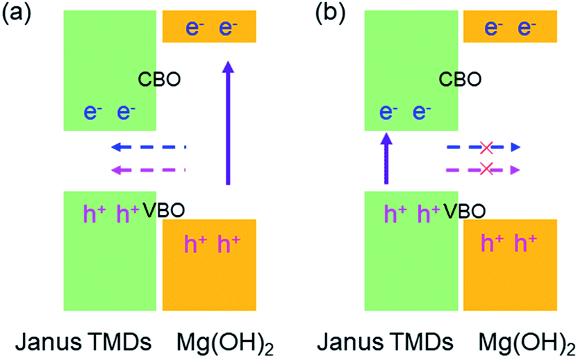 | ||
| Fig. 5 The band alignment schematic for the migration of free electrons and holes at the interface of the XSSe/Mg(OH)2 vdW heterostructure. | ||
Fig. 6(a) and (c) demonstrate the charge density difference between the interface of the XSSe and Mg(OH)2 layers, which shows that the MoSSe (or WSSe) layer acts as an electron-donor, while Mg(OH)2 layer receives the electrons. Furthermore, the Bader-charge analysis method87 was employed to quantitatively calculate the electron transfer, and the Mg(OH)2 layer obtained 0.003 (or 0.0042) |e| from the MoSSe (or WSSe) layer in their heterostructure. Such small electron transfers also explain the weak vdW forces between the interface of the XSSe/Mg(OH)2 vdW heterostructures. Besides, after the Janus TMDs contact with the Mg(OH)2 layer and reach an equilibrium, the potential differences between the interface of the heterostructure are addressed, as shown in Fig. 6(b) and (d). There is a potential drop between the interface calculated to be 11.59 and 11.44 eV for MoSSe/Mg(OH)2 and WSSe/Mg(OH)2 vdW heterostructures, respectively, which can also act as an effective driving force to promote the carrier in Fig. 5(a).
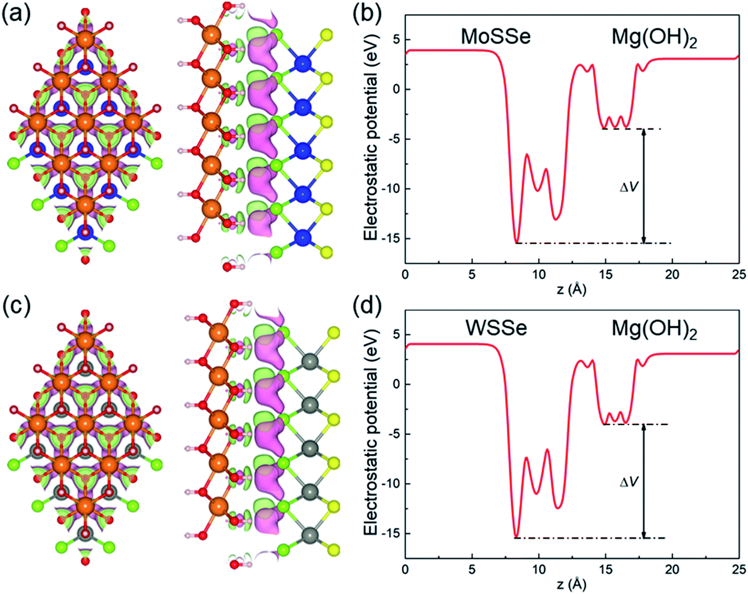 | ||
| Fig. 6 The isosurfaces of charge density difference of the (a) MoSSe/Mg(OH)2 and (c) WSSe/Mg(OH)2 vdW heterostructures, the obtaining and the losing of electrons are demonstrated by cyan and violet marks, respectively; the isosurface level of charge difference is set as 0.015 |e|; the calculated potential drop across interface of the (b) MoSSe/Mg(OH)2 and (d) WSSe/Mg(OH)2 vdW heterostructures. | ||
The light absorption capacity of the XSSe, Mg(OH)2 and the XSSe/Mg(OH)2 vdW heterostructure were investigated, as shown in Fig. 7. It is obvious that near the wavelength range of visible light (about 380–700 nm) the MoSSe, WSSe and XSSe/Mg(OH)2 vdW heterostructures exhibited an excellent optical absorption spectrum. In detail, the MoSSe/Mg(OH)2 and WSSe/Mg(OH)2 vdW heterostructures possessed pronounced absorption peaks of 5.496 × 105 cm−1 and 4.295 × 105 cm−1 at 352 nm and 367 nm, respectively. The XSSe/Mg(OH)2 vdW heterostructures displayed the ability to absorb sunlight absorption over a wide range in the visible and NIR regions, which considerably overlap the wavelength range of the solar spectrum. Besides, high absorption peaks appeared in the visible region approximately at the wavelengths of 562 and 495 nm for the MoSSe/Mg(OH)2 and WSSe/Mg(OH)2 vdW heterostructures by 1.432 × 105 cm−1 and 1.656 × 105 cm−1, respectively, which were higher than those of other TMD-based heterostructures, such as WS2/BSe (14.09 × 104 cm−1),88 g-GaN/BSe (1.470 × 105 cm−1)89 and g-GaN/BlueP (0.48 × 105 cm−1).45 The novel optical absorption characteristic of the XSSe/Mg(OH)2 vdW heterostructures also revealed their potential uses as optoelectronic devices.
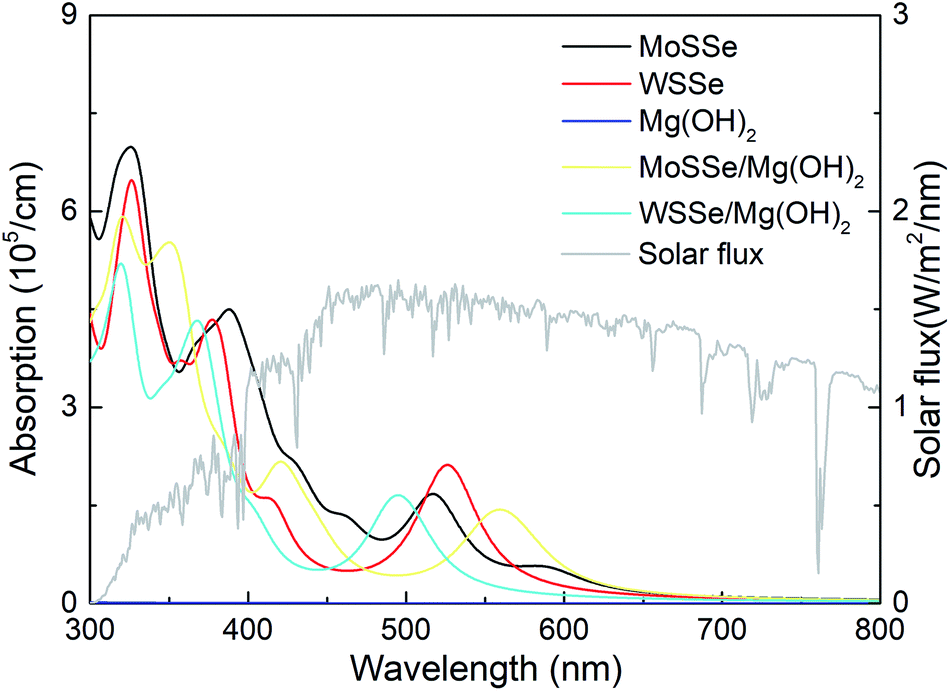 | ||
| Fig. 7 The optical absorption spectrum of the monolayered XSSe, Mg(OH)2 and XSSe/Mg(OH)2 vdW heterostructures calculated by the HSE06 functional. | ||
4. Conclusions
DFT calculations were explored systematically to study 2D heterostructures based on Janus TMDs and Mg(OH)2. The heterostructures of MoSSe/Mg(OH)2 and WSSe/Mg(OH)2 were formed by vdW forces with thermal and dynamic stability. Importantly, both XSSe/Mg(OH)2 vdW heterostructures possessed a semiconductor performance with direct bandgap values of 1.996 and 2.233 eV, respectively. The band alignment of the XSSe/Mg(OH)2 vdW heterostructure showed a type-I band structure for both heterostructures, which indicates that they are desirable candidates for light-emitting devices. Besides, the charge density difference analysis demonstrated that the MoSSe and WSSe layers donated 0.003 and 0.0042 |e| to the Mg(OH)2 layer in their heterostructures, respectively. Furthermore, both heterostructure had fantastic visible light absorptivity. The work provides a theoretical guidance to design new heterostructures based on Janus TMD materials for future nano-devices.Conflicts of interest
There are no conflicts to declare.Acknowledgements
This work was supported by the project of the Development and application of key equipment for intelligent spraying technology of automobile parts (00520088), the Development and application of complete set of intelligent testing equipment for automobile lamp (00520188) and the Open Fund Project of Maanshan Engineering Technology Research Center of Advanced Design for Automotive Stamping Dies (QMSG202105).References
- A. K. Geim and K. S. Novoselov, The rise of graphene, Nat. Mater., 2007, 6, 183–191 CrossRef CAS PubMed.
- M. D. Stoller, S. Park, Y. Zhu, J. An and R. S. Ruoff, Graphene-based ultracapacitors, Nano Lett., 2008, 8, 3498–3502 CrossRef CAS PubMed.
- J. Zhou, J. Lin, X. Huang, Y. Zhou, Y. Chen, J. Xia, H. Wang, Y. Xie, H. Yu, J. Lei, D. Wu, F. Liu, Q. Fu, Q. Zeng, C. H. Hsu, C. Yang, L. Lu, T. Yu, Z. Shen, H. Lin, B. I. Yakobson, Q. Liu, K. Suenaga, G. Liu and Z. Liu, A library of atomically thin metal chalcogenides, Nature, 2018, 556, 355–359 CrossRef CAS PubMed.
- H. Zhang, M. Chhowalla and Z. Liu, 2D nanomaterials: graphene and transition metal dichalcogenides, Chem. Soc. Rev., 2018, 47, 3015–3017 RSC.
- S. Zhou, Y. Guo and J. Zhao, Enhanced thermoelectric properties of graphene oxide patterned by nanoroads, Phys. Chem. Chem. Phys., 2016, 18, 10607–10615 RSC.
- L. Liu, X. Li, Z. Liu, S. Dai, X. Huang and J. Zhao, Tunable bending modulus and bending limit of oxidized graphene, Nanoscale, 2020, 12, 1623–1628 RSC.
- M. Sun, Q. Ren, Y. Zhao, J.-P. Chou, J. Yu and W. Tang, Electronic and magnetic properties of 4d series transition metal substituted graphene: A first-principles study, Carbon, 2017, 120, 265–273 CrossRef CAS.
- M. Sun, J. P. Chou, J. Yu and W. Tang, Electronic properties of blue phosphorene/graphene and blue phosphorene/graphene-like gallium nitride heterostructures, Phys. Chem. Chem. Phys., 2017, 19, 17324–17330 RSC.
- M. Sun, J. P. Chou, Y. Zhao, J. Yu and W. Tang, Weak C-HF-C hydrogen bonds make a big difference in graphane/fluorographane and fluorographene/fluorographane bilayers, Phys. Chem. Chem. Phys., 2017, 19, 28127–28132 RSC.
- R. Li, Y. Cheng and W. Huang, Recent Progress of Janus 2D Transition Metal Chalcogenides: From Theory to Experiments, Small, 2018, 14, e1802091 CrossRef PubMed.
- S. Z. Butler, S. M. Hollen, L. Cao, Y. Cui, J. A. Gupta, H. R. Gutiérrez, T. F. Heinz, S. S. Hong, J. Huang and A. F. Ismach, Progress, challenges, and opportunities in two-dimensional materials beyond graphene, ACS Nano, 2013, 7, 2898–2926 CrossRef CAS PubMed.
- Q. Liu, J. Xing, Z. Jiang, X. Jiang, Y. Wang and J. Zhao, 2D tetragonal transition-metal phosphides: an ideal platform to screen metal shrouded crystals for multifunctional applications, Nanoscale, 2020, 12, 6776–6784 RSC.
- J. Jiang, F. Sun, S. Zhou, W. Hu, H. Zhang, J. Dong, Z. Jiang, J. Zhao, J. Li and W. Yan, Atomic-level insight into super-efficient electrocatalytic oxygen evolution on iron and vanadium co-doped nickel (oxy) hydroxide, Nat. Commun., 2018, 9, 1–12 CrossRef PubMed.
- Y. Guo, L. Ma, K. Mao, M. Ju, Y. Bai, J. Zhao and X. C. Zeng, Eighteen functional monolayer metal oxides: wide bandgap semiconductors with superior oxidation resistance and ultrahigh carrier mobility, Nanoscale Horiz., 2019, 4, 592–600 RSC.
- S. Zhou, N. Liu and J. Zhao, Phosphorus quantum dots as visible-light photocatalyst for water splitting, Comput. Mater. Sci., 2017, 130, 56–63 CrossRef CAS.
- Y. Gao, D. Sun, X. Jiang and J. Zhao, Point defects in group III nitrides: A comparative first-principles study, J. Appl. Phys., 2019, 125, 215705 CrossRef.
- S. Zhou and J. Zhao, Two-dimensional B–C–O alloys: a promising class of 2D materials for electronic devices, Nanoscale, 2016, 8, 8910–8918 RSC.
- Y. Li, Q. Cui, F. Ceballos, S. D. Lane, Z. Qi and H. Zhao, Ultrafast Interlayer Electron Transfer in Incommensurate Transition Metal Dichalcogenide Homobilayers, Nano Lett., 2017, 17, 6661–6666 CrossRef CAS PubMed.
- Y. Cai, J. Lan, G. Zhang and Y.-W. Zhang, Lattice vibrational modes and phonon thermal conductivity of monolayer MoS2, Phys. Rev. B, 2014, 89, 035438 CrossRef.
- K. Ren, M. Sun, Y. Luo, S. Wang, J. Yu and W. Tang, First-principle study of electronic and optical properties of two-dimensional materials-based heterostructures based on transition metal dichalcogenides and boron phosphide, Appl. Surf. Sci., 2019, 476, 70–75 CrossRef CAS.
- D. Y. Qiu, H. Felipe and S. G. Louie, Optical spectrum of MoS2: many-body effects and diversity of exciton states, Phys. Rev. Lett., 2013, 111, 216805 CrossRef PubMed.
- K. Chen, D. Kiriya, M. Hettick, M. Tosun, T.-J. Ha, S. R. Madhvapathy, S. Desai, A. Sachid and A. Javey, Air stable n-doping of WSe2 by silicon nitride thin films with tunable fixed charge density, APL Mater., 2014, 2, 092504 CrossRef.
- D. Wickramaratne, F. Zahid and R. K. Lake, Electronic and thermoelectric properties of few-layer transition metal dichalcogenides, J. Chem. Phys., 2014, 140, 124710 CrossRef PubMed.
- B. Radisavljevic, A. Radenovic, J. Brivio, V. Giacometti and A. Kis, Single-layer MoS2 transistors, Nat. Nanotechnol., 2011, 6, 147–150 CrossRef CAS PubMed.
- S. Zhou and J. Zhao, Electronic structures of germanene on MoS2: effect of substrate and molecular adsorption, J. Phys. Chem. C, 2016, 120, 21691–21698 CrossRef CAS.
- S. Zhou, N. Liu, Z. Wang and J. Zhao, Nitrogen-doped graphene on transition metal substrates as efficient bifunctional catalysts for oxygen reduction and oxygen evolution reactions, ACS Appl. Mater. Interfaces, 2017, 9, 22578–22587 CrossRef CAS PubMed.
- Y. Luo, S. Wang, H. Shu, J.-P. Chou, K. Ren, J. Yu and M. Sun, A MoSSe/blue phosphorene vdw heterostructure with energy conversion efficiency of 19.9% for photocatalytic water splitting, Semicond. Sci. Technol., 2020, 35, 125008 CrossRef CAS.
- M. Sun, J.-P. Chou, A. Hu and U. Schwingenschlögl, Point Defects in Blue Phosphorene, Chem. Mater., 2019, 31, 8129–8135 CrossRef CAS.
- J. Li, Z. Huang, W. Ke, J. Yu, K. Ren and Z. Dong, High solar-to-hydrogen efficiency in Arsenene/GaX (X = S, Se) van der Waals heterostructure for photocatalytic water splitting, J. Alloys Compd., 2021, 866 Search PubMed.
- M. Sun, J.-P. Chou, J. Yu and W. Tang, Effects of structural imperfection on the electronic properties of graphene/WSe2 heterostructures, J. Mater. Chem. C, 2017, 5, 10383–10390 RSC.
- S. Wang, C. Ren, H. Tian, J. Yu and M. Sun, MoS2/ZnO van der Waals heterostructure as a high-efficiency water splitting photocatalyst: a first-principles study, Phys. Chem. Chem. Phys., 2018, 20, 13394–13399 RSC.
- M. Sun and U. Schwingenschlögl, B2P6: A Two-Dimensional Anisotropic Janus Material with Potential in Photocatalytic Water Splitting and Metal-Ion Batteries, Chem. Mater., 2020, 32, 4795–4800 CrossRef CAS.
- M. Sun, Y. Yan and U. Schwingenschlögl, Beryllene: A Promising Anode Material for Na-and K-Ion Batteries with Ultrafast Charge/Discharge and High Specific Capacity, J. Phys. Chem. Lett., 2020, 11, 9051–9056 CrossRef CAS PubMed.
- M. Sun and U. Schwingenschlögl, Structure Prototype Outperforming MXenes in Stability and Performance in Metal-Ion Batteries: A High Throughput Study, Advanced Energy Materials, 2021 Search PubMed.
- M. Sun and U. Schwingenschlögl, Unique Omnidirectional Negative Poisson's Ratio in δ-Phase Carbon Monochalcogenides, J. Phys. Chem. C, 2021, 125, 4133–4138 CrossRef CAS.
- M. Sun and U. Schwingenschlögl, δ-CS: A Direct-Band-Gap Semiconductor Combining Auxeticity, Ferroelasticity, and Potential for High-Efficiency Solar Cells, Phys. Rev. Appl., 2020, 14, 044015 CrossRef CAS.
- H. Wang, X. Li, P. Li and J. Yang, δ-Phosphorene: a two dimensional material with a highly negative Poisson's ratio, Nanoscale, 2017, 9, 850–855 RSC.
- H. Zhang, Y. Li, J. Hou, A. Du and Z. Chen, Dirac State in the FeB2 Monolayer with Graphene-Like Boron Sheet, Nano Lett., 2016, 16, 6124–6129 CrossRef CAS PubMed.
- T. Yu, Z. Zhao, L. Liu, S. Zhang, H. Xu and G. Yang, TiC3 Monolayer with High Specific Capacity for Sodium-Ion Batteries, J. Am. Chem. Soc., 2018, 140, 5962–5968 CrossRef CAS PubMed.
- B. Wang, Q. Wu, Y. Zhang, Y. Guo, X. Zhang, Q. Zhou, S. Dong and J. Wang, High Curie-temperature intrinsic ferromagnetism and hole doping-induced half-metallicity in two-dimensional scandium chlorine monolayers, Nanoscale Horiz., 2018, 3, 551–555 RSC.
- K. S. Novoselov, A. Mishchenko, A. Carvalho and A. H. Castro Neto, 2D materials and van der Waals heterostructures, Science, 2016, 353, aac9439 CrossRef CAS PubMed.
- D. L. Duong, S. J. Yun and Y. H. Lee, van der Waals Layered Materials: Opportunities and Challenges, ACS Nano, 2017, 11, 11803–11830 CrossRef CAS PubMed.
- K. Ren, R. Zheng, P. Xu, D. Cheng, W. Huo, J. Yu, Z. Zhang and Q. Sun, Electronic and Optical Properties of Atomic-Scale Heterostructure Based on MXene and MN (M = Al, Ga): A DFT Investigation, Nanomaterials, 2021, 11(9), 2236 CrossRef.
- K. Ren, K. Wang, Y. Cheng, W. Tang and G. Zhang, Two-dimensional heterostructures for photocatalytic water splitting: a review of recent progress, Nano Futures, 2020, 4, 032006 CrossRef CAS.
- K. Ren, S. Wang, Y. Luo, Y. Xu, M. Sun, J. Yu and W. Tang, Strain-enhanced properties of van der Waals heterostructure based on blue phosphorus and g-GaN as a visible-light-driven photocatalyst for water splitting, RSC Adv., 2019, 9, 4816–4823 RSC.
- Y. Yan, Z. Zeng, M. Huang and P. Chen, Van der waals heterojunctions for catalysis, Mater. Today Adv., 2020, 6, 100059 CrossRef.
- K. Ren, W. Tang, M. Sun, Y. Cai, Y. Cheng and G. Zhang, A direct Z-scheme PtS2/arsenene van der Waals heterostructure with high photocatalytic water splitting efficiency, Nanoscale, 2020, 12, 17281–17289 RSC.
- Y. Liu, N. O. Weiss, X. Duan, H.-C. Cheng, Y. Huang and X. Duan, Van der Waals heterostructures and devices, Nat. Rev. Mater., 2016, 1, 16042 CrossRef CAS.
- R. Kumar, D. Das and A. K. Singh, C2N/WS2 van der Waals type-II heterostructure as a promising water splitting photocatalyst, J. Catal., 2018, 359, 143–150 CrossRef CAS.
- R. Zhang, L. Zhang, Q. Zheng, P. Gao, J. Zhao and J. Yang, Direct Z-scheme water splitting photocatalyst based on two-dimensional Van Der Waals heterostructures, J. Phys. Chem. Lett., 2018, 9, 5419–5424 CrossRef CAS PubMed.
- R. Shi, F. Liu, Z. Wang, Y. Weng and Y. Chen, Black/red phosphorus quantum dots for photocatalytic water splitting: from a type I heterostructure to a Z-scheme system, Chem. Commun., 2019, 55, 12531–12534 RSC.
- T. Yamaoka, H. E. Lim, S. Koirala, X. Wang, K. Shinokita, M. Maruyama, S. Okada, Y. Miyauchi and K. Matsuda, Efficient Photocarrier Transfer and Effective Photoluminescence Enhancement in Type I Monolayer MoTe2/WSe2 Heterostructure, Adv. Funct. Mater., 2018, 28, 1801021 CrossRef.
- W. Zheng, B. Zheng, Y. Jiang, C. Yan, S. Chen, Y. Liu, X. Sun, C. Zhu, Z. Qi, T. Yang, W. Huang, P. Fan, F. Jiang, X. Wang, X. Zhuang, D. Li, Z. Li, W. Xie, W. Ji, X. Wang and A. Pan, Probing and Manipulating Carrier Interlayer Diffusion in van der Waals Multilayer by Constructing Type-I Heterostructure, Nano Lett., 2019, 19, 7217–7225 CrossRef CAS PubMed.
- M. Z. Bellus, M. Li, S. D. Lane, F. Ceballos, Q. Cui, X. C. Zeng and H. Zhao, Type-I van der Waals heterostructure formed by MoS2 and ReS2 monolayers, Nanoscale Horiz., 2017, 2, 31–36 RSC.
- M. Virgilio and G. Grosso, Type-I alignment and direct fundamental gap in SiGe based heterostructures, J. Phys.: Condens. Matter, 2006, 18, 1021–1031 CrossRef CAS.
- D. Dorfs, T. Franzl, R. Osovsky, M. Brumer, E. Lifshitz, T. A. Klar and A. Eychmuller, Type-I and type-II nanoscale heterostructures based on CdTe nanocrystals: a comparative study, Small, 2008, 4, 1148–1152 CrossRef CAS PubMed.
- T.-N. Do, M. Idrees, N. T. T. Binh, H. V. Phuc, N. N. Hieu, L. T. Hoa, B. Amin and H. Van, Type-I band alignment of BX–ZnO (X = As, P) van der Waals heterostructures as high-efficiency water splitting photocatalysts: a first-principles study, RSC Adv., 2020, 10, 44545–44550 RSC.
- L. Ju, M. Bie, X. Zhang, X. Chen and L. Kou, Two-dimensional Janus van der Waals heterojunctions: A review of recent research progresses, Front. Phys., 2021, 16, 1–16 CrossRef.
- J. Zhang, S. Jia, I. Kholmanov, L. Dong, D. Er, W. Chen, H. Guo, Z. Jin, V. B. Shenoy, L. Shi and J. Lou, Janus Monolayer Transition-Metal Dichalcogenides, ACS Nano, 2017, 11, 8192–8198 CrossRef CAS PubMed.
- A. Y. Lu, H. Zhu, J. Xiao, C. P. Chuu, Y. Han, M. H. Chiu, C. C. Cheng, C. W. Yang, K. H. Wei, Y. Yang, Y. Wang, D. Sokaras, D. Nordlund, P. Yang, D. A. Muller, M. Y. Chou, X. Zhang and L. J. Li, Janus monolayers of transition metal dichalcogenides, Nat. Nanotechnol., 2017, 12, 744–749 CrossRef CAS PubMed.
- J. Wang, H. Shu, T. Zhao, P. Liang, N. Wang, D. Cao and X. Chen, Intriguing electronic and optical properties of two-dimensional Janus transition metal dichalcogenides, Phys. Chem. Chem. Phys., 2018, 20, 18571–18578 RSC.
- W.-J. Yin, X.-L. Zeng, B. Wen, Q.-X. Ge, Y. Xu, G. Teobaldi and L.-M. Liu, The unique carrier mobility of Janus MoSSe/GaN heterostructures, Front. Phys., 2021, 16, 1–9 Search PubMed.
- P. Zhao, Y. Liang, Y. Ma, B. Huang and Y. Dai, Janus Chromium Dichalcogenide Monolayers with Low Carrier Recombination for Photocatalytic Overall Water-Splitting under Infrared Light, J. Phys. Chem. C, 2019, 123, 4186–4192 CrossRef CAS.
- X. Ma, X. Wu, H. Wang and Y. Wang, A Janus MoSSe monolayer: a potential wide solar-spectrum water-splitting photocatalyst with a low carrier recombination rate, J. Mater. Chem. A, 2018, 6, 2295–2301 RSC.
- D. Er, H. Ye, N. C. Frey, H. Kumar, J. Lou and V. B. Shenoy, Prediction of Enhanced Catalytic Activity for Hydrogen Evolution Reaction in Janus Transition Metal Dichalcogenides, Nano Lett., 2018, 18, 3943–3949 CrossRef CAS PubMed.
- C. Xia, W. Xiong, J. Du, T. Wang, Y. Peng and J. Li, Universality of electronic characteristics and photocatalyst applications in the two-dimensional Janus transition metal dichalcogenides, Phys. Rev. B, 2018, 98, 165424 CrossRef CAS.
- A. Suslu, K. Wu, H. Sahin, B. Chen, S. Yang, H. Cai, T. Aoki, S. Horzum, J. Kang, F. M. Peeters and S. Tongay, Unusual dimensionality effects and surface charge density in 2D Mg(OH)2, Sci. Rep., 2016, 6, 20525 CrossRef CAS PubMed.
- K. Ren, J. Yu and W. Tang, First-principles study of two-dimensional van der Waals heterostructure based on ZnO and Mg(OH)2: A potential photocatalyst for water splitting, Phys. A, 2019, 125916 CAS.
- K. Ren, J. Yu and W. Tang, A two-dimensional vertical van der Waals heterostructure based on g-GaN and Mg(OH)2 used as a promising photocatalyst for water splitting: A first-principles calculation, J. Appl. Phys., 2019, 126, 065701 CrossRef.
- F. Li, W. Wei, P. Zhao, B. Huang and Y. Dai, Electronic and Optical Properties of Pristine and Vertical and Lateral Heterostructures of Janus MoSSe and WSSe, J. Phys. Chem. Lett., 2017, 8, 5959–5965 CrossRef CAS PubMed.
- T. Jing, D. Liang, J. Hao, M. Deng and S. Cai, Interface Schottky barrier in Hf2NT2/MSSe (T = F, O, OH; M = Mo, W) heterostructures, Phys. Chem. Chem. Phys., 2019, 5394–5401 RSC.
- Y. Liang, J. Li, H. Jin, B. Huang and Y. Dai, Photoexcitation Dynamics in Janus-MoSSe/WSe2 Heterobilayers: Ab Initio Time-Domain Study, J. Phys. Chem. Lett., 2018, 9, 2797–2802 CrossRef CAS PubMed.
- Y. Li, J. Wang, B. Zhou, F. Wang, Y. Miao, J. Wei, B. Zhang and K. Zhang, Tunable interlayer coupling and Schottky barrier in graphene and Janus MoSSe heterostructures by applying an external field, Phys. Chem. Chem. Phys., 2018, 20, 24109–24116 RSC.
- S. Grimme, J. Antony, S. Ehrlich and H. Krieg, A consistent and accurate ab initio parametrization of density functional dispersion correction (DFT-D) for the 94 elements H-Pu, J. Chem. Phys., 2010, 132, 154104 CrossRef PubMed.
- G. Kresse and J. Furthmüller, Efficiency of ab-initio total energy calculations for metals and semiconductors using a plane-wave basis set, Comput. Mater. Sci., 1996, 6, 15–50 CrossRef CAS.
- G. Kresse and J. Furthmüller, Efficient iterative schemes for ab initio total-energy calculations using a plane-wave basis set, Phys. Rev. B, 1996, 54, 11169 CrossRef CAS PubMed.
- G. Kresse and D. Joubert, From ultrasoft pseudopotentials to the projector augmented-wave method, Phys. Rev. B, 1999, 59, 1758 CrossRef CAS.
- J. Heyd, G. E. Scuseria and M. Ernzerhof, Hybrid functionals based on a screened Coulomb potential, J. Chem. Phys., 2003, 118, 8207–8215 CrossRef CAS.
- S. Grimme, Semiempirical GGA-type density functional constructed with a long-range dispersion correction, J. Comput. Chem., 2006, 27, 1787–1799 CrossRef CAS PubMed.
- A. Togo and I. J. S. M. Tanaka, First principles phonon calculations in materials science, Scr. Mater., 2015, 108, 1–5 CrossRef CAS.
- A. Togo, F. Oba and I. J. P. R. B. Tanaka, First-principles calculations of the ferroelastic transition between rutile-type and CaCl2-type SiO2 at high pressures, Phys. Rev. B, 2008, 78, 134106 CrossRef.
- K. Ren, S. Wang, Y. Luo, J.-P. Chou, J. Yu, W. Tang and M. Sun, High-efficiency photocatalyst for water splitting: a Janus MoSSe/XN (X = Ga, Al) van der Waals heterostructure, J. Phys. D: Appl. Phys., 2020, 53, 185504 CrossRef CAS.
- X. Chen, F. Tian, C. Persson, W. Duan and N. X. Chen, Interlayer interactions in graphites, Sci. Rep., 2013, 3, 3046 CrossRef PubMed.
- T. Bjorkman, A. Gulans, A. V. Krasheninnikov and R. M. Nieminen, van der Waals bonding in layered compounds from advanced density-functional first-principles calculations, Phys. Rev. Lett., 2012, 108, 235502 CrossRef CAS PubMed.
- S. Nosé, A unified formulation of the constant temperature molecular dynamics methods, J. Chem. Phys., 1984, 81, 511–519 CrossRef.
- Z. Lu, D. Lockwood and J.-M. Baribeau, Quantum confinement and light emission in SiO2/Si superlattices, Nature, 1995, 378, 258–260 CrossRef CAS.
- W. Tang, E. Sanville and G. Henkelman, A grid-based Bader analysis algorithm without lattice bias, J. Phys.: Condens. Matter, 2009, 21, 084204 CrossRef CAS PubMed.
- Y. Luo, K. Ren, S. Wang, J.-P. Chou, J. Yu, Z. Sun and M. Sun, First-Principles Study on Transition-Metal Dichalcogenide/BSe van der Waals Heterostructures: A Promising Water-Splitting Photocatalyst, J. Phys. Chem. C, 2019, 123, 22742–22751 CrossRef CAS.
- K. Ren, Y. Luo, S. Wang, J.-P. Chou, J. Yu, W. Tang and M. Sun, A van der Waals Heterostructure Based on Graphene-like Gallium Nitride and Boron Selenide: A High-Efficiency Photocatalyst for Water Splitting, ACS Omega, 2019, 4, 21689–21697 CrossRef CAS PubMed.
| This journal is © The Royal Society of Chemistry 2021 |