
 Open Access Article
 This Open Access Article is licensed under a Creative Commons Attribution-Non Commercial 3.0 Unported Licence
Optimum fabrication parameters for preparing high performance SERS substrates based on Si pyramid structure and silver nanoparticles
Nguyen Thuy Ngoc Thuya,
Huynh Nguyen Thanh Luanbc,
Van Vo Kim Hieubd,
Mai Thi Thanh Ngan a,
Nguyen Tri Trunga,
Le Vu Tuan Hungbe and
Tran T. T. Van*bc
a,
Nguyen Tri Trunga,
Le Vu Tuan Hungbe and
Tran T. T. Van*bc
aFaculty of Applied Sciences, HCMC University of Technology and Education, Vietnam
bFaculty of Materials Science and Technology, University of Science, VNU-HCM, Vietnam. E-mail: tttvan@hcmus.edu.vn
cVietnam National University, Ho Chi Minh City, Vietnam
dTribology Lab, Department of Mechanical Engineering, University of Ulsan, 93 Daehak-ro, Nam-gu, Ulsan 44610, South Korea
eFaculty of Physics and Engineering Physics, University of Science, VNU-HVM, Vietnam
First published on 22nd September 2021
Abstract
In this work, we propose simple and inexpensive methods to prepare micro/nano hierarchical Surface-Enhanced Raman Scattering (SERS) substrates, in which pyramid structure is created by using anisotropic wet etching of a silicon wafer and a silver thin film is deposited on these pyramid arrays by thermal evaporation. The ensemble is then annealed at 450 °C for 2 hours to form silver nanoparticles (AgNPs). The sizes and density of the pyramids and AgNPs are optimized mainly by changing the etching temperature (60–80 °C), the thickness of the Ag-film (15–45 nm) and etching time (3–10 min). The ultraviolet visible (UV-Vis) absorbance spectra show that the AgNPs formed with the 30 nm-thick film exhibit the strongest plasmonic effect. Under these conditions, the spherical AgNPs with sizes of 42–48 nm are densely distributed on the silicon micro-pyramid array. The obtained SERS signal is the strongest at the pyramid base-edge size of 7–10 μm. The enhancement factor obtained from the abamectin probe molecules is as high as 1 × 10⁶ and the SERS substrates enable the detection of abamectin concentrations as low as 5.7 × 10⁻⁹ M. Therefore, this work provides a novel SERS substrate structure that has a high potential for use in medicine and biotechnology or as a food security sensor.
Introduction
Abamectin (avermectin B1) was first introduced in 1985 as a crop insecticide against mites and some insect species. According to the criteria for the EU classification of dangerous substances (EC 2001), abamectin should be classified as very toxic to aquatic organisms. Although low concentrations of abamectin are expected in water bodies, very low concentrations of abamectin could also cause toxic effects on some sensitive aquatic organisms.1–3 The detection of trace quantities of abamectin usually employs expensive equipment such as liquid chromatography mass spectrometry (LC-MS), high-performance liquid chromatography (HPLC), etc. It is necessary to develop high throughput and cost-effective methods for screening these residues. The Surface-Enhanced Raman Spectroscopy (SERS) technique meets these requirements because it is a very fast and sensitive method of detecting chemicals and biomolecules.Some authors have shown that strong localized surface plasmon resonance (LSPR) occurs at the nanoscale of noble metals, which can greatly improve the SERS signal (SERS hot spots).4–17 There are two mechanisms for increasing SERS signal widely accepted. Those are electromagnetic (EM) enhancement and chemical enhancement. The EM enhancement is related to the excitation of LSPR of the metal nanostructures. At this time, the magnitude of the EM field at proximity places around the metal nanostructure increase significantly. Meanwhile, the chemical enhancement associated with the charge transfer mechanism between the target molecule and SERS substrates due to the chemisorption of target molecules on the metal nanostructures. However, the chemical enhancement mechanism is molecule specific and typically gives a much lower enhancement factor compared to the EM enhancement. Moreover, studies have shown that the SERS signal can be improved in 3D microstructure substrates, for example, ZnO nanoflower,18 nanowires, nanorod,19 TiO2 nanowires,20 flower-like alumina,21 silicon nanowire and pyramid structures,5,8,9 due to their large surface areas for more metal particles loading and light-trapping effects. To generate very strong SERS signals, the combination of the 3D microstructure substrates and the strong local plasmons resonance of nanoparticles emerges as a novel solution. Such micro/nano hierarchical structures have been reported by other authors.5,8,9,22 Among them, 3D SERS substrates based on silicon pyramid loading silver nanoparticles (AgNPs@PSi) reveal high enhancement factor, reliability and repeatability compared with other dimensional substrates. Many researches on AgNPs@PSi have been recently reported.8,23,24 Most of them focus on the mechanism of SERS effect and the control of AgNPs size. However, there are still several points remained to be solved: (1) the spatial gap between AgNPs is not small enough to active as “hot spots”, (2) how to control the growth of AgNPs without agglomeration. Interestingly, these points are directly related to the pyramids size. In this work, the mechanism for improving SERS signals related to the size of pyramids, the size of AgNPs, and the gap among AgNPs have been discussed also in detail.
In the present work, we provide simple method to prepare silver nanoparticles (AgNPs) on silicon pyramid substrates for the enhancement of SERS signals. We use silicon anisotropic wet-etching in solution containing KOH (potassium hydroxide) and IPA (isopropyl alcohol) to produce a random pyramid structure on a silicon wafer and then use the thermal evaporation deposition to create a silver film on the pyramid substrates, then a heat treatment to form AgNPs. In fact, there are so many methods to fabricate AgNPs reported for years.14,25–27 Each method has own advantages or disadvantages. The thermal evaporation method to create AgNPs from initial Ag film is simple and has no impurities affect. In our work, the pyramid and AgNPs sizes were controlled by changing experimental parameters such as the etching temperatures, etching time and thickness of Ag film, respectively. Finally, we applied the prepared SERS substrates to detect abamectin solutions. The results indicate that the optimum substrates have high sensitivity and can detect abamectin at concentrations as low as 5.7 × 10⁻⁹ M. In addition, the correlation between pyramid size and enhancement effect have been demonstrated.
Experimental and characterization
Materials
The planar Si wafers were purchased from MTI Corporation (USA). Methanol, isopropyl alcohol, hydrochloric acid 37%, hydrofluoric acid 43%, acetone and H2O2 were purchased from Merck (Germany). Potassium hydroxide was supplied by VWR Chemical (Belgium). Abamectin for Raman measurements was purchased from Sigma Aldrich (USA). The deionized (DI) water used in experimental process was obtained from a Millipore Purification System with a resistivity of 18.2 MΩ cm−1.Sample preparation
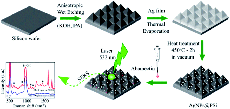
The preparation process of AgNPs on Si pyramid (AgNPs@PSi) substrate is presented in Fig. 1. The substrates were fabricated by using chemical wet-etching of (100) silicon wafers in KOH and IPA solutions. Firstly, the Si wafers were cleaned in an ultrasonic bath using acetone, alcohol and deionized water for 5 min, each. Subsequently, the samples were immersed in a (HCl![[thin space (1/6-em)]](https://www.rsc.org/images/entities/char_2009.gif) :H2O2) solution for 10 s to remove organic residues and metal ion impurities. For the next step, the samples were dipped in a dilute 10% HF solution for removal of the thin silicon oxide layer on the surface of the Si wafers.
:H2O2) solution for 10 s to remove organic residues and metal ion impurities. For the next step, the samples were dipped in a dilute 10% HF solution for removal of the thin silicon oxide layer on the surface of the Si wafers.
 | ||
| Fig. 1 The preparation process of AgNPs on Si pyramid, denoted as (AgNPs@PSi) substrates. | ||
After this cleaning process, the samples were anisotropically etched in a solution containing KOH and IPA. As a result of the etching process, pyramids were formed on the surface of the Si substrates. The number and size of the pyramids on the Si surface can be controlled by the etching conditions such as etching time, etching temperature, and KOH/IPA concentrations. In the present work, the etching temperatures were 60 °C, 70 °C, and 80 °C; the etching time varied from 3 to 10 min; the composition of the solution was KOH (4 M) and IPA (0.65 M).
AgNPs were fabricated thermally on Si pyramid substrates for the detection of abamectin and on quartz substrates for UV-visible measurements to investigate the plasmonic effect of these AgNPs. Firstly, a thin film of silver was deposited on the Si/quartz substrate by thermal evaporation (GSL-1700X-SPC-2 from MTI). Then the samples were annealed in vacuum (10 mTorr) at a temperature in the range of 400500 °C for AgNPs formation. The annealing time varied from one hour to three hours. By controlling the experimental parameters of silver thin film thickness, annealing time and annealing temperature, the nearly spherical shape AgNPs can be fabricated at the optimal experimental conditions. These spherical AgNPs give a highly efficient plasmonic effect, as shown clearly in the UV-visible measurements.
In this work, the insecticide abamectin was used as a target molecule. A range of concentrations from 5.7 × 10⁻⁹ M to 1.14 × 10⁻⁵ M of aqueous solutions of abamectin, was prepared for SERS testing on AgNPs@PSi substrates. A 30 μl drop of abamectin was deposited and spread out on each SERS substrate. After they were completely dried, Raman spectra were measured.
Characterization
Field-emission-scanning electron microscopy (FESEM, Hitachi S4800) and optical microscopy (OM, Olympus MX51) were chosen to characterize the surface morphology of the PSi/AgNPs@PSi substrates. The crystalline quality and the single-crystalline structure of AgNPs@PSi and PSi were characterized using a Bruker D8 Advance diffractometer. For this work, a copper sealed-tube X-ray source produced Cu Kα radiation at a wavelength of 1.5406 Å. The generator operated at 40 kV and 40 mA.The plasmonic effect of AgNPs was investigated using UV-Visible measurements (Jasco V-730). Raman spectra were recorded using a Raman microscope system (XploRA plus, Horiba) with laser excitation at 532 nm.
The AgNPs diameter and the nearest-neighbor distance between AgNPs were calculated from FESEM images using ImageJ sofware. In this case, each silver particle was considered as a sphere and the diameter D of particle was obtained through its area A. To improve the precision, area A of separated grains with high contrast were selected. The diameter D was deduced from area A via  . To the nearest distance, the “ND plugin” was used to determine the spacing d between grain boundaries as
  , in which (x, y) is centroid coordinates of each AgNPs, r is the radius of AgNPs.28 The coordination number 5 is preferred in the present work.
Results and discussion
Pyramid formation on Si substrates
Several papers have reported on Si anisotropic etching using KOH solutions in presence of IPA.9,29,30 The etching rate on the crystal orientations (100), (110), and (111) is different due to the different number of back-bonds of Si atoms on the surface. Each Si atom on the surface of a Si (100) wafer has two back-bonds which connect to underlying silicon atoms and two dangling bonds; while that of Si (110) or Si (111) has three back-bonds and one dangling bond. Therefore, the removal of one Si atom from the (100) plane is easier compared to that from the (110) or (111) planes. As a result, the wet-etching processes take place much faster along the [100] directions compared to others. With different surface orientations of a Si wafer, wet-etching with a KOH solution will give different etched-Si surface morphologies. In the present work, the Si (100) orientation was used for anisotropic etching in order to obtain the formation of pyramids on the surface. As etching occurred mainly along the [100] direction and stopped at the (111) plane, the pyramids formed on the Si surface had (100) orientation as the base plane and (111) as the edge plane.The Si wafers are etched only by OH− radicals. The role of IPA is to reduce the etching rate, which yields anisotropic etching and leads to the easy and clear formation of pyramid shapes. In the etching process, there are hydrogen bubbles formed on the surface that can prevent the approach of OH− radicals to the surface. For this reason, the resulting pyramid shapes are not perfect. To minimize this effect, the Si wafers were shaken softly after being dipped into the etching solution, so as to remove hydrogen bubbles.
The etching conditions include etching temperature, etching time, and the concentrations of KOH and IPA. The purpose of the present work was to optimize these experimental conditions, so as to obtain good pyramid shapes, high density of pyramids on the surface and controlled pyramid size. The concentration of the KOH/IPA solution was kept at KOH (4 M) and IPA (0.65 M) which is commonly used for Si wet etching.29,30 For investigating the effect of the etching time on pyramid formation, the etching time was varied from 3 to 10 minutes (Fig. 2).
 | ||
| Fig. 2 OM images of PSi with various etching time and the etching temperature of 70 °C (a) 3 min, (b) 5 min, (c) 7 min, (d) 10 min. | ||
The results showed that the etching time has little effect on pyramid size, but that it plays an important role on the density of pyramids formed. For the present research, the optimized etching time for obtaining a very dense formation of pyramids was found to be 7 minutes. The etching rate depends strongly on temperature and the etching temperature mainly determines the size of pyramids. If the etching temperature is lower than 60 °C, the pyramid size is around 1 μm, which gives a very weak effect on SERS signal. On the other hand, if the etching temperature is higher than 80 °C, the IPA evaporates too quickly and the reaction rate is so fast that pyramids are no longer formed. Here, the etching temperatures of 60 °C, 70 °C, and 80 °C were chosen for detailed investigations.
According to the FESEM and OM images of Fig. 3, the length of the base-edge is around 1–3 μm, 3–7 μm and 7–10 μm at 60 °C, 70 °C, and 80 °C, respectively. This data indicates that the higher the etching temperature, the larger the pyramid. So the 3D pyramid-microstructure size can be controlled with the appropriate etching temperature. From these images, one can see that the Si pyramids are densely and randomly distributed on the wafer surface, thus exhibiting a perfect surface texture. Zhong et al. reported that such random-sized pyramid array can collect light over a wide wavelength range more efficiently than a planar structure or even a single-sized pyramid array.31
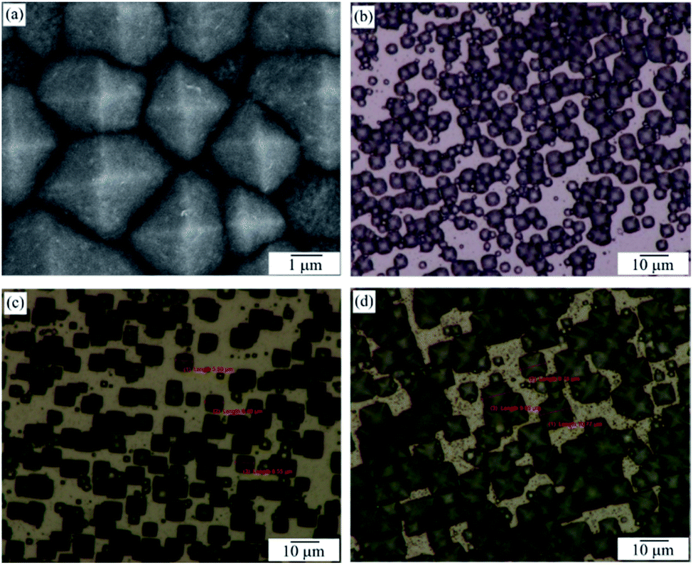 | ||
| Fig. 3 FESEM image of PSi with etching temperature of 60 °C (a); OM images of PSi with various etching temperatures (b) 60 °C, (c) 70 °C, (d) 80 °C. | ||
Reflectance spectra
To evaluate the optical performance of the substrates, the reflectance spectra of substrates with different pyramid sizes are compared in Fig. 4. | ||
| Fig. 4 Reflectance spectra of flat Si substrate and PSi substrates with various pyramid sizes. The inset image is AFM image in 3D of PSi substrate with pyramid size of 3–7 μm. | ||
The flat Si substrate has the highest reflectance of around 40% in the spectral range from 500 to 900 nm due to its much smoother surface. The formation of pyramids on substrates (as shown in the inset image of Fig. 4) leads to a significant reduction of surface reflectance. When the pyramid size is in range of 7–10 μm, the reflectance is only 6%. These results are in a good agreement with those reported by other authors.31,32 This result indicates that PSi substrates can trap the incident light effectively for scattering and absorbance. The larger the pyramid size, the greater the scattering effect. This observation is very useful for modelling an increase of the SERS signal.
UV-Vis spectroscopy
UV-Vis absorption spectroscopy was also utilized to investigate the plasmonic effects of AgNPs. Noble metal nanoparticles exhibit strongly localized surface plasmon resonance (LSPR), which is a collective oscillation of free electrons on the surface of metal nanoparticles during irradiation. Due to the external electric field of the incident light, the collective motion of free electrons results in a polarization which acts as a restoring force for oscillation. Resonance occurs when the frequency of the collective oscillation is equal to that of the incident light. With resonance, the incident light is strongly absorbed and scattered, which results in a corresponding peak in the UV-Vis spectrum. The intensity of the electromagnetic field may be significantly larger than that of the incident light.The resonance frequency depends strongly on nanoparticle size, shape and its environment. In fact, the resonance happens only if the noble metal nanoparticles are small enough comparable to wavelength of incident light and decay quickly with much increased particle size. For a deep investigation of AgNPs surface plasmons, the AgNPs were prepared on quartz substrates under various experimental conditions. Hence, variations were made of the silver thin-film thickness, corresponding to deposition time of 10, 20 and 30 s, annealing time of 1, 2 and 3 h and temperatures of 400, 450 and 500 °C.
Fig. 5 presents the UV-Vis spectra of the silver film with a deposition time of 20 s, before and after a heat treatment at 450 °C for 2 h. The FESEM images of silver film and of AgNPs formed after annealing are also inserted. The absorbance curve of a silver thin film without annealing is characteristic of a metallic mirror. The cross-section FE-SEM image of a silver thin film on a flat silicon substrate with a deposition time of 20 s is shown in Fig. 4. The SEM image exhibits the formation of the homogeneous silver film with a thickness of 30 nm on the Si wafer. However, after heat-treatment of silver thin-films in vacuum at 450 °C for 2 h, AgNPs are formed. This conclusion is drawn from the broad band which appears between 320 and 600 nm with a maximum at 415 nm. This band corresponds to the localized surface plasmon resonance of perfectly spherically-shaped AgNPs. The band contour is indicative of a mono-dispersity of the size distribution. In addition, we observe the small shoulder at wavelength of 360 nm. This shoulder corresponds to quadrupolar out-of-plan resonance due to the formation of AgNPs other than sphere as seen in SEM image.33,34
 | ||
| Fig. 5 UV-Vis absorbance spectra of silver thin film before and after annealing. The inset is the FESEM images of the silver thin film with a deposition time of 20 s and of AgNPs. | ||
Fig. 6a shows the UV-Vis spectra of Ag films deposited for 20 s after annealing at 400, 450 and 500 °C for 2 hours. It can be seen that the annealing temperature of 450 °C is the optimal condition to create AgNPs with the greatest plasmonic effect. The absorbance of plasmonic peak in conditions of 400 °C and 500 °C are significantly decrease as shown in the UV-Vis spectra. These statements are confirmed by SEM results. Fig. 6b–d present SEM images of AgNPs after heated treatment at 400, 450 and 500 °C. The SEM images show that the thermal energy at 400 °C is not enough to form separate AgNPs. However, AgNPs have a tendency to aggregate and larger size at temperature of 500 °C. The sample heated at 450 °C results in formation of the spherical and individual silver nanoparticles. These observations are consistent with that obtained by UV-Vis spectra.
 | ||
| Fig. 6 UV-Vis absorbance spectra of AgNPs annealed at 400 °C, 450 °C, 500 °C for 2 h (a) and their SEM images (b, c, d). | ||
The influence of deposition and annealing times on the surface plasmon resonance of AgNPs were also investigated and shown in Fig. 7a. All samples were annealed at the optimal temperature of 450 °C. A longer deposition time leads to the formation of larger AgNPs as a consequence of an increase in thickness of silver thin film. For more details, the sample of 10 s and 2 h shows a very low intensity although the peak indicates a monodispersity of distribution size. The reason is a low density of AgNPs formation due to the film thickness of 15 nm. With an increased deposition time to 20 s corresponding to the film thickness of 30 nm and heat treatment for 1 h, there is not enough time to separate completely Ag film into uniform AgNPs. As a consequence, there are some large particles created so that the plasmonic peak has low intensity and shift to a longer wavelength. For heat treatment for 3 h, the low peak intensity and a red-shift of plasmonic peak are behaviours of the increased particle size and low density of AgNPs due to the agglomeration of AgNPs. The absorption intensity reaches a maximum at an annealing time of 2 h. This is an appropriate annealing time for achieving AgNPs with good optical property in case of Ag film deposited in 20 s. With a rising of deposition time to 30 s corresponding to the film thickness of 45 nm, the heat treatment time for 2 h is not enough for separating the whole film into AgNPs. This effect is similar to the case of 20 s and 1 h. When annealing time is extended for 3 h, the peak intensity increases dramatically due to the monodispersity size of AgNPs formed. It can be seen that the plasmonic peak of the 30 s to 3 h sample has a little red shift comparable to that of the 20 s to 2 h sample because the thicker the Ag film the larger the formed AgNPs. However, the peak intensity of the 30 s to 3 h sample is lower than that of the 20 s to 2 h sample due to the longer gap among AgNPs and the lower density of AgNPs. The SEM images in Fig. 7b–d provide clear evidences for these statements. In conclusion, this study has investigated in detail the experimental condition for the fabrication of AgNPs by thermal evaporation. These results show an optimized condition to prepare AgNPs, that is the deposition time in 20 s corresponding to 30 nm Ag film-thickness, annealing time and temperature of 2 h and 450 °C, respectively.
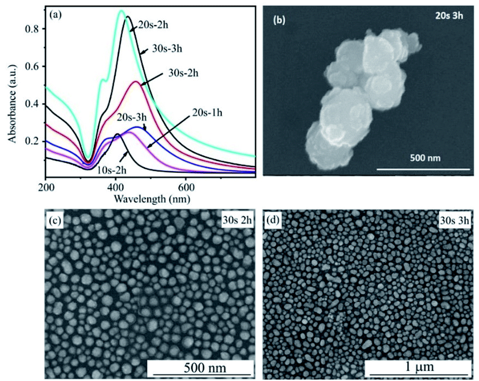 | ||
| Fig. 7 UV-Vis absorbance spectra of AgNPS as a function of deposition time (10 s, 20 s, 30 s) and annealing time (1 h, 2 h, and 3 h) (a) and SEM images of AgNPs for conditions of 20 s–3 h (b), 30 s–2 h (c) and 30 s–3 h (d). | ||
Microstructure properties
The UV-Vis absorption spectra showed that the optimum experimental conditions for the formation of AgNPs having the highest surface plasmon resonance peak are the heat-treatment temperature of 450 °C for 2 h and the silver film thickness of 30 nm. The low magnification SEM images in Fig. 8 show the 3D structure of AgNPs@PSi and the uniform formation of AgNPs on the surface of pyramids. | ||
| Fig. 8 The low magnification SEM images of AgNPs@PSi substrate. | ||
Fig. 9 displays FESEM images of AgNPs@PSi substrates with different pyramid sizes, AgNPs size-distributions and distances between AgNPs. The spherical AgNPs are formed homogeneously and densely on the pyramids. This observation is in good agreement with that obtained by UV-Vis spectra. The size distribution of AgNPs and the distance between AgNPs were fitted with a Gaussian profile. The AgNPs average size and the spacing between particles depend slightly on the size of pyramids. These parameters decrease from 48 nm to 42 nm and from 47 nm to 40 nm, respectively, with an increase of pyramid size because the surface area of the pyramid increases with pyramid size in range of 1 μm and 10 μm. In fact, on the surface of bigger pyramid, the Ag film is thinner at the same deposited condition. As a result, after annealing, the smaller AgNPs are formed corresponding to the higher density of AgNPs and the smaller gap among AgNPs, which is an important factor to decide to the strong LSPR occurrence as observed in the UV-Vis spectra. The smallest average particles size of 42 nm with a gap of 40 nm were obtained for AgNPs@PSi substrates with the pyramid size of 7–10 μm.
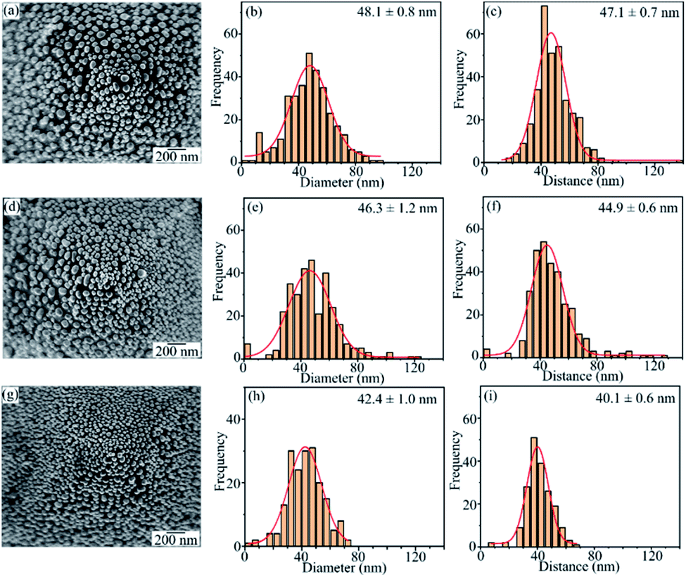 | ||
| Fig. 9 The FESEM images, the size distribution, and the spacing d between grain boundaries of AgNPs@PSi substrates with different pyramid size (a, b, c) 1–3 μm; (d, e, f) 3–7 μm; (g, h, i) 7–10 μm. | ||
Some studies indicated that the electromagnetic field in localized surface plasmon resonance (LSPR) decreases rapidly with the distance from the surface of the metal particle, especially in the range of 10–30 nm.35,36 Moreover, the work of R. Xiu He et al.24 recommended that an increase of particle size from 35 to 65 nm produces stronger LSPR for an excitation of 633 nm. Obviously, our findings meet these conditions and thus, these substrates are suitable to active as SERS surfaces to detect organic molecules.
X-ray diffraction
The X-ray diffraction (XRD) patterns of PSi and AgNPs@PSi substrates recorded by Bruker D8 Advance are shown in Fig. 10. Both patterns show a sharp peak close to 69.1° assigned to the Si (100) reflection. Moreover, the diffractogram of AgNPs@PSi has been compared with the standard powder diffraction card of JCPDS-04-0783 of silver. The appearance of four peaks at 2θ = 38.2, 44.5, 64.8, and 77.4° correspond to (111), (200), (220) and (311) crystal planes of silver crystals. Thus, the XRD study confirms that AgNPs with the face-centered cubic crystal structure are formed on the Si pyramids.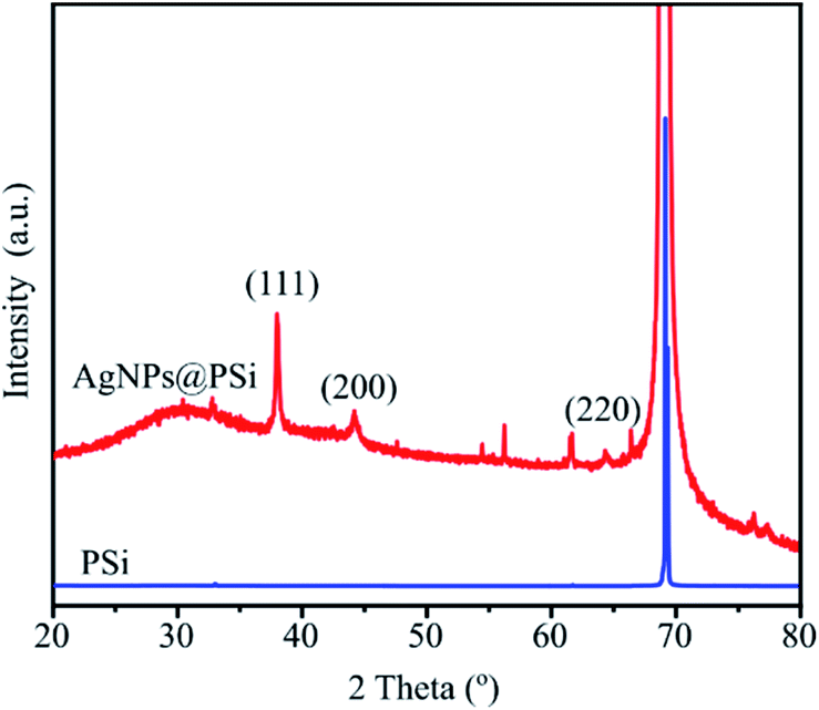 | ||
| Fig. 10 XRD patterns of PSi and PSi@AgNPs substrates. | ||
SERS measurements
To evaluate the effect of pyramid size on enhancement of the signal, Raman spectra with an abamectin concentration of 5.7 × 10⁻⁷ M were recorded. Fig. 11 presents the SERS spectra of substrates with the pyramid sizes of 1–3 μm, 3–7 μm and 7–10 μm. The Raman spectra of substrate without abamectin is also added as reference. All spectra show a characteristic sharp band of silicon at 520 cm−1. The band around 960 cm−1 is due to the vibration of Si–OH on the surface of the Si substrate. In addition, three spectra of SERS substrates with abamectin appear the bands at 624, 860 and 1110 cm−1 attributed to stretching vibrations of C–O and the peaks at 1170, 1274 cm−1 for C–O–C stretching vibrations. The peaks at 1376 and 1447 cm−1 are assigned to C–H bending vibrations of (–CH3) groups. In addition, the band at 1613 cm−1 and 1730 cm−1 correspond to benzene skeleton vibration and C![[double bond, length as m-dash]](https://www.rsc.org/images/entities/char_e001.gif) O of the ester groups of abamectin, respectively.23,37–40 It is noted that the peak intensities of abamectin increase with an increase of Si pyramid size. This finding indicates that the large pyramids lead to a signal enhancement more efficiently than do small pyramids. This result is due to two factors. Firstly, the AgNPs@PSi substrate with large pyramids can trap and scatter excitation light better than can small ones, as revealed in Reflectance spectra section. Moreover, the large pyramids promote a denser formation of AgNPs on pyramids due to their higher surface area, thus enhancing the local electromagnetic field of AgNPs. To achieve a high enhancement factor of the AgNPs@PSi substrate, it is necessary to create large silicon pyramids in range of 7–10 μm. This matter has never been demonstrated in previous works.
O of the ester groups of abamectin, respectively.23,37–40 It is noted that the peak intensities of abamectin increase with an increase of Si pyramid size. This finding indicates that the large pyramids lead to a signal enhancement more efficiently than do small pyramids. This result is due to two factors. Firstly, the AgNPs@PSi substrate with large pyramids can trap and scatter excitation light better than can small ones, as revealed in Reflectance spectra section. Moreover, the large pyramids promote a denser formation of AgNPs on pyramids due to their higher surface area, thus enhancing the local electromagnetic field of AgNPs. To achieve a high enhancement factor of the AgNPs@PSi substrate, it is necessary to create large silicon pyramids in range of 7–10 μm. This matter has never been demonstrated in previous works.
 | ||
| Fig. 11 Raman spectra of abamectin with the concentration of 1 ppm on SERS substrates with different pyramid sizes. | ||
Fig. 12 shows the SERS spectra of abamectin solutions with various concentrations on SERS substrates having a pyramid size of 7–10 μm. The characteristic bands of abamectin at 624, 860, 1022, 1100, 1274, 1376, 1447, 1613 and 1720 cm−1 are detected in all spectra. In particular, the band at 1447 cm−1 is clearly observed even at the low concentration of 5.7 × 10⁻⁹ M. With rising abamectin concentrations, these peak intensities are higher. This observation demonstrates that our SERS substrates possess a good enhancement factor.
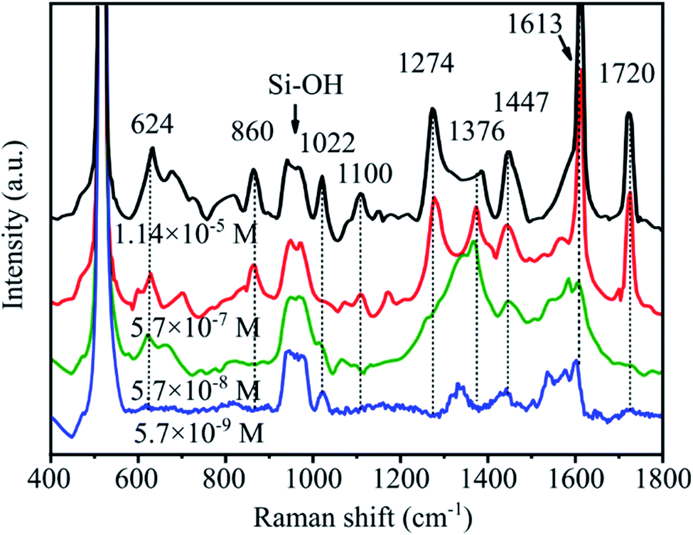 | ||
| Fig. 12 SERS spectra as a function of abamectin concentrations ranging from 5.7 × 10⁻⁹ to 1.14 × 10⁻⁵ M on AgNPs@PSi substrates with pyramid size of 7–10 μm. | ||
To calculate the enhancement factor (EF) value of abamectin, we used the following formula:
| EF = (ISERS/Inormal)/(Nnormal/NSERS) |
The representative peak for abamectin at 1447 cm−1 was also chosen to study the quantitative detection by monitoring the intensity of this band as a function of the abamectin concentration. Fig. 13 shows a good linear fit between the intensities of the 1447 cm−1 band and abamectin concentrations. The fitting equation is
| I = 0.273 × logC + 2.869 |
 | ||
| Fig. 13 The linear relationships of the peak intensity at 1447 cm−1 as a function of abamectin concentrations ranging from 5.7 × 10⁻⁶ to 5.7 × 10⁻⁹ M. | ||
Conclusions
By using anisotropic Si wafers wet-etched in KOH and IPA solutions, and using thermal evaporation and heat treatments of silver thin films, we have successfully fabricated AgNPs@PSi-based SERS substrates. AgNPs with a size range of 42–48 nm are homogeneously and densely formed on the surface of pyramids and the gap between AgNPs is about 40–47 nm. Substrates with these nanoparticle sizes and inter-nanoparticle spacings exhibit the most effective surface plasmonic resonance. In addition, it is found that the pyramid size has significant influence on the enhancement of SERS signal, due to the ability of light-trapping for scattering and their large surface area. The strongest Raman signal was obtained when the base-edge pyramid size was around 7–10 μm. The performance of this SERS substrate including high EF, sensitivity and quantitative ability has been illustrated by the detection of abamectin. Thus, using SERS substrates based on AgNPs of 42 nm and pyramid edges of 7–10 μm, it was possible to detect abamectin molecules at concentrations as low as 5.7 × 10⁻⁹ M, with an enhancement factor of 1 × 10⁶. Such a remarkable SERS substrate promises great potential for practical applications in food security.Author contributions
Nguyen Thuy Ngoc Thuy: synthesize, formal analysis, investigation, writing – original draft, visualization. Huynh Nguyen Thanh Luan: formal analysis, investigation, writing –review & editing. Van Vo Kim Hieu: synthesize, analysis. Mai Thi Thanh Ngan: synthesize, measure. Nguyen Tri Trung: measure, analysis. Le Vu Tuan Hung: review & editing. Tran T. T. Van: conceptualization, investigation, writing – review & editing, supervision.Conflicts of interest
There are no conflicts to declare.Acknowledgements
This research is funded by Ministry of Science and Technology of Vietnam (MOST) under grant number: ĐTĐL.CN-04/19.References
- T. Tišler and N. Kožuh Eržen, Ecotoxicology, 2006, 15, 495–502 CrossRef PubMed.
- S. Kushwaha, I. Anerao, S. Rajput, P. Bhagriya and H. Roy, Cogent Biol., 2020, 6, 1761277 CrossRef.
- R. A. Moreira, G. S. Araujo, A. R. R. Gouveia Silva and M. A. Daam, et al., Ecotoxicology, 2020, 29, 1486–1499 CrossRef CAS PubMed.
- D. K. Lim, D. K. Lim, K. S. Jeon, J. H. Hwang, H. Kim, S. Kwon, Y. D. Suh and J. M. Nam, Nat. Nanotechnol., 2011, 6(7), 452–460 CrossRef CAS PubMed.
- C. Zhang, S. Z. Jiang, C. Yang and C. H. Li, et al., Sci. Rep., 2016, 6, 4–11 CrossRef PubMed.
- P. Zheng, S. K. Cushing, S. Suri and N. Wu, Phys. Chem. Chem. Phys., 2015, 17, 21211–21219 RSC.
- M. Ider, K. Abderrafi, A. Eddahbi, S. Ouaskit and A. Kassiba, J. Cluster Sci., 2017, 28, 1051–1069 CrossRef CAS.
- J. Xu, C. Li, H. Si, X. Zhao and L. Wang, et al., Opt. Express, 2018, 26, 21546–21612 CrossRef CAS PubMed.
- C. Y. Huang and C. H. Chien, Appl. Sci., 2019, 9, 5237 CrossRef CAS.
- A. Roy, A. Maiti, T. K. Chini and B. Satpati, ACS Appl. Mater. Interfaces, 2017, 9, 34405–34415 CrossRef CAS PubMed.
- R. Gao, H. Qian, C. Weng, X. Wang and C. Xie, et al., Sens. Actuators, B, 2020, 321, 128543 CrossRef CAS.
- R. Mei, Y. Wang, Q. Yu, Y. Yin, R. Zhao and L. Chen, ACS Appl. Mater. Interfaces, 2020, 12(2), 2059–2066 CrossRef CAS PubMed.
- J. Li, L. Chen, T. Lou and Y. Wang, ACS Appl. Mater. Interfaces, 2011, 3(10), 3936–3941 CrossRef CAS PubMed.
- G. Yang, X. Fang, Q. Jia, H. Gu and Y. Li, Microchim. Acta, 2020, 187, 310 CrossRef CAS PubMed.
- J. Tang, W. Chen and H. Ju, Sens. Actuators, B, 2019, 287, 576–583 CrossRef CAS.
- C. Zhang, S. Chen, Z. Jiang, Z. Shi, J. Wang and L. Du, ACS Appl. Mater. Interfaces, 2021, 13(24), 29222–29229 CrossRef CAS PubMed.
- C. Wang, K. W. Wong, Q. Wang, Y. Zhou, C. Tang, M. Fan, J. Mei and W. M. Lau, Talanta, 2019, 191, 241–247 CrossRef CAS PubMed.
- S. Li, N. Zhang, N. Zhang, D. Lin, X. Hu and X. Yang, Sens. Actuators, B, 2020, 321, 128519 CrossRef CAS.
- C. Huang, C. Xu, J. Lu, Z. Li and Z. Tian, Appl. Surf. Sci., 2016, 365, 291–295 CrossRef CAS.
- T. Cong, Y. Huang, Y. Zhao, H. Huang and D. Zhang, et al., J. Alloys Compd., 2021, 859, 158389 CrossRef CAS.
- M. K. Nguyen, W. N. Su and B. J. Hwang, Adv. Healthcare Mater., 2017, 6(10), 1–7 Search PubMed.
- S. A. Razek, A. B. Ayoub and M. A. Swillam, Sci. Rep., 2019, 9, 1–8 CAS.
- N. H. Ke, D. A. Tuan, T. T. Thong, N. H. Long, N. H. Thanh and L. V. Tuan Hung, Plasmonics, 2021, 0123456789 Search PubMed.
- R. X. He, R. Liang, P. Peng and Y. Norman Zhou, J. Nanopart. Res., 2017, 19, 267 CrossRef.
- B. Ankamwar, U. K. Sur and P. Das, Anal. Methods, 2016, 8, 2335–2340 RSC.
- Y. Guo, J. Yu, C. Li, Z. Li, J. Pan and A. Liu, et al., Opt. Express, 2018, 26, 21784 CrossRef CAS PubMed.
- T. T. Thuy, M. Sharipov, Y. Lee, B. T. Huy and Y. Lee, Nano Sel., 2020, 1, 499–509 CrossRef.
- M. Haeri and M. Haeri, J. Open Res. Softw., 2015, 3, 2–5 Search PubMed.
- I. Zubel, K. Rola and M. Kramkowska, Sens. Actuators, A, 2011, 171, 436–445 CrossRef CAS.
- E. Abdur-Rahman, I. Alghoraibi and H. Alkurdi, Int. J. Anal. Chem., 2017, 2017, 7542870–7542879 Search PubMed.
- S. Zhong, W. Wang, Y. Zhuang, Z. Huang and W. Shen, Adv. Funct. Mater., 2016, 26, 4768–4777 CrossRef CAS.
- A. Mahmoud Al and B. Lahlouh, J. Appl. Sci., 2017, 17, 374–383 CrossRef.
- G. Yang, Q. Lin, C. Wang and J. Li, J. Nanosci. Nanotechnol., 2012, 12(5), 3766–3774 CrossRef CAS PubMed.
- A. Brioude and M. P. Pileni, J. Phys. Chem. B, 2005, 109(49), 23371–23377 CrossRef CAS PubMed.
- H. Tang, C. Zhu, G. Meng and N. Wu, J. Electrochem. Soc., 2018, 165, B3098–B3118 CrossRef CAS.
- M. Li, S. K. Cushing and N. Wu, Analyst, 2015, 140, 386–406 RSC.
- L. A. F. Dias, E. I. Jussiani and C. R. Appoloni, J. Appl. Spectrosc., 2019, 86, 166–175 CrossRef CAS.
- G. Khattab, W. Abdelghany and M. Abdelmegeed, et al., Arab Univ. J. Agri. Sci., 2019, 82(2), 601–615 Search PubMed.
- Y. Li, Y. Qin, S. Liu and R. Xing, et al., BioMed Res. Int., 2016, 9805675–9805678 Search PubMed.
- W. Guan, L. Tang, Y. Wang and H. Cui, J. Agric. Food Chem., 2018, 66(29), 7568–7576 CrossRef CAS PubMed.
- G. Kumar and R. K. Soni, Plasmonics, 2020, 15, 1577–1589 CrossRef CAS.
- D. Zhang, H. Pu, L. Huang and D. W. Sun, Trends Food Sci. Technol., 2021, 109, 690–701 CrossRef CAS.
| This journal is © The Royal Society of Chemistry 2021 |